Superconducting Strips: A Concept in Thermal Neutron Detection

Dipartimento di Fisica, Università Roma Tor Vergata, and INFN Sezione Roma Tor Vergata, Via della Ricerca Scientifica, I-00133 Roma, Italy
Instruments 2018, 2(1), 4; https://doi.org/10.3390/instruments2010004
Submission received: 29 December 2017
/
Revised: 23 February 2018
/
Accepted: 24 February 2018
/
Published: 2 March 2018
(This article belongs to the Special Issue Advances in Particle Detectors and Electronics for Fast Timing)
Abstract
:In the never-ending quest for better detection efficiency and spatial resolution, various thermal neutron detection schemes have been proposed over the years. Given the presence of some converting layers (typically boron, but 6LiF is also widely used nowadays), the shift towards concepts based on solid state detectors has been steadily increasing and ingenious schemes thereby proposed. However, a trade-off has been always sought for between efficiency and spatial resolution; the problem can be (at least partially) circumvented using more elaborate geometries, but this complicates the sample preparation and detector construction. Thus, viable alternatives must be found. What we proposed (and verified experimentally) is a detection scheme based on the superconducting to normal transition. More precisely, using a boron converting layer, the α particles (generated in the (n, α) reaction) crossing a low critical temperature superconducting strip some 10 µm wide have been detected; the process, bolometric in nature and based on the ionization energy loss, is intrinsically fast and the spatial resolution very appealing. In this work, some of the work done so far will be illustrated, together with the principles of the measurement and various related problems. The realization of the detector is based on industrial deposition and photolitographic techniques well within the grasp of a condensed matter laboratory, so that there is substantial room for improvement over our elementary strip geometry. Some of the plans for future work will also be presented, together with some improvements both in the choice of the materials and the geometry of the detector.
1. Introduction
The use of neutron detectors dates back from the early days of nuclear physics [1]. Besides their use in fundamental studies, the rapid development of suitable devices also took place in connection with nuclear fission phenomena where the importance of thermal neutrons became readily apparent. Since then, a variety of different techniques have been developed, with different physical phenomena exploited in relation to the energy range of interest. Thus, the recoil or scattering phenomena in the detecting material are used in the meV neutron energy range while the absorption phenomena are preferred in the thermal energy (that is, typically 25 meV) range. This is due to the very high value of the absorption cross section which, in some cases, can easily exceed 103 barn. In either case, neutron detection is achieved by means of the ionization energy loss suffered by the secondary charged products of the reaction which, in the simplest cases, takes place in a gas chamber with an appropriate electrode configuration. Typical examples of gas chambers are 3He and BF3 tubes for thermal neutrons and fission counters for both thermal and fast neutrons.
The situation evolved significantly with the advent of the semiconductor industry, when Ge and Si became routinely available and the first charged particle detectors realized. It is at that time that the concept of an absorbing/converting layer (typically boron or 6LiF) coupled to a semiconductor detector started evolving as a strong candidate for thermal neutron detection and spectrometry [2]; see [3] for a more recent detailed contribution. It must be noted, though, that fast neutrons (for instance, those emitted in D-D and D-T reactions from a hot fusion plasma), can also be detected by a Si detector, albeit with a different physical mechanism. However, it must be pointed out that when very high efficiencies (and moderate spatial resolutions) are required, 3He high pressure tubes are still the first choice. As a matter of fact, these instruments are still the workhorse in a range of diverse applications, for instance, as time of flight detectors in experimental stations located at spallation or reactor neutron sources. Recently an interesting scheme capable of detecting both thermal and fast neutrons has also been proposed based on the use of Chemical Vapour Deposition (CVD)-grown diamond single-crystals coated with 6LiF [4]. For a more extensive and up to date review on the current state of development on solid-state neutron detectors see the reviews [5,6].
However, there are applications—such as in nuclear medicine, some diffraction techniques, and beam profile studies—where a sub-millimeter spatial resolution is required for best results. In this case, it is clear that special solutions must be sought for using some techniques borrowed from condensed matter research, such as UV deposition and lithography. Also, we must bear in mind that high spatial resolution means working with small enough sensing surfaces which, in turn, affects the overall efficiency. Thus, the intended devices must have a much more elaborate spatial geometry or structure. Some progress has been made in thermal neutron high resolution imaging using micro channel plates or MCPs where the glass surfaces have been enriched in boron [7], reaching efficiencies in the order of 20% and resolutions of 30 µm, though radiation hardness may be a serious problem. Better spatial resolution can also be achieved but at the cost of reducing the efficiency at the percent level, thus making alternative approaches more attractive.
Along these lines, and relying on the excellent work done over the years by several authors on the detection of ionising radiation by means of superconductors (for a review see [8,9,10]), we put this experience to our advantage by merging two apparently distant fields; more specifically, a prototype configuration has been realized with a superconducting strip particle detector (SSPD) coupled to a boron converting layer (a bilayer structure), and its behaviour as a neutron counter successfully demonstrated by measuring some of its properties.
This short review is structured as follows. First comes an overview of the work done over the years on superconducting (sc) detectors for ionising radiation, with an emphasis on the detection of α-particles and related physical problems. The operating principle of the detector will then be explained, with some attention devoted to work done by our group, describing and summarizing all important aspects of sample preparation, characterization, and measurement of detector properties. The original results of this work have been reported in two separate papers [11,12], which will furthermore be referred to as P1 and P2, respectively. There, we assessed and verified the proposed detection principle by irradiation with a pulsed neutron beam at the INES beamline of the ISIS spallation source (STFC-RAL, Didcot, UK). Samples made of different materials, namely Nb and NbN, and sizes were measured so that an appropriate comparison could be made.
Finally, future developments and work in progress will be discussed.
2. Basic Operating Principle and Related Physics
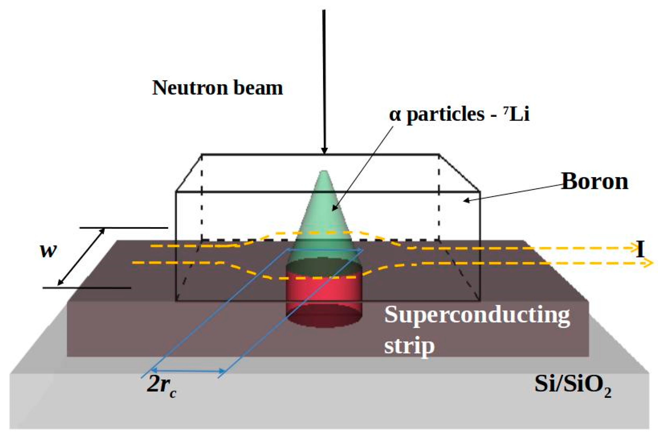
Detection of a charged particle in a SSPD kept below its critical temperature (Tc) relies on the ionization loss suffered while crossing the material. Assuming normal incidence, creation of a “hot” normal-state cylindrical region takes place with the axis as the particle trajectory (see Figure 1 for details).
According to a bolometric model and assuming cylindrical symmetry, one can write an energy balance between the energy lost and the enthalpy per unit volume of the material [13] thus,
where rc defines the radius of the circular cross section normal to the charged particle trajectory and h is the enthalpy per unit volume. This means that Δh is the enthalpy difference per unit volume for the superconducting to normal transition which, in turn, can be written in terms of the thermodynamic critical magnetic field of the material: Δh = B2c(T)/2µ0, with Bc(T) → 0 as T → Tc. Thus, close to Tc switching to the normal state is easier (on energetic grounds). Since hot-spot measurements are performed at a fixed temperature, so is the value of rc. Experimental evidence of the superconducting to normal transition is obtained through measurement of a finite voltage drop across the strip.
Δh πr2c = (dE/dx)ion
As a matter of fact, α particle detection by means of superconducting strips started as early as 1949 with the seminal work by Andrews et al. [14]. These authors measured pulses coming from a long NbN (actually CbN) strip kept at low temperature and irradiated by α-particles coming from a polonium source. Other authors subsequently observed the same phenomena and attempted a first quantitative analysis [15], but a more thorough understanding of the problem came with more recent work [16,17]. It has been found that the process, a bolometric one, can be modelled using a classical heat transport equation, yielding results in good agreement with the experimental data. In particular, assuming the lattice contribution to heat transport is negligible, the deduced radius of the hot normal region is almost the same previously found (Equation (1)) by means of a much simpler argument. Moreover, under the above assumption (no lattice contribution), good agreement with data implies that relaxation times are very fast (in the order of 1 ns or less). This is somewhat confirmed by the observation of the time structure of the measured voltage pulses [17]. The size of the hot region is closely connected to the amplitude of the observed voltage pulse. Assuming a uniform material with critical current Ic(T), it is reasonable to write the following relation for the critical current under irradiation Iα [17]
where explicit temperature dependence has been indicated, w is the film width, and 2rc the diameter of the circular cross section of the hot spot. The physical meaning of this relationship is easily appreciated: the presence of the normal (resistive) region causes a shrinking of the current channel, so that at a fixed bias current (Ib) the critical current density (Jc) can be locally exceeded. This, thus, causes a transition along the entire width of the strip. It must be noted that “partial” transitions not involving the entire width of the strip may also take place, i.e., the so called self-recovering pulses. Since the voltage drop occurs only across the normal zone, it follows that the maximum value of the voltage amplitude is given by
with ρ the normal state residual resistivity of the material and where Jc is the local transport critical current density. Using reasonable estimates for typical material parameters of elemental superconductors, one obtains minimum values for rc and V in the order of 1 µm and 10 mV, respectively. More appropriate figures will be given later, when discussing the results of real experiments. Also, typical values of the ionization energy loss for particles in Nb and NbN thin films are in the order of 200 keV (200–600 keV/µm, depending on the incident α particle energy) and projected ranges around 2 µm (at least for particles hitting the strip at angles reasonably close to normal incidence). For future reference, it must be noted that when 7Li ions are involved, these figures are about 60% of those appropriate to α particles [18]. In both cases, since the SSPD is deposited on a substrate, this means that the charged particle will deposit most of its energy in it. Thus, heating of the substrate can, in principle, interfere with measurement since heat can flow back to the superconductor via phonon transport. This problem has been tackled in [18] where it was shown that a proper thermal decoupling is mandatory in order to ensure reliable operation of the detector. A proper understanding of all details of the heat pulse propagation (related to pulse rise-time) is beyond the scope of the present work, but essentially the behaviour of these transient phenomena is explained in terms of equilibrium or non-equilibrium models depending on the relative coupling between electron and phonon populations of the superconducting material [19,20]. An interesting and extensive discussion of the two approaches related to the operation of superconducting strip particle detectors can be found in [21], where the situation is described in some detail and estimates are made of the various time scales involved. For quite recent work on this subject, see also [22]. These authors provide an extensive, up-to-date review more oriented towards photon detection and also discuss, in detail, the realization of multiple devices for single-photon counting.
Iα (T) = Ic(T)(1 − 2rc/w)
V = 2rcρJc
If we now think of adding a layer of boron on top of the SSPD, we are led to the working principle of the neutron detector (Figure 1). Just observe that thermal neutron detection takes place thanks to absorption according to the reactions 10B + n → + 7Li (BR 7%, with E = 1.47 meV and ELi = 0.84 meV) and 10B + n → + 7Li + (478 keV) (BR 93%, with E = 1.71 meV and ELi = 1.02 meV) where the relative branching ratios are given. Since the incident neutron energy is in the thermal region, the charged secondary products are emitted almost at 180° so that either particle is detected by the underlying SSPD, thereby increasing the efficiency. It can be shown that for the typical conditions of the experiments performed so far (superconducting films with thickness in the order of 0.3–0.5 µm), the absorption probability is in the order of 10−4. Furthermore, at the INES beamline (Rutherford Appleton Laboratory) used in the experiments, the gamma flux is an order of magnitude lower compared to neutrons so that the overall effect of gamma radiation can be safely ignored even at count rates less than 1 c/s typical of this experimental setup.
Using this bilayer configuration (B + SSPD), strips were prepared of various dimensions and two different superconductors, namely N and NbN. We then added boron layers, both natural and 10B only. At first, experiments were performed with Nb + B to demonstrate the principle of the measurement. Then, NbN + B samples were also irradiated with the added advantage of working at slightly higher temperatures and much higher detected voltages with no need for any pre-amplification stages.
For the sake of precision, it should be noted that some work similar to ours has been done by Ishida and co-workers in a series of papers. Initially, a scheme based on the absorption in the superconducting compound MgB2 has been proposed [23] (so that the same material acts both as a converting and detecting medium) where voltage pulses under irradiation have been observed. In later works [24,25] an interesting concept has been proposed where detection is made possible by a boron layer superimposed on a Nb nanowire. Also, in this case, the time structure of the voltage pulses has been investigated under neutron irradiation. However, elaborate as these schemes may be, it must be pointed out that in these works no estimate on the efficiency is provided, nor a study of the count rate has been attempted. Thus, it is difficult to assess their relevance toward the realization of a practical detector.
We turn now to the description of recent experiments and summarize their results. Emphasis will be given to the relevant aspects, with all details being available in P1 and P2.
3. Sample Preparation and Characterization
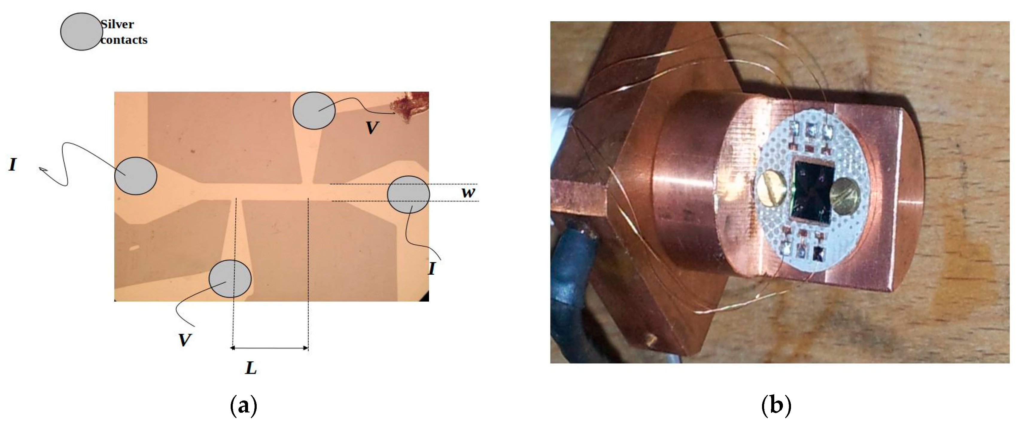
Two distinct experiments were run with different superconducting materials, namely Nb and NbN. Both of them exhibit excellent mechanical properties and radiation hardness, allowing use at intense neutron sources with no significant degradation in their superconducting properties. In particular, NbN can tolerate a fast neutron dose of 1019 n/cm2 with a decrease in the order of only 1% in the critical temperature [13]. Nb and NbN thin films were deposited on Si substrates according to procedures outlined in P1 and P2, briefly summarized here. The Si substrates are fabricated with 1 µm of SiO2 thermally grown oxide on top, and Nb or NbN films are prepared by magnetron sputtering at an Ar gas pressure in the range of 10−3 mbar. The final thickness of the samples was measured ex situ by a profilometer, also used to calibrate the Nb sputtering rates. Before the deposition, the substrates were covered with photoresist and processed using a standard photolithographic technique in order to define the strip geometry. The latter consists of a rectangular strip with four terminal pads for the electrical connections, as shown in Figure 2.
After the deposition, the final structures were obtained by lift-off. Strip detectors with length L in the range 400–800 µm, width w = 10–20 µm, and thickness d = 150–200 nm were obtained. The neutron sensitive boron layer was deposited on all the strip detectors by electron beam evaporation through a circular mechanical shadow mask, for a thickness of 450 nm. Because of the 20% abundance of 10B in natural B, this thickness gives a calculated efficiency of roughly 1% for the (n-α) reaction occurring in the thermal energy range. Depositions of isotopic 10B were also performed for a thickness of 90 nm which, in terms of absorption, is equivalent to the previous samples. After preparation and prior to neutron irradiation, the samples were characterized by means of electrical measurements (both in our laboratory and mounted in position at the pulsed neutron source). Data was taken just before irradiation using a standard four contact geometry, biasing the samples with a current Ib and measuring the voltage V using a Keithley 2400 Source Meter. The noise figure on Ib is ΔIb = 50 µA and 1 µA for Ib in the ranges of 10 mA and 100 mA, respectively. The samples were fixed at the tip end of a cold finger inside a He-flow cryostat which allowed for measurements in the temperature range 1.8–20 K with an accuracy of ΔT = 0.01 K, as measured by a thermometer located in contact with the sample holder close to the sample.
Preliminary measurements were performed to characterize the detectors and to determine some useful parameters for their calibration. In Figure 3, the resistance (R), normalized with respect to its value in the normal state (RN), is shown as a function of the temperature T for Nb and NbN strips not exposed to the neutron beam. All samples were of comparable quality, showing small dispersion in their electrical characteristics. The zero resistance critical temperature (Tc0) here reported is 8.46 and 13.67 K for Nb and NbN strips of thickness d, respectively.
The current density J = I/(W × d) versus V characteristics have been measured at the same reduced temperature t = T/Tc0 = 0.89 K for the same strips reported in Figure 3. The current density increases up to the critical value Jc where a sudden increase in the voltage is measured. From the data, a higher Jc for Nb than for NbN can be inferred, as well as a correspondent voltage step about one order of magnitude larger in the case of NbN with respect to Nb. For J > Jc, the J-V characteristics are Ohmic, as expected. From the slope of these characteristics and the strip size, the resistivity values in the normal state (just above the resistive transition) turned out to be N = 2.5 µΩcm and 250 µΩcm for Nb and NbN, respectively. The much higher value of ρ for NbN is responsible for the higher switching voltage measured. This is in agreement with Equation (3), but Jc and rc dependency should be also taken into account.
4. Data Collection and Summary of Results
Data was always taken with the strips at a fixed temperature, reasonably close to Tc. Since Ic is a decreasing function of temperature, the bias current (to be set at a value just below Ic in order to make the transition more energetically convenient) is low enough to avoid self-heating effects in the contacts (see Figure 4 for details).
However, there are two distinct sets of measurements that can be performed to assess the properties of the detector. On the one hand, there are purely “electrical” measurements, that is I-V curves with irradiation on/off. Since the value of the critical current drops during irradiation (see Equation (2)), this effect must be clearly visible in the data. As a matter of fact, it is the signature of neutron detection. On the other hand, there is the “classical” measurement of the count rate. Once this is done, the count rate as a function of bias current has been studied, finding linear behaviour in agreement with previous measurements on strips directly irradiated by α particles [18]. However, there are a few points to be examined before discussing the data:
- Effect of contacts: in one set of measurements, electrical contact with the measurement apparatus was made by means of silver paint droplets on the contact pads. In principle, this can be a problem since Ag may become activated under thermal neutron irradiation with subsequent decay via charged products. To circumvent the problem, samples used in subsequent measurements were used where electrical contact was made via micro-bonding. Upon irradiation, no difference has been observed with previous measurements in the same experimental conditions, so the effect is deemed to be negligible and the bonding technique immaterial.
- Phonon decoupling: this has been most simply accomplished with the use of SiO2 on top of the substrates. This amorphous layer which is 1 µm thick seriously hinders phonon propagation from the crystalline Si back to the superconducting (sc) strip. It can be estimated that the phonon mean free path in the oxide is probably around 100 nm, although the value at low temperatures is strongly dependent on the film deposition technique. It should also be noted that boundary scattering from the interfaces could play a role in limiting the amount of heat transferred back to the sc strip. Crittenden [17] demonstrated that phonon decoupling takes place with just 30 nm of varnish deposited on the substrate.
- Blank measurements: in order to confirm the validity of our first set of measurements, data was also taken from irradiating a “naked” strip that is just Nb with no boron layer superimposed. Following the same procedure, no counts were recorded for times up to 30 min after starting the irradiation, thereby confirming that the boron layer is indeed responsible for neutron absorption and indirect detection.
- With the experimental conditions described in P1 and P2 the expected count rate is in the order of 9 counts/min. This rate, which is quite low considering also the limited time available for irradiation, did not allow the performance any systematic study of the pulse shape and was barely sufficient to accumulate the statistics needed to demonstrate detector operation.
All measurements under neutron irradiation have been taken opening a system of mechanical jaws, so the two experimental conditions are labelled as jaws open or closed, respectively. The neutron beam at the INES beam line has energies in the thermal and epithermal regions, with a peak at En = 25 meV and with an estimated fluence at the sample position of 2 × 10⁵ n/s/cm2.
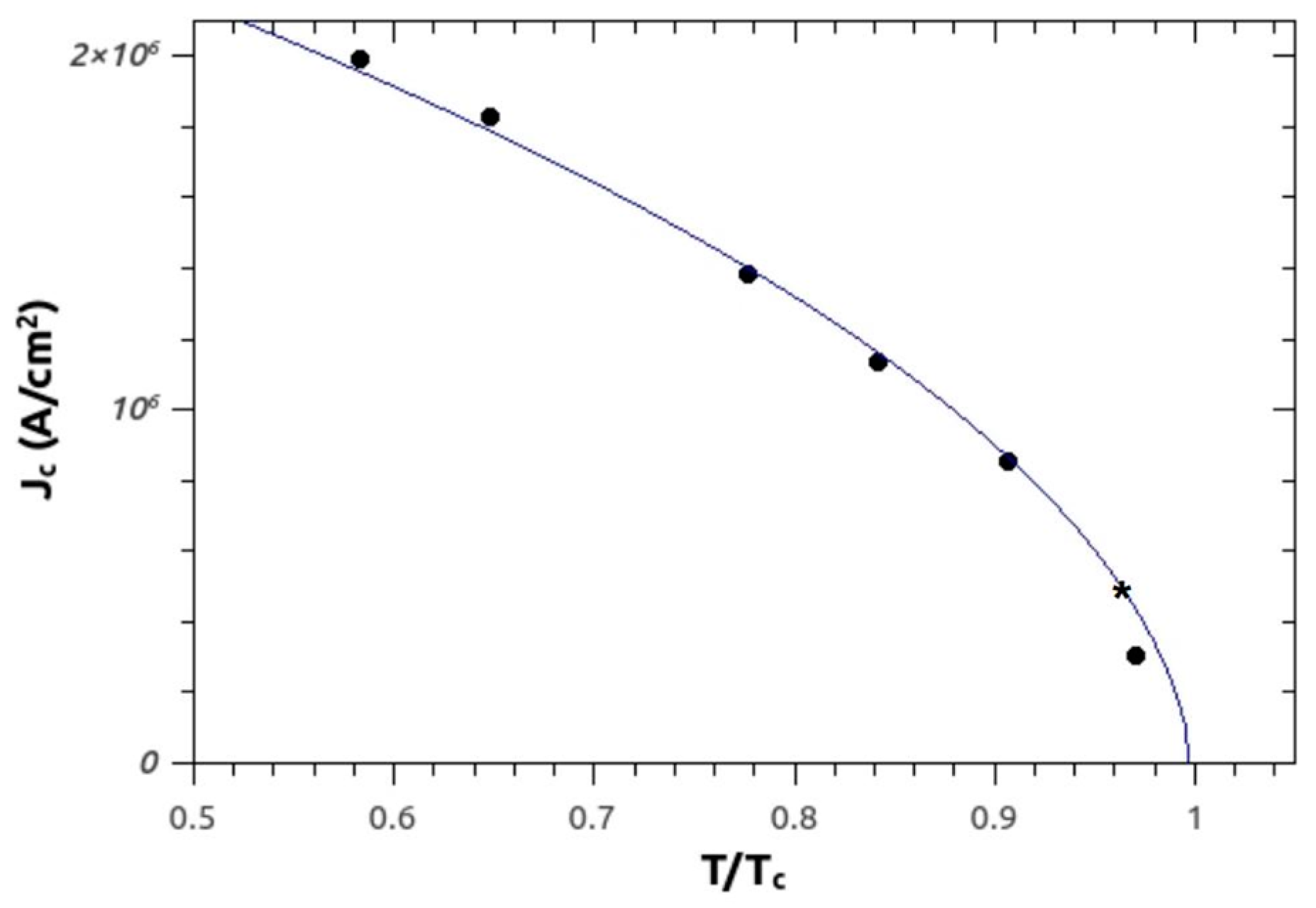
Critical current data was taken (at a fixed temperature T) opening the jaws, then slowly increasing the bias current until a transition was observed. The switching point defined the critical current under irradiation. In Figure 5, the magnitude of the critical current jump in presence of irradiation is shown. The data shown refer to one of the NbN samples examined in P2 and a decrease in the order of 25% in the critical current is easily appreciated. Also to be noticed is the magnitude of the voltage at the switching point, in excess of 10 V. As previously stated, this value, directly measured at the sample with no preamplification at all, is related to the high normal state resistivity of NbN immediately above the transition.
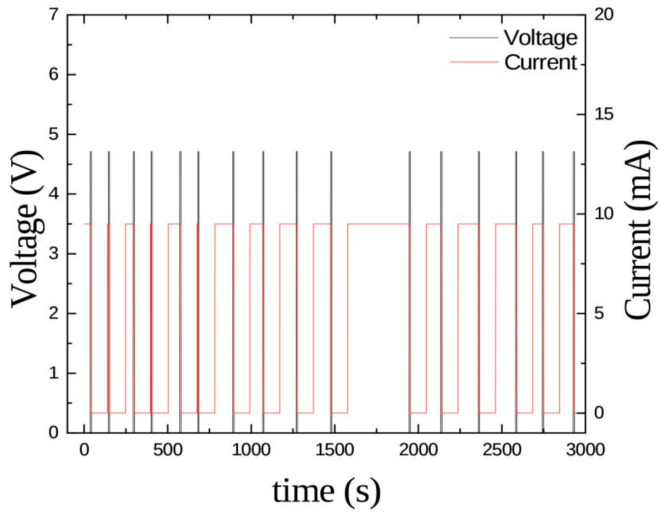
For the same reason, the switching values for Nb strips measured in comparable conditions do not usually exceed 40–50 mV (see P1). There also other reasons to suggest NbN as a stronger candidate for this kind of detector: higher Tc and lower Jc allow operation at higher temperatures and reduced bias currents, reducing the importance of electrical and thermal fluctuations. Moreover, as noted in P2, flux-flow effects related to vortex dynamics allow for better definition of the bias current close to transition. Inverting the simple model relation (2) we can infer a diameter of the hot-spot in the order of 5 µm, which is the right order of magnitude. Moreover, since Δh for Nb and NbN (for Nb, see for instance [23]) is not very different (at the same temperature), we see from (1) that we may take this value as typical. On the other hand, measurement of the count rate is performed with both temperature and bias current fixed. However, since the strip is not self-resetting a proper dead time must be chosen to allow for recovery. In other words, once the strip has undergone a superconducting to normal transition it has to be brought back to the superconducting state (in the “ready” state). This is accomplished by switching off the bias current and waiting long enough for the sample to regain a temperature T < Tc. With a trial and error procedure monitoring the temperature value after the transition, a safe value of 120 s was chosen to wait before ramping up the bias current again. By definition, this is just the dead time τ of the detector. This unusually large value has been dictated primarily by the use of a He flow cryostat (as opposed to a liquid He bath where cooling is much faster). As already noted, the expected count-rate is in the order of 0.1 c/s so that the classical model of a non-paralyzable counter can still be used to extract the true count rate, where Ctrue = Cexp/(1 − τ Cexp). Despite the fact that τCexp ~ 0.3–0.7 for the data shown in Figure 3 of P1, inverting the above relation one can verify that Ctrue can still be estimated with good sensitivity. A typical stretch of data is shown in Figure 6 where V-t and I-t traces are plotted together. Voltage spikes correspond to a detection event, followed by a drop to zero of the bias current for a time duration. The detector is then ready again.
It is interesting to note that the correction formula is normally applied in connection with high count rates and relatively short dead times, while the present case represents a situation of long dead times and low count rates.
Thus, there is a distribution of waiting times (when the bias current is on, until a voltage spike appears) that, in principle, could be measured. This was not possible due to limited statistics, but a rough analysis showed that out of a total of N intervals, the number of these with a duration shorter than the average is larger than N/2 as predicted by a Poisson distribution.
Remaining at fixed temperature T, the same procedure can be repeated by slowly increasing the bias current and measuring the true count rate again. Thus, we were able to graph the count rate as a function of the bias current (see Figure 6 of P1), obtaining a linear behaviour. This is in agreement with results found in [17] where the count rate has been measured for a wider range of currents. The observed count rate has been then compared to the predicted value obtained using beam-line data, such as neutron fluence and energy distribution. Assuming that the absorbed beam fraction by a film with thickness t is nBσabst in the thin-target limit and that an α or a 7Li ion is always detected, the measured value is a factor of 3 smaller than the prediction. Apart from absolute flux data, there are several sources of uncertainty: the highest value of the count rate we were able to estimate (the one we compared with prediction) is almost certainly not the highest and the film boron density used in the absorption calculation is certainly lower than the bulk figure used here, possibly by as much as 10%. Also, in view of the strip geometry used, the escape probability Pα(E) must be correctly estimated since charged particles emitted at large angles may easily escape detection. Given the relatively high Q-values of the reactions involved, the escape probability can be taken as energy-independent and estimated using calculations presented in [26] where a similar geometry has been considered in some detail. Thus, a value Pα ~ 0.5 has been chosen.
Using similar arguments the detection efficiency can also be estimated. This turned out to be 0.5% at the thermal peak (En = 25 meV). Without resorting to complicated geometries, this figure can be easily improved up to 2%, just increasing the thickness of the boron absorber. Together with a spatial resolution of 10 µm, this makes this configuration already attractive. However, it is a generally accepted view [26] that the thickness of the absorber should not exceed 2 µm, seeking a compromise between detection probability and escape probability. Above this limit value, the escape probability starts decreasing so that the overall detector performance is negatively affected. It is clear then that we must think of more elaborate geometries, both planar and 3D.
5. Conclusions and Overview
Although in P1 and P2 it has been demonstrated that the operating principle of the detector is sound, more work has to be done to understand its properties thoroughly. The relatively high values of the switching voltages (around 10 V for NbN) and the linear behaviour of the count rate as a function of the bias current are encouraging, but a wider current range should be explored, and the time structure of the voltage pulses should be properly investigated. Also, a systematic study of the effect of the strip width should be carried out to optimize the count rate. However, with estimated values of rc in the order of a few microns, widths of 10–20 µm are likely to be appropriate. Pursuing these objectives with present day sources is not an easy task due to the quite low count rate available. Another obvious improvement over the present setup would be using a liquid He cryostat (with some beam loss due to neutron scattering in helium). Improved heat exchange would allow us to choose a much shorter dead time τ (the recovery time of the strip), possibly in the order of 1–5 s so that, in principle, higher flux rates could be managed. This figure is more than adequate noting that in state-of-the art neutron sources (pulsed and reactors) fluxes in the range 106 n/s/cm2 are available in the thermal and epithermal range, with predicted maximum count rates in the order of 1 c/s at the strip position. Also, there is significant room for improvement towards a better spatial resolution: the strip width can be reduced down to 1 µm using optical techniques based on lithography, though at the expense of a loss of efficiency, since this is proportional to the strip area. In principle, strips of sub-micrometer width can also be prepared, but only using electron beam lithography or complex optical instrumentation. However, a real improvement could only be achieved with more complicated geometries such as multifingers (several parallel strips) and crossed lines (possibly superimposed). Using information from neighbouring strips, the spatial resolution could be lowered down to 5 µm without reducing the strip width (and efficiency). Polarization and readout are not a problem, since all contacts to/from the strip can be directed to wide bonding pads where contact with the equipment is made using standard automatic bonding techniques borrowed from the semiconductor industry. For prototype building, the possibility of using 6LiF as an absorber has also to be taken into account. The lower value of the absorption cross section (compared to 10B) is compensated by a much easier deposition procedure of layers with thickness in the range of 1–2 µm.
The use of High-Tc superconducting materials can also be considered, but the simple crystalline structure of many low-Tc superconductors makes them more attractive when ease of deposition and patterning is considered. Also, the higher critical fields in high-Tc compounds imply a higher Δh and a lower rc with a decrease in sensitivity. Moreover, working at low temperatures is no longer a problem nowadays. With modern cryocooler systems (or pulsed tubes), temperatures down to 1 K can be easily attained so that one can safely choose a working region around 10 K. Therefore, it is likely that, at the present stage of development, following the low Tc route will lead to an easier implementation and better prototype study.
Acknowledgments
It is a pleasure to thank all the people who participated in the research whose results I reported in this work. Special thanks are due to M.Cirillo and P.Belli for a critical reading of the manuscript.
Conflicts of Interest
The author declares no conflict of interest.
References
- Amaldi, E.; Fermi, E. On the absorption and diffusion of slow neutrons. Phys. Rev. 1936, 50, 899–928. [Google Scholar] [CrossRef]
- Rose, A. Sputtered Boron Films on Silicon Surface Barrier Detectors. Nucl. Instr. Methods 1967, 52, 166–170. [Google Scholar] [CrossRef]
- Almaviva, S.; Marinelli, M.; Milani, E.; Prestopino, G.; Tucciarone, A.; Verona, C.; Verona-Rinati, G.; Angelone, M.; Lattanzi, D.; Pillon, M.; et al. Thermal and fast neutron detection in chemical vapor deposition single-crystal diamond detectors. J. Appl. Phys. 2008, 103, 054501. [Google Scholar] [CrossRef] [Green Version]
- Petrillo, C.; Sacchetti, F.; Toker, O.; Rhodes, N.J. Solid State Neutron Detectors. Nucl. Instr. Methods 1996, 378, 541–551. [Google Scholar] [CrossRef]
- Caruso, A.N. The physics of solid state neutron detector materials and geometry. J. Phys. Condens. Matter 2010, 22, 443201. [Google Scholar] [CrossRef] [PubMed]
- McGregor, D.S.; Hammig, M.D.; Yang, Y.-H.; Gersch, H.K.; Klann, R.T. Design considerations for thin film coated semiconductor thermal neutron detectors. Nucl. Instr. Methods 2003, 500, 272–308. [Google Scholar] [CrossRef]
- Siegmund, O.H.W.; Vallerga, J.V.; Tremsin, A.V.; Feller, W.B. High Spatial and Temporal Resolution Neutron Imaging with Microchannel Plate Detectors. IEEE Trans. Nucl. Sci. 2009, 56, 1203–1209. [Google Scholar] [CrossRef]
- Gray, K.E. Non-equilibrium Superconductivity for Particle Detectors. In Proceedings of the International Workshop on Superconductive Particle Detectors, Torino, Italy, 26 October 1987; p. 1. [Google Scholar]
- Barone, A. Why Superconductive detectors? Nucl. Phys. B 1995, 44, 645–666. [Google Scholar] [CrossRef]
- Boot, N.E.; Goldie, D.J. Superconducting particle detectors. Supercond. Sci. Technol. 1996, 9, 493–516. [Google Scholar] [CrossRef]
- Merlo, V.; Salvato, M.; Cirillo, M.; Lucci, M.; Ottaviani, I.; Scherillo, A.; Celentano, G.; Pietropaolo, A. Hybrid superconducting neutron detectors. Appl. Phys. Lett. 2015, 106, 113502. [Google Scholar] [CrossRef]
- Merlo, V.; Salvato, M.; Lucci, M.; Ottaviani, I.; Cirillo, M.; Scherillo, A.; Schooneveld, E.M.; Vannozzi, A.; Celentano, G.; Pietropaolo, A. Meta-Material for nuclear particle detection. J. Phys. D Appl. Phys. 2017, 50, 045601. [Google Scholar] [CrossRef]
- Wagner, R.G.; Gray, K.E. Superconducting Thin Film Vertex Detector for SSC Applications. In Proceedings of the International Workshop on Superconductive Particle Detectors, Torino, Italy, 26 October 1987; p. 204. [Google Scholar]
- Andrews, D.H.; Fowler, R.D.; Williams, M.C. The Effect of Alpha-particles on a Superconductor. Phys. Rev. 1949, 76, 154. [Google Scholar] [CrossRef]
- Sherman, N.K. Superconducting Nuclear Particle Detector. Phys. Rev. Lett. 1962, 8, 438. [Google Scholar] [CrossRef]
- Spiel, D.E.; Boom, R.W.; Crittenden, E.C. Thermal Spikes in Superconducting Thin Films of Sn and In. Appl. Phys. Lett. 1965, 7, 292–294. [Google Scholar] [CrossRef]
- Crittenden, E.C.; Spiel, D.E. Superconducting Thin-Film Detector of Nuclear Particles. J. Appl. Phys. 1971, 42, 3182–3188. [Google Scholar] [CrossRef]
- Ziegler, J.F. Helium Stopping Power and Ranges in All Elements; Pergamon Press: New York, NY, USA, 1977. [Google Scholar]
- Skocpol, W.J.; Beasley, M.R.; Thinkam, M. Self-heating hotspots in superconducting thin-film microbridges. J. Appl. Phys. 1974, 45, 4054–4066. [Google Scholar] [CrossRef]
- Gray, K.E.; Kampwirth, R.T.; Zasadzinsky, J.F.; Ducharme, S.P. Thermal propagation and stability in superconducting films. J. Phys. F Met. Phys. 1983, 13, 405. [Google Scholar] [CrossRef]
- Wedenig, R.; Niinikoski, T.O.; Berglund, P.; Kyynäräinen, J.; Costa, L.; Valtonen, M.; Linna, R.; Salmi, J.; Seppä, H.; Suni, I. Superconducting NbN microstrip detectors. Nucl. Instr. Meth. 1999, 433, 646–663. [Google Scholar] [CrossRef]
- Cristiano, R.; Ejrnaes, M.; Casaburi, A.; Zen, N.; Ohkubo, N. Superconducting nano-strip particle detectors. Supercond. Sci. Technol. 2015, 28, 12404. [Google Scholar] [CrossRef]
- Ishida, T.; Nishikawa, M.; Fujita, Y.; Okayasu, S.; Katagiri, M.; Satoh, K.; Machida, M. Superconducting MgB2 thin film detector for neutrons. J. Low Temp. Phys. 2008, 151, 1074–1079. [Google Scholar] [CrossRef]
- Ishida, T.; Yoshioka, N.; Narukami, Y.; Shishido, H.; Miyajima, S.; Fujimaki, A.; Hidaka, M. Toward mega-pixel neutron imager using current-biased kinetic inductance detectors of Nb nanowires with 10B converter. J. Low Temp. Phys. 2014, 176, 216–221. [Google Scholar] [CrossRef]
- Ishida, T.; Miyajima, S.; Narukami, Y.; Yoshioka, N.; Shishido, H.; Hidaka, M.; Fujimaki, A. Toward neutron radiography using two arrays of Nb-based current-biased kinetic inductance detectors with 10B converter sandwiched in-between. IEEE Trans. Appl. Supercond. 2015, 25, 2401304. [Google Scholar] [CrossRef]
- Hoglund, C.; Birch, J.; Andersen, K.; Bigault, T.; Buffet, J.C.; Correa, J.; Khaplanov, A. B4C thin films for neutron detection. J. Appl. Phys. 2012, 111, 104908. [Google Scholar] [CrossRef]
Figure 1.
Pictorial view of the hot spot creation in the sc strip. For later convenience, the incoming neutron beam generating α-particles in the B film is also shown. Note, the bias current lines being pushed out of the normal zone to the sides of the strip. To simplify matters, the α-particle is supposed to be emitted in a direction normal to the strip (Adapted from [11], with the permission of AIP Publishing).

Figure 2.
Picture of the real strip (a) with contact pads for current bias and voltage readout. The strip width is W = 10 µm. In (b) the strip mounted on the cold finger with all leads in place. (a) is reproduced from [11], with the permission of AIP Publishing).
Figure 2.
Picture of the real strip (a) with contact pads for current bias and voltage readout. The strip width is W = 10 µm. In (b) the strip mounted on the cold finger with all leads in place. (a) is reproduced from [11], with the permission of AIP Publishing).

Figure 3.
Normalized resistance of two Nb and NbN strips, showing the onset of the superconducting state at Tc (Adapted from [12], with the permission of IOP Publishing).
Figure 3.
Normalized resistance of two Nb and NbN strips, showing the onset of the superconducting state at Tc (Adapted from [12], with the permission of IOP Publishing).
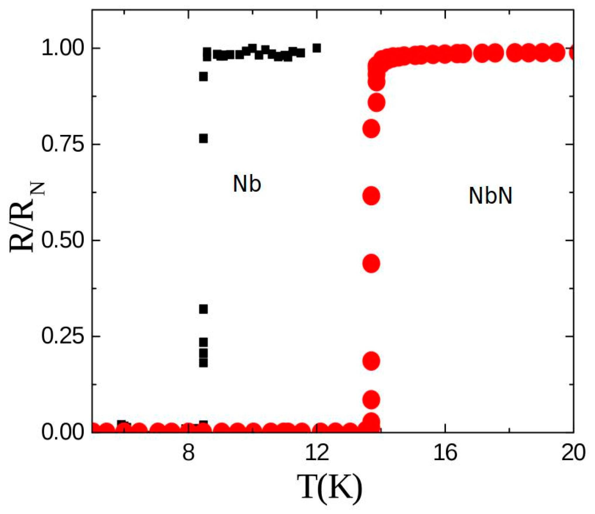
Figure 4.
Critical current curve as a function of reduced temperature t for the Nb strip. Also shown (marked by a *) is one of the possible operating points close to Tc, which may be chosen for the measurements. The continuous line is a fit using a (1 − t2)3/2 dependence (Adapted from [12], with the permission of IOP Publishing).

Figure 5.
Current-voltage curves under irradiation/no irradiation; the drop in the critical current is clearly visible. The transition takes place at a voltage identified by a change of slope in the curves. (Adapted from [12], with the permission of IOP Publishing).
Figure 5.
Current-voltage curves under irradiation/no irradiation; the drop in the critical current is clearly visible. The transition takes place at a voltage identified by a change of slope in the curves. (Adapted from [12], with the permission of IOP Publishing).
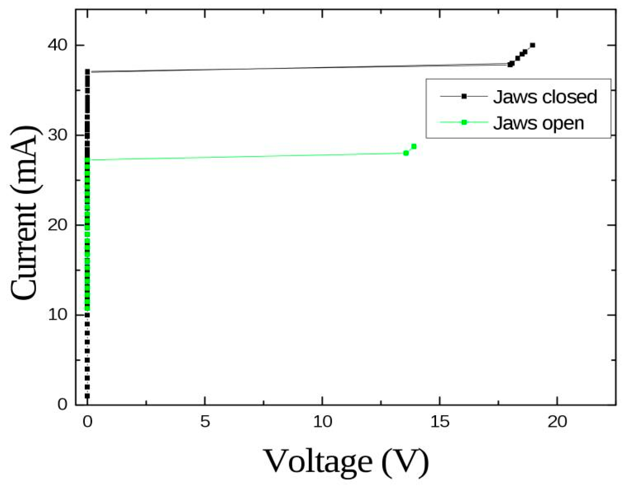
Figure 6.
V-t data for an NbN strip detector. The voltage plateau corresponds to waiting times in the ready state, until an event occurs and a voltage spike is measured. Voltage is measured directly at the strip, with no amplification. (Adapted from [12], with the permission of IOP Publishing).
Figure 6.
V-t data for an NbN strip detector. The voltage plateau corresponds to waiting times in the ready state, until an event occurs and a voltage spike is measured. Voltage is measured directly at the strip, with no amplification. (Adapted from [12], with the permission of IOP Publishing).

© 2018 by the author. Licensee MDPI, Basel, Switzerland. This article is an open access article distributed under the terms and conditions of the Creative Commons Attribution (CC BY) license (http://creativecommons.org/licenses/by/4.0/).
Share and Cite
MDPI and ACS Style
Merlo, V. Superconducting Strips: A Concept in Thermal Neutron Detection. Instruments 2018, 2, 4. https://doi.org/10.3390/instruments2010004
AMA Style
Merlo V. Superconducting Strips: A Concept in Thermal Neutron Detection. Instruments. 2018; 2(1):4. https://doi.org/10.3390/instruments2010004
Chicago/Turabian StyleMerlo, Vittorio. 2018. "Superconducting Strips: A Concept in Thermal Neutron Detection" Instruments 2, no. 1: 4. https://doi.org/10.3390/instruments2010004