Article

Monolithically-Integrated Single-Photon Avalanche Diode in a Zero-Change Standard CMOS Process for Low-Cost and Low-Voltage LiDAR Application

1
Hewlett Packard Labs, Hewlett Packard Enterprise, Palo Alto, CA 94304, USA
2
Center for Optoelectronic Materials and Devices, Korea Institue of Science and Technology (KIST), Seoul 02792, Korea
*
Author to whom correspondence should be addressed.
Instruments 2019, 3(2), 33; https://doi.org/10.3390/instruments3020033
Submission received: 30 April 2019 / Revised: 20 June 2019 / Accepted: 21 June 2019 / Published: 25 June 2019
(This article belongs to the Special Issue Single-Photon Detection Instrumentation and Applications)

Abstract

:
We present a single-photon sensor based on the single-photon avalanche diode (SPAD) that is suitable for low-cost and low-voltage light detection and ranging (LiDAR) applications. It is implemented in a zero-change standard 0.18-μm complementary metal oxide semiconductor process at the minimum cost by excluding any additional processing step for customized doping profiles. The SPAD is based on circular shaped P+/N-well junction of 8-μm diameter, and it achieves low breakdown voltage below 10 V so that the operation voltage of the single-photon sensor can be minimized. The quenching and reset circuit is integrated monolithically to capture photon-generated output pulses for measurement. A complete characterization of our single-photon sensor is provided.

1. Introduction

Light detection and ranging (LiDAR) has attracted significant research and development interest over recent years as demands for three-dimensional (3D) imaging technologies have increased in various fields including automotive vehicles, drones, robots, and many other scientific, medical and consumer applications [1,2]. Among others, single-photon avalanche diode (SPAD) technology is a critical building block of such LiDAR systems as it can simultaneously improve sensitivity and timing accuracy [3]. Especially, SPADs implemented in a standard complementary metal oxide semiconductor (CMOS) process is the key that enables high-volume production of low-cost single-photon sensors. Although many efforts have been focusing on realizing CMOS-compatible SPADs and single-photon sensors in deep-submicron CMOS technology [4,5,6,7,8,9,10,11,12,13,14,15,16], the majority of them rely on non-standard processes with customized layers that increase the cost and design complexity.
In this article, we present a SPAD-based single-photon sensor that is suitable for low-cost and low-voltage LiDAR systems in mobile devices and automotive vehicles. Our sensor is fully compatible with a standard 0.18-μm CMOS process where our SPAD and active quenching and reset circuit (AQRC) are monolithically integrated at the minimum cost as it excludes any of additional processing step for customized doping profile. Our sensor is carefully designed to minimize the operation voltage without sacrificing a significant amount of performance. We provide a full characterization including current-voltage characteristics, dark-count rate (DCR), afterpulsing probability, photon detection probability (PDP), and photon timing jitter.

2. Single-Photon Sensor

Figure 1a,b shows the microscope image of the SPAD-based single-photon sensor and the cross-sectional view of SPAD, respectively, which is fabricated in standard 180 nm CMOS technology (1P6M mixed-signal and RF applications) from TSMC. Our SPAD is based on a P+/N-well junction in a circular shape, and the diameter is 8 μm. P-well guard-ring that has 2-μm width surrounds the junction to protect the device from premature breakdown at the device perimeter, which can be confirmed by a light emission test at 15 V of reverse bias voltage as shown in Figure 1a. An additional shallow-trench isolation (STI) guard-ring is implemented outside of the P-well guard-ring to prevent lateral tunneling in between P+ and N+ contact regions. However, such STI may dramatically increase the density of deep-level carrier generation centers at its interface, especially when it is located close to the multiplication region of SPAD [17]. For this reason, the STI is located outside the P-well guard-ring to make sure that only a negligible amount of defect contributes to the noise of SPAD and its size is minimized to have a better fill factor. The deep N-well layer implemented beneath the junction not only connects the contact regions for the cathode but also extends the photon-absorption region into deeper silicon substrate so that more carriers generated from photons at near-infrared (NIR) wavelengths are captured and achieves higher PDP. The sensor occupies 20 μm × 40 μm of area in total and the active area of SPAD is 50.24 μm2, which results in 6.3% of fill-factor for a single pixel. Such a fill factor is expected to improve by the factor of two or more for a linear or two-dimensional array by sharing deep the N-well of the adjacent SPADs and optimizing the circuit design. The fill factor can be further improved by using micro lenses [18].
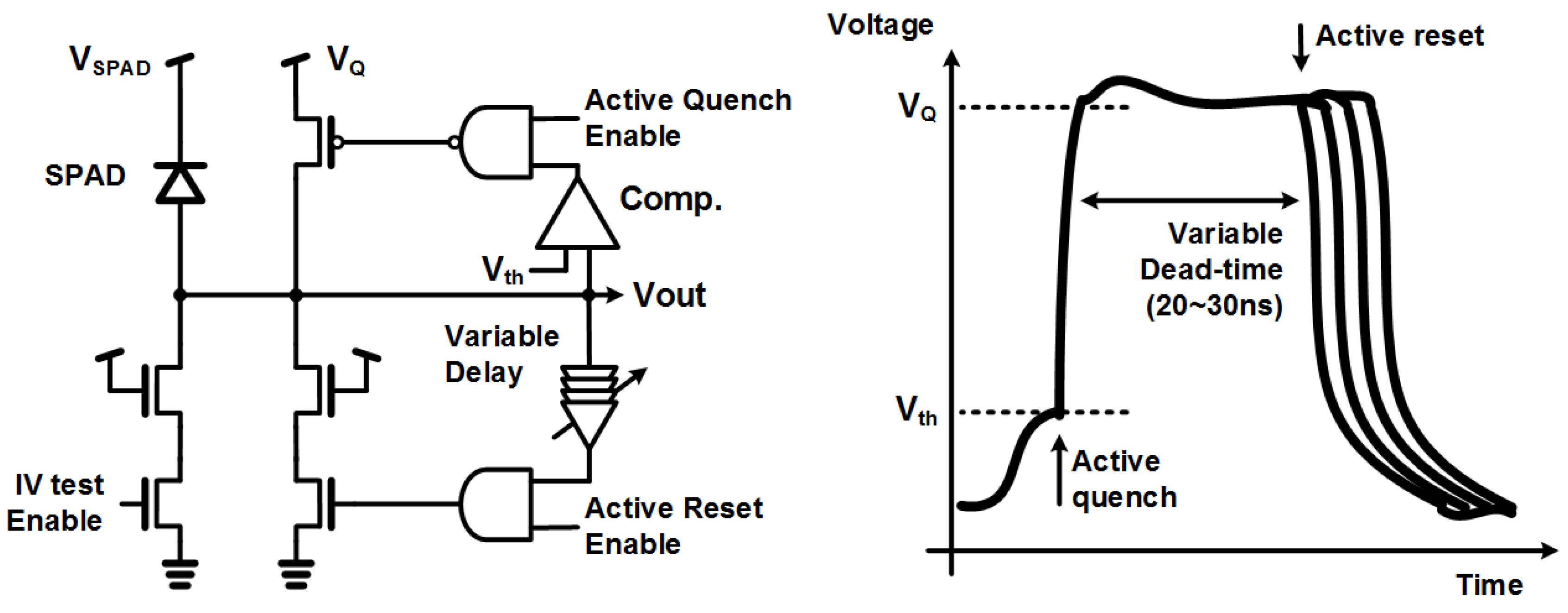
Figure 2 illustrates the circuit diagram of our AQRC and the output waveform of the SPAD. For Geiger-mode operation, reverse bias voltage beyond its breakdown is applied to the cathode of the SPAD while the anode is connected to the AQRC so that output pulses of the SPAD are properly shaped and then provided to field programmable gate arrays (FPGA) or other equipment for measurement. For an active quenching operation, a p-type transistor and a strong-arm latch-based comparator form a closed loop so that the anode of SPAD is quickly charged to the quenching voltage (VQ) through the PMOS transistor once it gets larger than the threshold voltage (Vth) of the comparator. Such anode voltage then turns on the n-type transistor for an active reset operation after some period of time, which is known as the dead-time of the sensor, and it can vary from 20 to 30 ns by a programmable delay line. The AQRC is implemented with 3.3 V I/O transistors with a thick gate to withstand large overdrive voltages that comes from the reverse bias voltage of the SPAD for Geiger-mode operation.

3. Measurement Results

Figure 3 shows IV characteristics of our SPAD under the dark condition at different temperatures, and the inset plots the temperature dependency of the breakdown voltage (VBR). The AQRC is disabled when measuring the IV characteristics, and the amount of current flowing through the diode is integrated for a few milliseconds. Our SPAD exhibits a dark current of 100 pA in range before breakdown and the current increases abruptly at the reverse bias voltage of 9.98 V on average at 300 K, where the variation is less than 10 mV within 32 measured devices. Such low VBR is achieved due to the higher doping concentration level of N-well than deep N-well for given CMOS technology, and it is critical for minimizing the operation voltage of the target LiDAR systems. VBR linearly increases from 9.9 to 10.14 V as the temperature varies from 290 to 320 K as inset shows, and the resulting temperature coefficient of 8 mV/K indicates a weak dependence on the temperature.
Figure 4a shows normalized DCR values as a function of excess bias voltage (Vex), which is the difference between applied reverse bias and breakdown voltage, at different temperatures. The normalized DCR increases from 1.3 to 10.3 kcps/μm2 at 300 K as Vex changes from 1 to 2 V and such strong exponential dependence of DCR on Vex is an indication that band-to-band tunneling is a dominant contributor of DCR rather than Shockley–Read–Hall recombination or thermal generation. This can be confirmed with low activation energy levels (Ea) extracted from the Arrhenius plot shown in Figure 4b where the values are 0.114, 0.161, and 0.197 eV for Vex of 1, 1.5, and 2 V, respectively, and the corresponding determination coefficients (R2) are 0.995, 0.997, and 0.999, respectively. It should be noted that DCR of our SPAD is relatively larger than some of the SPADs implemented in advanced CMOS processes, but it is still in the acceptable range for the target LiDAR systems where the background ambient light is the dominant noise [19]. In addition, such advanced processes not only increase the fabrication cost but also the operation voltage, which is more critical to the target LiDAR systems.
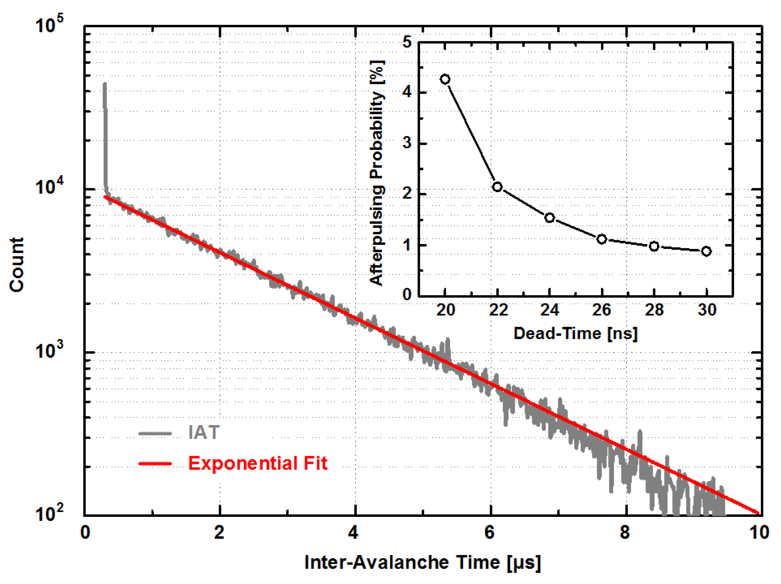
Figure 5 plots the histogram of inter-avalanche times (IATs) under the dark condition with a fitted exponential curve and the inset shows the dependence of afterpulsing probability on the dead-time of the sensor. The histogram of primary dark counts are known to follow an ideal Poisson distribution [20] and, therefore, the afterpulsing probability is statistically derived by taking the fraction of IATs that deviate from an ideal exponential distribution. Our SPAD exhibits afterpulsing probability of 4.3% with Vex of 2 V when the dead-time is 20 ns, and it can be reduced to less than 1% by increasing the dead-time to 30 ns.
Figure 6 shows the PDP of the SPAD as a function of wavelength at different Vex. For this measurement, a Xenon light source with a monochromator (DMC1-04 from Optometrics) is used to select the wavelength of the light and radiate it into an integrating sphere (IS200 from Thorlabs) and the reference photodiode (S130C from Thorlabs) is used to calculate PDP. The maximum PDP of our SPAD is 30.4% at the wavelength of 535 nm and Vex of 2 V. Although PDP decreases with wavelengths as photon penetration depth starts to exceed the depth of P+/N-well junction, our SPAD still achieves as high a PDP as 5.6% and 3.8% at 850 and 905 nm, respectively. This is mainly due to the deep N-well implemented beneath the junction that extends the photon-absorption region into deeper substrate where more photons of longer wavelengths are absorbed and contribute to avalanche multiplication process. Our SPAD achieves better or comparable PDP than others fabricated in non-standard processes in similar technology nodes. Such NIR-enhanced PDP characteristics are critical for LiDAR applications as many of them operate at 850 or 905 nm because of silicon compatibility, minimum absorption at free-space by water, and eye-safety issues [21].
Figure 7 shows a normalized histogram of time response based on time-correlated single-photon counting (TCSPC) technique, and the inset plots timing jitter, full-width at half-maximum (FWHM), as a function of Vex. For this measurement, a LiDAR demonstration board (EPC9126 from EPC) that consists of ground-referenced enhanced GaN field effect transistor driven by a gate driver (LMG1020 from Texas Instruments) and 905 nm pulsed laser diode (DPGEW1S09H from Excelitas) were used. The measured timing jitter is 110 ps at Vex of 1 V, and it can be further improved to 92 ps with Vex of 2 V including the contribution from the laser diode, which corresponds to a depth resolution of 3 cm for the time-of-flight measurement, and such small jitter is mainly due to the sharp transition of the monolithically-integrated AQRC.
The performance of our SPAD is summarized in Table 1 and compared with other SPADs implemented in standard CMOS technologies. Although our SPAD has higher DCR, it achieves the lowest VBR and the shortest dead-time while exhibiting better or comparable PDP, afterpulsing probability, and timing jitter at the target wavelength of 905 nm.

4. Conclusions

In conclusion, a monolithically-integrated single-photon sensor fabricated in a zero-change standard 0.18-μm CMOS process is presented and characterized. It should be emphasized that our SPAD uses none of the additional processing steps to minimize the cost and is carefully designed to minimize the operation voltage without significant performance degradation. We expect our sensor to play a critical role in realizing single-photon sensors for low-cost and low-voltage LiDAR applications.

Author Contributions

Conceptualization, J.R. and M.-J.L.; methodology, J.R.; software, X.Z., Z.H. and S.R.C.; validation, J.R. and M.-J.L.; writing—original draft preparation, J.R.; writing—review and editing, J.R. and M.-J.L.; supervision, M.F. and R.B.

Funding

This research received no external funding.

Conflicts of Interest

The authors declare no conflict of interest.

References

  1. Hadfield, R.H. Single-photon detectors for optical quantum information applications. Nat. Photon. 2009, 3, 696–705. [Google Scholar] [CrossRef]
  2. Bruschini, C.; Homulle, H.; Charbon, E. Ten years of biophotonics single-photon SPAD imager applications – retrospective and outlook. In Proceedings of the Advanced Photon Counting Techniques XI, Anaheim, CA, USA, 9–13 April 2017. [Google Scholar]
  3. Ghioni, M.; Gulinatti, A.; Rech, I.; Zappa, F.; Cova, S. Progress in silicon single-photon avalanche diodes. IEEE J. Sel. Topics Quantum Electron. 2007, 13, 852–862. [Google Scholar] [CrossRef]
  4. Lee, M.-J.; Sun, P.; Charbon, E. A first single-photon avalanche diode fabricated in standard SOI CMOS technology with a full characterization of the device. Opt. Express 2015, 23, 13200–13209. [Google Scholar] [CrossRef] [PubMed]
  5. Pellegrini, S.; Rae, B. Fully industrialised single photon avalanche diodes. In Proceedings of the Advanced Photon Counting Techniques XI, Anaheim, CA, USA, 9–13 April 2017. [Google Scholar]
  6. Pellegrini, S.; Rae, B.; Pingault, A.; Golanski, D.; Jouan, S.; Lapeyre, C.; Mamdy, B. Industrialised SPAD in 40 nm Technology. In Proceedings of the 2017 IEEE International Electron Devices Meeting (IEDM), San Francisco, CA, USA, 2–6 December 2017. [Google Scholar]
  7. Niclass, C.; Soga, M.; Matsubara, H.; Kato, S.; Kagami, M. A 100-m range 10-frame/s 340x96-pixel time-of-flight depth sensor in 0.18-μm CMOS. IEEE J. Solid-State Circuits 2013, 48, 559–572. [Google Scholar] [CrossRef]
  8. Niclass, C.; Gersbach, M.; Henderson, R.; Grant, L.; Charbon, E. A single photon avalanche diode implemented in 130-nm CMOS technology. IEEE J. Solid-State Circuits 2007, 13, 863–869. [Google Scholar] [CrossRef]
  9. Karami, M.A.; Gersbach, M.; Yoon, H.-J.; Charbon, E. A new single-photon avalanche diode in 90nm standard CMOS technology. Opt. Express 2010, 18, 22158–22166. [Google Scholar] [CrossRef] [PubMed]
  10. Huang, L.D.; Wu, J.Y.; Wang, J.P.; Tsai, C.M.; Huang, Y.H.; Wu, D.R.; Lin, S.D. Single-photon avalanche diodes in 0.18-μm high-voltage CMOS technology. Opt. Express 2017, 25, 13333–13339. [Google Scholar] [CrossRef] [PubMed]
  11. Webster, E.A.G.; Grant, L.A.; Henderson, R.K. A high- performance single-photon avalanche diode in 130-nm CMOS imaging technology. IEEE Electron Device Lett. 2012, 33, 1589–1591. [Google Scholar] [CrossRef]
  12. Veerappan, C.; Charbon, E. CMOS SPAD based on photo-carrier diffusion achieving PDP > 40% from 440 to 580 nm at 4V excess bias. IEEE Photon. Technol. Lett. 2015, 27, 2445–2448. [Google Scholar] [CrossRef]
  13. Xu, H.; Pancheri, L.; Betta, G.-F.D.; Stoppa, D. Design and characterization of a p+/n-well SPAD array in 150nm CMOS process. Opt. Express 2017, 25, 12765–12778. [Google Scholar] [CrossRef] [PubMed]
  14. Faramarzpour, N.; Deen, M.J.; Shirani, S.; Fang, Q. Fully integrated single photon avalanche diode detector in standard CMOS 0.18-μm technology. IEEE Tran. Electron Devices 2008, 55, 760–767. [Google Scholar] [CrossRef]
  15. Pancheri, L.; Stoppa, D. Low-noise single photon avalanche diodes in 0.15 μm CMOS technology. In Proceedings of the 2011 European Solid-State Device Research Conference (ESSDERC), Helsinki, Finland, 12–16 September 2011. [Google Scholar] [CrossRef]
  16. Palubiak, D.P.; El-Desouki, M.M.; Marinov, O.; Deen, M.J.; Fang, Q. High-speed, single photon avalanche photodiode imager for biomedical applications. IEEE Sens. J. 2011, 11, 2401–2412. [Google Scholar] [CrossRef]
  17. Finkelstein, H.; Hsu, M.J.; Esener, S. STI-bounded single-photon avalanche diode in a deep-submicrometer CMOS technology. IEEE Electron Device Lett. 2006, 27, 887–889. [Google Scholar] [CrossRef]
  18. Pavia, J.M.; Wolf, M.; Charbon, E. Measurement and modeling of microlenses fabricated on single-photon avalanche diode arrays for fill factor recovery. Opt. Express 2014, 22, 4202–4213. [Google Scholar] [CrossRef] [PubMed]
  19. Katz, A.; Eshkoli, A.; Feningstein, A.; Jackson, C.; Nemirovsky, Y. Design considerations of CMOS Si photomultiplier for long range LIDAR. In Proceedings of the 2017 IEEE International Conference on Microwaves, Antennas, Communications and Electronic Systems (COMCAS), Tel Aviv, Israel, 13–15 November 2017. [Google Scholar]
  20. Palubiak, D.P.; Li, Z.; Deen, M.J. Afterpulsing characteristics of free-running and time-gated SPADs in 130nm CMOS. IEEE Tran. Electron Devices 2015, 62, 3727–3733. [Google Scholar] [CrossRef]
  21. Williams, G.M. Optimization of eyesafe avalanche photodiode lidar for automobile safety and autonomous navigation systems. Optical Eng. 2017, 56. [Google Scholar] [CrossRef]
Figure 1. (a) Microscope image of the fabricated single-photon sensor and the light emission test result; (b) Cross-sectional view of a single-photon avalanche diode (SPAD).
Instruments 03 00033 g001
Figure 2. Circuit diagram of an active quenching and reset circuit (AQRC) and the simulated output waveform.
Instruments 03 00033 g002
Figure 3. IV characteristics of SPAD. Inset plots temperature dependence of excess bias voltage (Vex).
Instruments 03 00033 g003
Figure 4. (a) Normalized dark-count rate (DCR) as a function of Vex at different temperatures; (b) Arrhenius plot with extracted activation energy and determination coefficient for the curve fit (dotted line).
Instruments 03 00033 g004
Figure 5. Histogram of inter-avalanche times (IAT) with exponential fit. Inset shows the dead-time dependency of afterpulsing probability.
Instruments 03 00033 g005
Figure 6. Photon detection probability (PDP) values as a function of wavelength at different Vex.
Instruments 03 00033 g006
Figure 7. Time response of SPAD. Inset shows the dependency of Vex on the timing jitter (full-width at half-maximum (FWHM)).
Instruments 03 00033 g007
Table 1. Performance summary and comparison.
This Work[13][14][15][16][10][11]
Technology0.18-μm 0.15-μm0.18-μm0.15-μm0.13-μm0.18-μm0.13-μm
ProcessStandard CMOSStandard CMOSStandard CMOSStandard CMOSStandard CMOSHigh-Voltage CMOSCMOS Image Sensor
Junction
Structure
P+/
N-well
P+/
N-well
P+/
N-well
P+/
N-well
N+/
P-well
Deep P-well/
Buried-N
Deep N-well/
P-sub
Guard-Ring
Structure
P-wellDeep
N-well
P-wellP epiN-wellP-wellP-epi
Virtual
Active
Area
50.24 μm297.12 μm290 μm278.5 μm2100 μm2100 μm216 μm2
ShapeCircleSquareOctagonCircleSquareCircularCircular
VBR9.98 V18.01V10.2 V16.1 V11.3 V49.9 V20 V
Vex2 V3 V2 V3.5 V2.2 V5 V2 V
Normalized
DCR
10300 cps/μm20.4 cps/μm27780 cps/μm2
@ 0.5 Vex
1.53 cps/μm21000 cps/μm20.68 cps/μm21.125 cps/μm2
Afterpulsing
Probability
(Dead Time)
1%
(30 ns)
0.85%
(150 ns)
N/A0.45%
(100 ns)
N/A1.6%
(20 ns)
4%
@ 12Vex
(N/A)
PDP Peak
(λ)
30.4%
(530 nm)
27.5%
(450 nm)
5.5%
(450 nm)
25%
(470 nm)
13%
(570 nm)
22%
(570 nm)
72%
@ 12Vex
(550 nm)
PDP
@ 905 nm
3.8%2%N/AN/AN/A2.8%5%
FWHM
Timing Jitter
(λ)
92 ps
(905 nm)
42 ps
@ 4Vex
(831nm)
N/A92 ps
(470 nm)
N/A200 ps
(720 nm)
N/A