Article

Response of G-NUMEN LaBr3(Ce) Detectors to High Counting Rates

by
Elisa Maria Gandolfo
1,2,
José Roberto Brandao Oliveira
3,
Luigi Campajola
1,2,
Dimitra Pierroutsakou
2,
Alfonso Boiano
2,
Clementina Agodi
4,
Francesco Cappuzzello
4,5,
Diana Carbone
4,
Manuela Cavallaro
4,
Irene Ciraldo
4,
Daniela Calvo
6,
Franck Delaunay
4,5,7,
Canel Eke
8,
Fabio Longhitano
9,
Nilberto Medina
10,
Mauricio Moralles
10,
Diego Sartirana
6,
Vijay Raj Sharma
11,
Alessandro Spatafora
4,
Dennis Toufen
12 and
Paolo Finocchiaro
4,* for the NUMEN Collaboration
add Show full author list remove Hide full author list
1
Department of Physics “Ettore Pancini”, University of Napoli Federico II, 80138 Napoli, Italy
2
INFN—Sezione di Napoli, 80126 Napoli, Italy
3
Instituto de Física, Universidade de São Paulo, São Paulo 05508-070, SP, Brazil
4
INFN—Laboratori Nazionali del Sud, 95123 Catania, Italy
5
Department of Physics and Astronomy “Ettore Majorana”, University of Catania, 95124 Catania, Italy
6
INFN—Sezione di Torino, 10125 Torino, Italy
7
LPC Caen UMR 6534, Université de Caen Normandie, ENSICAEN, CNRS/IN2P3, F-14000 Caen, France
8
Department of Mathematics and Science Education, Faculty of Education, Akdeniz University, 07058 Antalya, Turkey
9
INFN—Sezione di Catania, 95125 Catania, Italy
10
Instituto de Pesquisas Energéticas e Nucleares, IPEN/CNEN, São Paulo 05508-000, SP, Brazil
11
Department of Radiation Oncology, University of Maryland, Baltimore, MD 21201, USA
12
Federal Institute of Education, Science and Technology of São Paulo, Guarulhos 07115-000, SP, Brazil
*
Author to whom correspondence should be addressed.
Instruments 2023, 7(3), 28; https://doi.org/10.3390/instruments7030028
Submission received: 5 July 2023 / Revised: 12 September 2023 / Accepted: 14 September 2023 / Published: 16 September 2023

Abstract

:
The G-NUMEN array is the future gamma spectrometer of the NUMEN experiment (nuclear matrix element for neutrinoless double beta decay), to be installed around the object point of the MAGNEX magnetic spectrometer at the INFN-LNS laboratory. This project aims to explore double-charge exchange (DCE) reactions in order to obtain crucial information about neutrinoless double beta decay (0νββ). The primary objective of the G-NUMEN array is to detect the gamma rays emitted from the de-excitation of the excited states that are populated via DCE reactions with a good energy resolution and detection efficiency, amidst a background composed of the transitions from competing reaction channels with far higher cross sections. To achieve this, G-NUMEN signals will be processed in coincidence with those generated by the detection of reaction ejectiles by the MAGNEX focal plane detector (FPD). Under the expected experimental conditions, G-NUMEN detectors will operate at high counting rates, of the order of hundreds of kHz per detector, while maintaining excellent energy and timing resolutions. The complete array will consist of over 100 LaBr3(Ce) scintillators. Initial tests were conducted on the first detectors of the array, allowing for the determination of their performance at high rates.

1. Introduction

Understanding the nature of neutrinos is one of the major open quests in physics beyond the Standard Model. Among the various approaches to this topic, neutrinoless double beta decay (0νββ) is a unique tool to verify if neutrinos are Majorana particles. In principle, the partial half-life, together with the nuclear matrix elements (NMEs), of this decay should allow for the determination of the effective Majorana neutrino mass. However, the current theoretical calculations and experimental attempts to determine NMEs are not yielding conclusive results [1].
The NUMEN project proposes a new approach to this challenge. It aims to obtain information on the NMEs of the 0νββ decay through the study of heavy-ion-induced double-charge exchange (DCE) reactions [2,3,4,5,6]. This approach is based on theoretical analogies between the 0νββ decay and DCE reactions, which were extensively investigated in a previous work [7] and which strongly support the correlation between these two reactions and the development of DCE-constrained theories for the NMEs of the 0νββ decay.
The NUMEN project focuses on exploring DCE reactions for both the isospin-lowering (τ-τ-) and isospin-rising (τ+τ+) directions, in analogy with the β-β- and β+β+ decays. From a long-term perspective, this study involves several 0νββ decay candidate isotopes as targets such as 76Ge, 82Se, 110Pd, 124Sn, 116Cd, 130Te, and 136Xe and the heavy-ion beams of 18O8+ for β+β+ and of 20Ne10+ for β-β-, with energies ranging from 5 to 60 AmeV. In the explored collisions, other reactions compete with the DCE channel such as the multi-nucleon transfer [8,9,10], single-charge exchange [11,12], and elastic and inelastic channels [13,14,15], in addition to deep inelastic, fusion–fission, fusion evaporation, and other processes, with cross sections of up to several orders of magnitude higher than those of the DCE. Indeed, the main experimental challenge for NUMEN lies in the few nb cross sections expected for DCE reactions [16] and the consequent need for a high-performance detection apparatus with a high sensitivity and resolution and excellent discrimination capabilities. Such an apparatus is currently under development [17].
The detection apparatus comprises the high-acceptance MAGNEX spectrometer, together with its focal plane detector (FPD) [18,19,20], and the G-NUMEN array, consisting of 110 LaBr3(Ce) scintillators placed around the target area (Figure 1) [5,21,22].
MAGNEX can detect DCE events with excellent selectivity [23]. Its energy resolution is normally sufficient for the separation of low-lying energy states involving non-deformed nuclei in experiments with low-energy beams, while the G-NUMEN array will be crucial for all situations involving high-energy beams and deformed target nuclei, for which the resolution of MAGNEX is not enough to separate the nearby states of the residual nuclei under study. In these cases, the DCE states are identified by time coincidence and anti-coincidence between the MAGNEX focal plane charged-particle detectors (FPD) and the characteristic gamma-ray transitions detected by G-NUMEN. Indeed, in a typical G-NUMEN experiment, an almost continuum gamma-ray spectrum is expected, and identifying the DCE gamma transition lines requires the coincidence with MAGNEX, according to detailed GEANT4 simulations [5].
The main LaBr3(Ce) characteristics of interest for NUMEN, besides its radiation hardness, particularly for fast neutrons, are the high light output, the excellent energy resolution, and the fast time response that fit the very strict demands for the G-NUMEN array. The most important demands are a time resolution of a few ns in order to be able to distinguish between subsequent beam bunches (occurring every 30–50 ns) and to reject a very intense random coincidence background, and an energy resolution better than 10% at 200 keV, enough to separate the first and second excited states of the nuclei under study [5].
Extensive examples can be found in the literature about the crystal characterization and its scintillation properties under the condition of the standard detection rate [24,25,26,27,28]. However, due to the extreme experimental conditions foreseen for the reactions involving G-NUMEN, simulations show that the G-NUMEN array will be exposed to an intense radiation background of both neutrons and gammas, resulting in detection rates of up to 300 kHz for each scintillator [5]. In the literature, there are studies on the response of LaBr3(Ce) detectors to high detection rates [29,30], and numerous studies address the problem of the stability of the phototube under the conditions of a high rate and linearity issues [31,32,33,34,35,36]. However, the challenging experimental environment of NUMEN requires further characterization of the scintillators’ performance in order to deeply understand the response of the array under such detection rates, in particular their energy resolution, their linearity, and the optimal electronic setup for signal processing.
This work focuses on the characterization and testing of the first prototypes of G-NUMEN scintillators, evaluating their performance under the foreseen detection rate for the NUMEN experiment. Different electronic systems for signal acquisition are assessed with the purpose of identifying the most suitable setup for the future experimental conditions. Specifically, we test two commercially available bases (one active and one passive) for the LaBr3(Ce)-crystal-coupled phototubes. We also report the results of the simulation of the phototube and its active base. We show here that the simulations are essential for optimizing the design of a new active base that will satisfy the requirements of the NUMEN project.

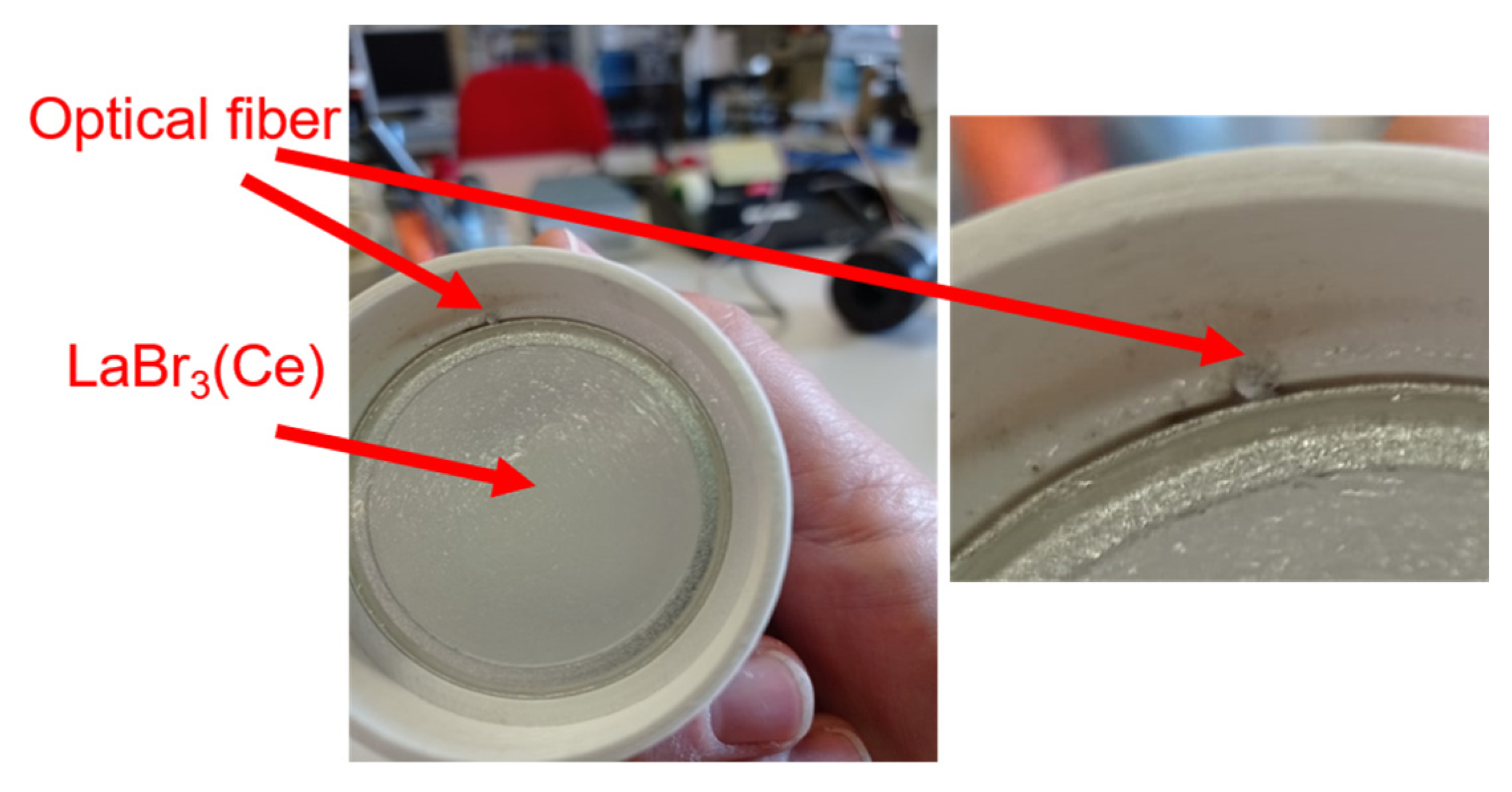
2. Materials and Methods

The material, geometry, and dimensions of the G-NUMEN scintillator array were carefully selected to optimize timing, efficiency, energy resolution, and signal-to-noise ratio, while also adapting to various mechanical constraints. Each scintillator consists of a LaBr3(Ce) crystal (Φ = 38 mm diameter, l = 50 mm length) with light that is collected by an 8-dynode-stage PhotoMultiplier Tube (PMT). The PMT is the R6231 model from Hamamatsu, while the crystals are produced by EPIC-Crystal (China). Figure 2 shows a typical spectrum obtained with a 22Na source that produces gamma rays of 511 and 1275 keV. Also shown is the channel-to-energy linear calibration plot, produced using the data in Table 1.
Figure 3 shows the prototype of one shell of the gamma array and the typical background spectrum, with prominence of the internal radioactivity of the detectors. To assess the performance of the scintillators, key parameters such as energy resolution, efficiency, gain, and linearity were evaluated. Calibration sources such as 22Na, 60Co,137Cs, and 152Eu as well as the internal activity peaks of the crystal at 35.5 keV and 1472 keV were used for this purpose [26,28].
The characteristics of the scintillators were tested at increasing detection rates to obtain a global description of the detectors’ response to counting rates up to the maximum rate foreseen in NUMEN, i.e., ~300 kHz. To reach these high rates, different approaches were employed.
An intense 137Cs radioactive source with activity of 1.5 MBq was used at the INFN-LNS facility and placed at varying distances from the detectors to vary their counting rates. This intense source was used in addition to other calibration sources, with peaks that were analyzed in terms of energy resolution and gain. This allowed for an investigation of the detector response under different levels of counting rate, up to 180 kHz. The detector signal pulses were sent to a CAEN VX2745 16 bit 125 MS/s digitizer, running Pulse Shape Discrimination firmware [37], which allows for integrating the pulse charge in an adjustable time range.
The detectors were also exposed to a fusion–evaporation reaction at the ALTO facility of the IJC Laboratory. This reaction induced high detection rates, up to 310 kHz, and provided additional insights into the scintillators’ performance. In this case, a 22Na calibration source was used as reference, with emitted gamma rays that were detected over the background produced by the fusion–evaporation reaction. The average energy of the background spectrum during these tests was similar to that of typical G-NUMEN DCE experiments, around 400 keV. Indeed, the experiments presented in this work aimed at simulating realistic experimental conditions and evaluating the behavior and response of the scintillators at the anticipated detection rates expected for the NUMEN project.
To explore the compatibility of different electronic configurations with the foreseen experimental environment, the tests were conducted at different supply voltages (HV) using both passive-resistor-type (Hamamatsu E1198-26) and active-type (EPIC Crystal — Model No.: GW-N-N-N-1-N-0) voltage dividers. Indeed, the detector performances, such as linearity and energy resolution, can be affected by the detection rate as well as by the voltage supply and the electronic configuration (i.e., voltage divider type).
The scintillation yield of the LaBr3(Ce) crystals of the various detectors is expected to be very similar, but the quantum efficiency and gain of the photomultipliers, even those of the same model and at the same supply voltage, can be quite different for each individual device. The output pulse charge per gamma-ray energy was observed to significantly vary, at the same applied voltages, among the 15 prototype detectors that were tested. In addition, the performance of the used bases was impacted by the average currents drawn from the PMT. Therefore, it is crucial to perform experimental tests to evaluate the response of the various detectors by varying the voltage bias, the detection rate, and the electronic configurations.

3. Results

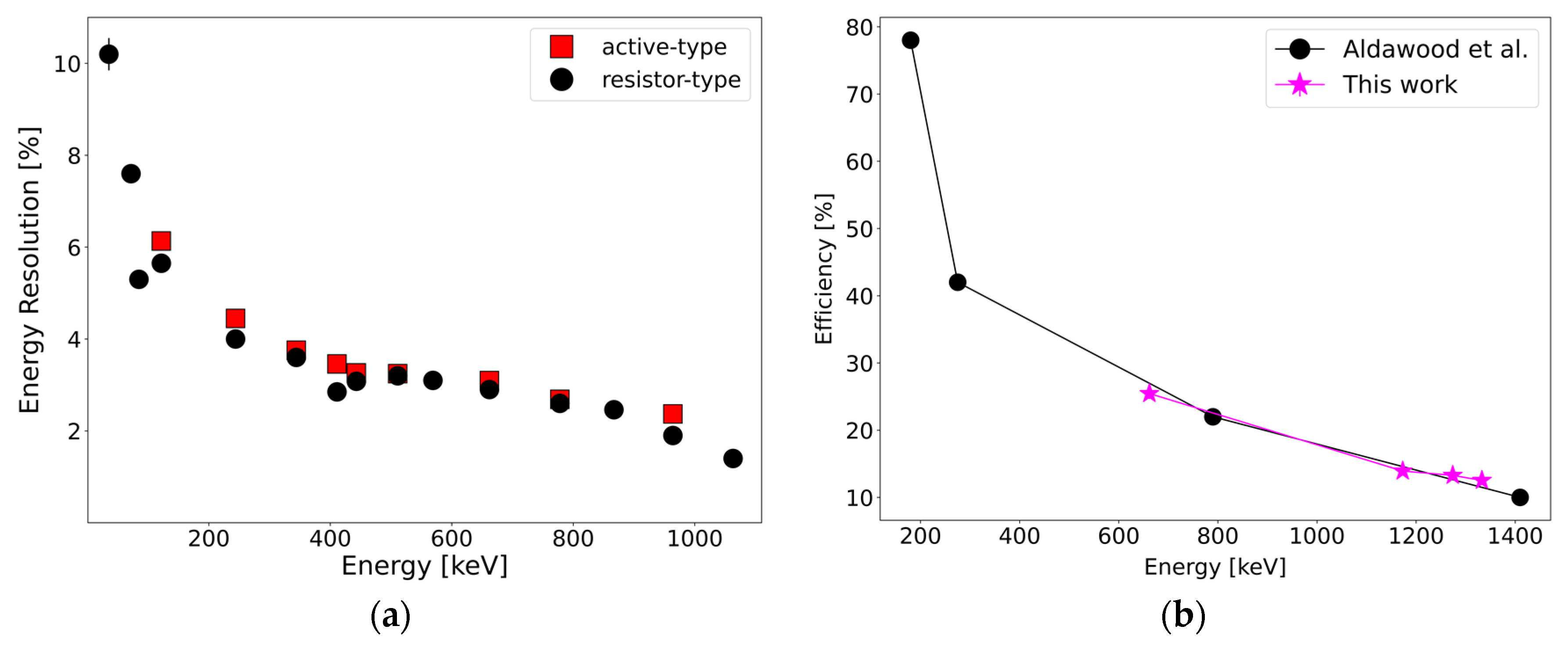
3.1. Energy Resolution and Photopeak Efficiency at Low Rates with Different Base Configurations

The energy resolution and photopeak efficiency of two of the detectors are shown in Figure 4. The data were collected at a fixed voltage (HV = −1000 V) and low detection rate (<10 kHz). Under this condition, these characteristics mainly depend on the crystal; therefore, no changes can be noticed between the results for resistor-type and active-type voltage dividers (i.e., base).

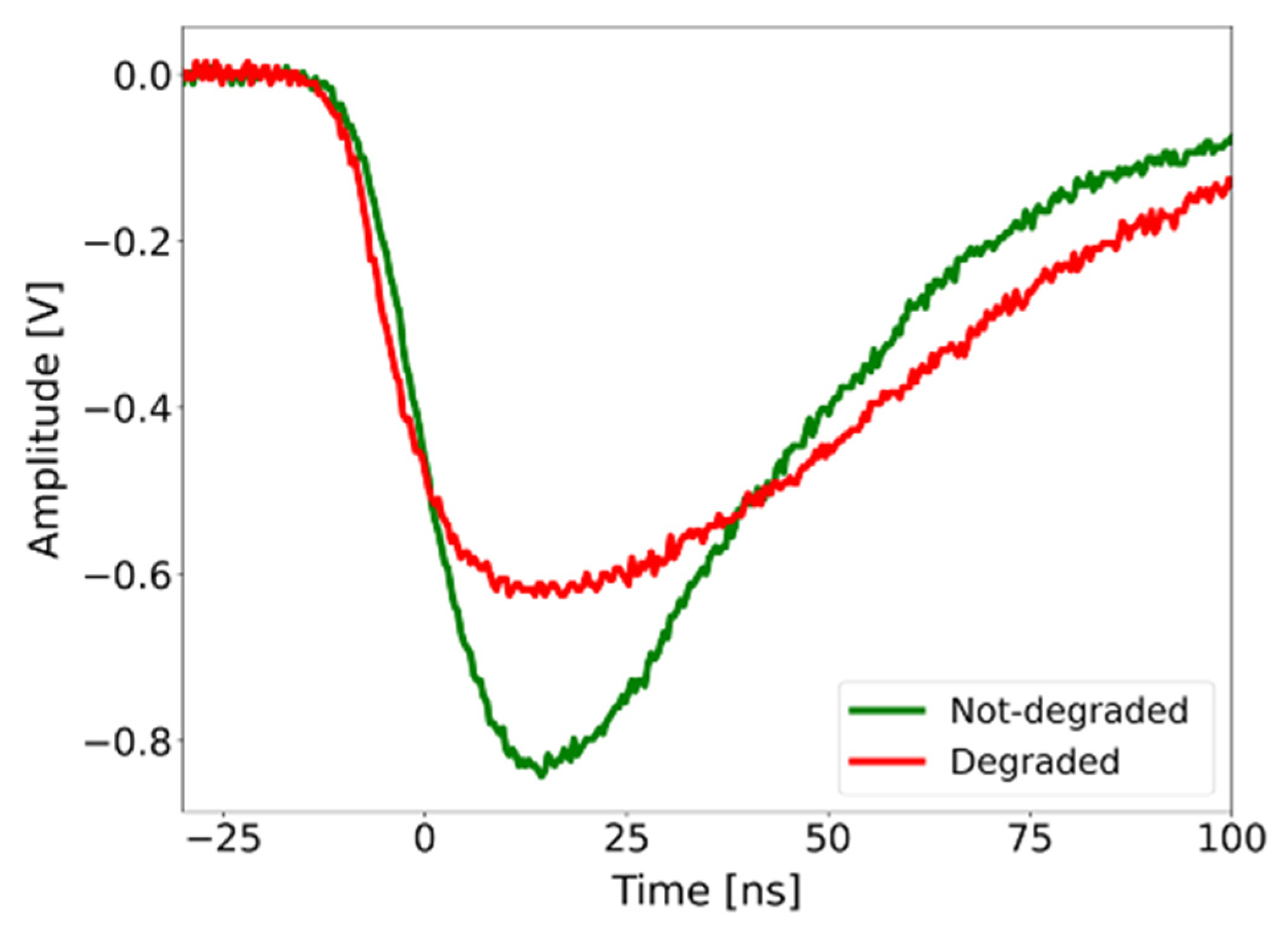
3.2. Gain and Non-Linearity of the Detector Response

The charge conversion gain g can be defined as the ratio between the charge and the energy of a given signal (g = Q/E). This gain (or integral gain) was measured as a function of the detection rate, using an intense 137Cs source (1.5 MBq). For a linear response of the detector, the gain should be constant. The maximum rate reached in this test was RMAX = 180 kHz. The average output anode current can be obtained from the average pulse charge times the count rate (Ia = QavR). An increase in the detection rate represents an increase in the anode current Ia. Figure 5a shows the relative variation in this gain, with the anode current at different energies for both resistor-type and active-type detectors.
It can be noticed that, although both detectors were exposed to the same maximum rate, the maximum anode current is different because the amplification of the two photo-multipliers is already different at a low rate. The detector with a resistor-type voltage divider shows a larger relative gain variation with rate, and a substantial difference in the trend of the gain variation at high energy (2.6 MeV), with respect to the one at a lower energy (662 keV); this behavior indicates an increasing non-linearity of the response with energy as the rate is increased. As expected from the literature [38], the response of the detector with an active-type voltage divider is more stable, with respect to the resistor type at high rates.
It can be useful to introduce the differential gain gij, which allows for the comparison of the conversion gain at different energies, and it can be defined as
g i j = Q j Q i E j E i
where Qj is the integrated pulse charge corresponding to the j-th peak centroid of energy Ej. The differential gain is more sensitive than the integral gain (gj = Qj/Ej) to the non-linearity of the conversion. In particular, the deviation from the unity of the differential gain ratio gij/gni, evaluated for a set of peaks in a given energy range, reflects the non-linearity of the conversion in that energy range.
Figure 5b shows the differential gain ratio for several detectors with the active-type base at energies corresponding to the 1173.2 keV (peak 1) and 1332.5 keV (peak 2) transitions, from a 60Co source, and the 2505.7 keV (peak 3) transition, from the sum peak at a close-distance geometry, all with the same voltage applied to the PMT (−937.5 V). Each data point corresponds to a different detector. The variation in g1 spans a factor larger than three, illustrating a wide spread of the PMT multiplication factor or gain. The drop of gij/gni observed for a large g1 indicates the emergence of a non-linear behavior due to space-charge effects as the pulse charge increases [38]. The PMT gain g, as a function of the applied voltage, can be seen in Figure 6a for two different detectors. Note that at this gamma energy range, both the differential and integral gains are very similar. This dependence can be expressed as
g = p 0 V p 1
where p0 and p1 are the adjustable parameters of a fit to the g versus the V data of a specific detector, such as those shown in Figure 6a.

3.3. Energy Resolution at Different PMT Voltages

Equation (2) allows for the expression of the energy resolution of the detector as a function of the gain instead of the supply voltage, as shown in Figure 6b. The highest gain of each detector is obtained at −1000 V. Both the low-gain PMT detector (red data points) and the large-gain PMT detector (blue data points) present a good resolution (~2%) around the same gain (0.2 pC/keV), rather than at the same voltage. Figure 7 shows a similar plot for different gamma-ray energies, illustrating that roughly the same gain (0.2–0.3 pC/keV) is required for a good resolution at all energies.

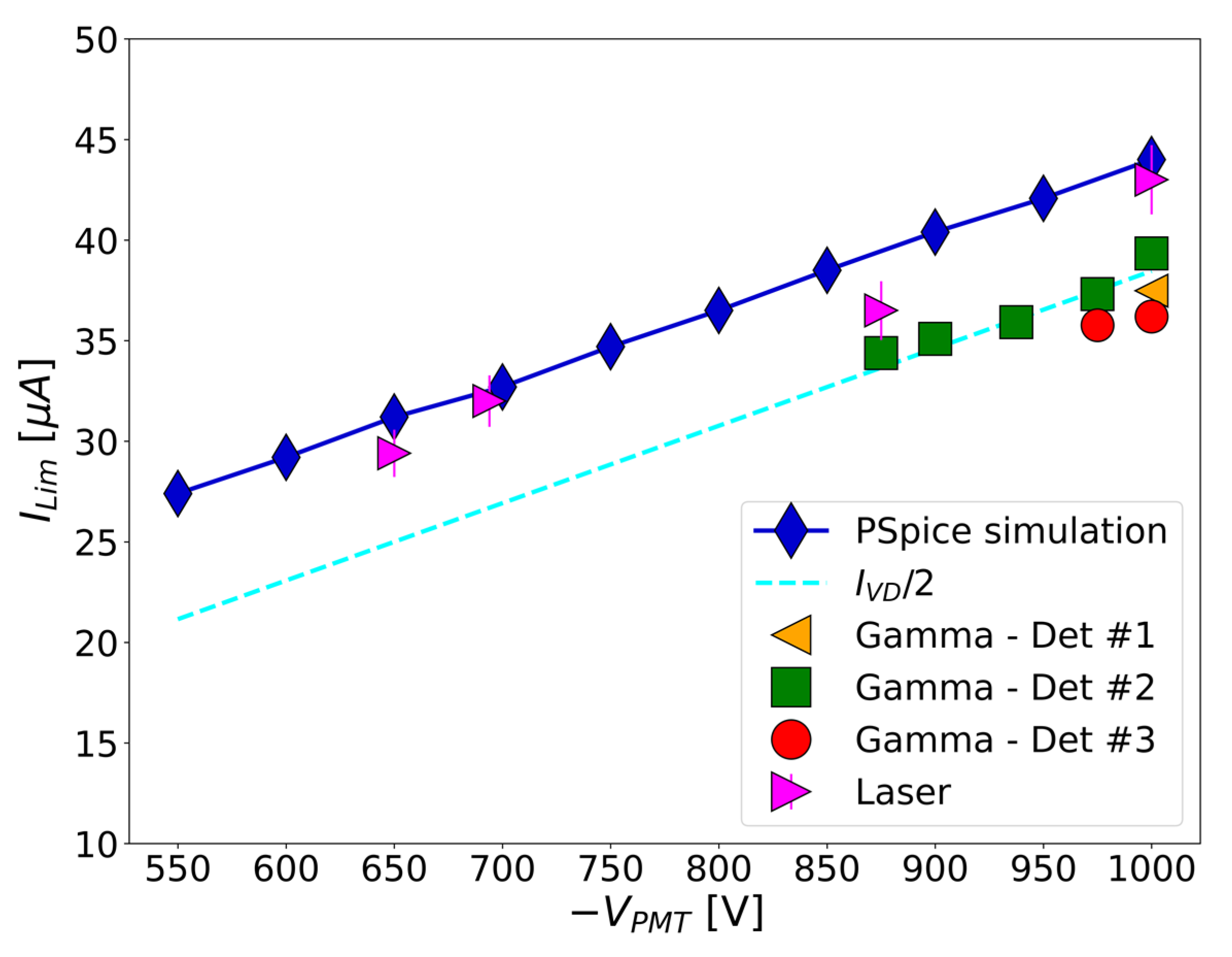
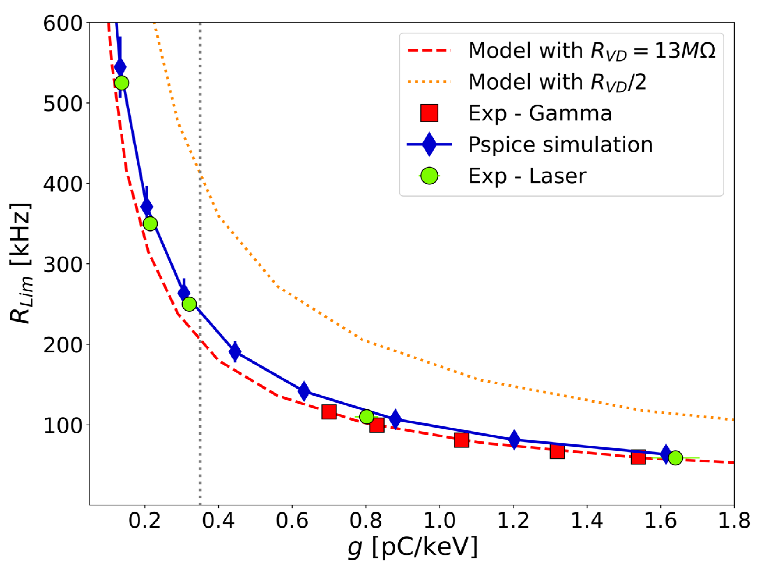
3.4. Limitation in Current

The gain variation in both resistor-type and active-type detectors was measured in conditions similar to those expected in NUMEN, reaching a high detection rate corresponding to a maximum of 180 kHz for the active-type detector and 310 kHz for the passive-type detector. Figure 8a shows the relative gain variation for the two detector types under such counting rates; the latter are expressed in terms of anode current, to be able to compare the different base performances rather independently of the respective PMT gains. The data points in red and black correspond, respectively, to the response of the active-type and the resistor-type base detectors to an intense 137Cs source (max. 180 kHz); the blue points represent the response of the resistor-type detector to the high rate produced during the fusion–evaporation reaction (max. 310 kHz). It can be noticed that the active-type detector shows an abrupt change in gain variation at a rate of ~110 kHz, while the response of the resistor-type detector is smoother. The results shown in Figure 8a are representative of the limitation in counting rate, which is more restrictive for the active-type detector than for the resistor-type detector, as is further discussed in Section 4. However, the passive base presents a stronger dependence of the gain on the rate than the active one, within the latter operational range.
A more detailed response of the gain of the active-type detector is shown in Figure 8b. For all data sets, the same maximum count rate of 180 kHz could be reached, but the rates correspond to different anode currents due to the different gains obtained with the individual PMT of each detector.
The data show that the abrupt change in gain occurs for anode currents in the range of 33–38 μA for this set of detectors and applied voltages, while the corresponding count rates could be very different. This anode current value represents the limit in current IL, after which a sort of “breakdown” of the active base performance is observed. In this work, we refer to the limiting anode current and limiting count rate as the values appearing just before the abrupt gain variation. The gaps in the data points of the current, appearing after the limiting value in Figure 8b, are due to the sudden jump in gain at the breakdown point, as can be clearly seen in Figure 8a. Further discussions on this behavior are presented in Section 4.
Figure 9 shows the waveform of a typical detector signal before and after the limiting current is reached; a clear degradation of the signal can be noticed, with a significant increase in rise and fall times. Also, the energy resolution, which only slightly varies as a function of the count rate below the breakdown, showed a significant degradation just above the breakdown (e.g., from 3.1% below to 4.1% just above the breakdown threshold, for the 662 keV peak of the 137Cs source).

3.5. Systematic Measurements of an Individual PMT with Active Base and Laser Pulses

A laser diode, driven by a CAEN DT5810B Dual Fast Digital Detector Emulator, was used to directly send light to the PMT window by means of an optical fiber, installed sideways with respect to the crystal, without interfering with the LaBr3(Ce) scintillation light (see Figure 10).
This made it possible to emulate the detection of signals corresponding to several gamma-ray energies and count rates. The pulses driving the laser diode were tuned, with the goal of obtaining signal shapes similar to those produced by the gamma-ray detection. The integrated charge was scaled to gamma-ray energy, at specific PMT supply voltages, by calibration with data taken with radioactive sources. At low count rates, low voltage biases, and low gamma-ray energies, this conversion factor is independent of the gamma-ray energy. The laser diode signals were calibrated by means of the simultaneous acquisition of the signals of a 60Co source and of the LaBr3(Ce) internal radioactivity. All the peaks in the spectrum (internal radioactivity, 60Co source, and laser peak) were analyzed in terms of energy resolution and gain.
The detector performance at high rates was determined with a light pulse corresponding to about 430 keV. This energy is similar to both the average energy from the measurements with a gamma source and to the expected average energy from a typical NUMEN experiment. The plot in Figure 11 shows the limiting current of the PMT with the active base used for measurements with the laser, as compared with data obtained with gamma rays (as shown in the previous sections), employing three other detectors. Detectors #1 and #2 in Figure 11 are the same as shown in Figure 8b. The laser data were obtained with a different detector.
For what concerns the laser data, the anode current and, consequently, its limiting value were obtained by two independent methods: a) by directly measuring the anode current of the PMT through a measurement of the anode voltage on the load resistor; b) by charge calibrating the pulses and using the relation I a n o d e = Q l a s e r ·   R l a s e r + Q a v e r a g e ·   R n o _ l a s e r . In the latter relation, Q l a s e r and R l a s e r are the laser charge and the rate of the laser pulse given by the pulse generator, respectively; Q a v e r a g e is the average charge of the spectrum without the laser pulse (given only by the internal radioactivity of the crystal and by the C 60 o source); and R n o _ l a s e r = 800   Hz   is the rate without the laser pulse. It is worth noting that I a n o d e at high rates, where the limiting values can be determined, is completely dominated by the laser pulse current, as R l a s e r provides the most relevant contribution to the final value. The results from the two methods were basically identical.
It can be seen that the limiting current increases with the applied PMT voltage. Similar values are obtained for different detectors with the gamma-ray data, in spite of the different amplification factors of the various individual photomultipliers and conversion gains at different voltages (see also Figure 8b). However, the limiting anode current for the laser data is higher than that of the gamma data by about 6–10%. This might be due to the non-linearity of the response at high gamma energies (the laser data are quasi-monochromatic at high rates) and pile-up events or other systematic errors that remained unnoticed. Further investigations are required to clarify this issue.
The laser measurements also show that the energy resolution at various energies is constant as a function of the rate up to the limiting anode current.

4. Simplified Modeling of the Electronics

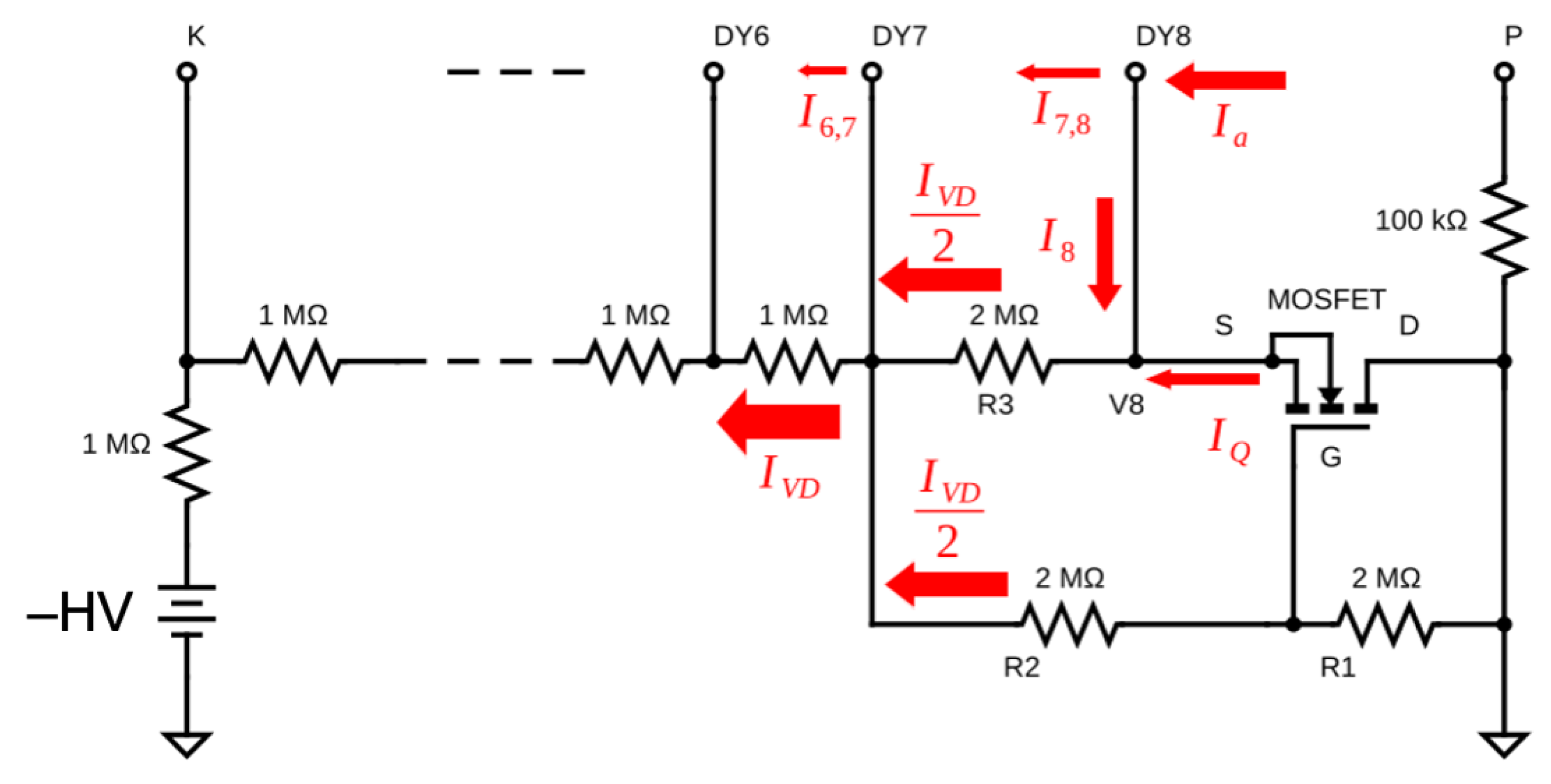
4.1. Active Base Electronic Schematics

In the active base circuit used to distribute the voltage to the PMT dynodes, as shown in Figure 12, only the potential of the last dynode (DY8) is stabilized by a MOSFET transistor (2SK2168) mounted in a source follower. Figure 12 highlights the relevant part of the schematics. The current drawn from the last dynode (I8) added to the one arriving from the MOSFET (IQ) determines the potential drop across the 2 MΩ R3 resistor. As the DY8 current increases, the impedance of the MOSFET also increases, reducing IQ so that the sum (I8 + IQ = IVD/2) is constant, which keeps the potential at the anode (V8) stabilized at only a few volts of difference from the Gate (G) potential, controlled by a voltage divider formed by two 2 MΩ resistors (R1 and R2). The sum of the currents through R2 and R3 continues to the set of 1 MΩ resistors in a series, which forms the rest of the (passive) voltage divider that biases the other dynodes. When IQ reaches zero (the MOSFET is in cutoff), further increases in I8 cannot be compensated anymore, and V8 ceases to be stabilized (the DY8 to P potential difference decreases, while the acceleration potential of all previous amplification stages increases, sharply increasing the gain). This happens at I8 = IVD/2 and matches the limiting anode (P) current IL, which is slightly larger than I8 due to the current delivered to the last dynode from the previous PMT stages (I7,8). As a first approximation, only the latter currents can be considered; in this case, it is possible to obtain the relation IL = I8 + IL/GDY8 (where GDY8 is the gain of the last dynode), and IL should be expected to be 30–40% larger than I8, depending on the PMT voltage. A better approximation also includes the currents I7,8 and the influence that the current of the dynode DY7 has on the potential of the dynode DY8. In this case, IL is expected to have a smaller increase with respect to I8, corresponding to about 18–25%. This value is close to the one obtained with the PSpice simulations, which, in fact, take into account the influence of all the previous dynode currents. The PSpice simulations are described in detail later in the text.
For a given supply voltage, this limit in current corresponds to the limit in the detection rate at which the detector can operate RL. It is possible to calculate the approximate model limit in the detection rate as a function of the supply voltage. In fact, IL can be expressed both in terms of the PMT voltage VPMT and of the detection rate limit RL:
I L I V D 2 = V P M T 2 R V D
I L = R L Q a v = R L g E a v = R L p 0 ( V P M T ) p 1 E a v
where IVD and RVD are, respectively, the equivalent current and total resistance of the voltage divider, and Qav and Eav (e.g., 430 keV) are, respectively, the average charge and energy of the detector signals. The approximate limiting current I L I V D / 2 is represented by the dashed line in Figure 11. By combining Equations 3 and 4, it is possible to obtain the value of the detection rate limit RL as a function of the conversion gain g and RVD:
R L = g ( ( 1 / p 1 ) 1 ) p 0 ( 1 / p 1 ) 2 E a v R V D
Figure 13 shows the calculated value of RL for the active-type voltage divider and at different values of RVD (dashed and dotted lines). The calculated values approximately agree with the experimental data acquired with the active-type voltage divider used in the tests (RVD = 13 MΩ). A more detailed description, as shown in the simulations in the next section, is able to produce more reliable results than the present simple model. Nevertheless, this simple model adequately describes the general trend.

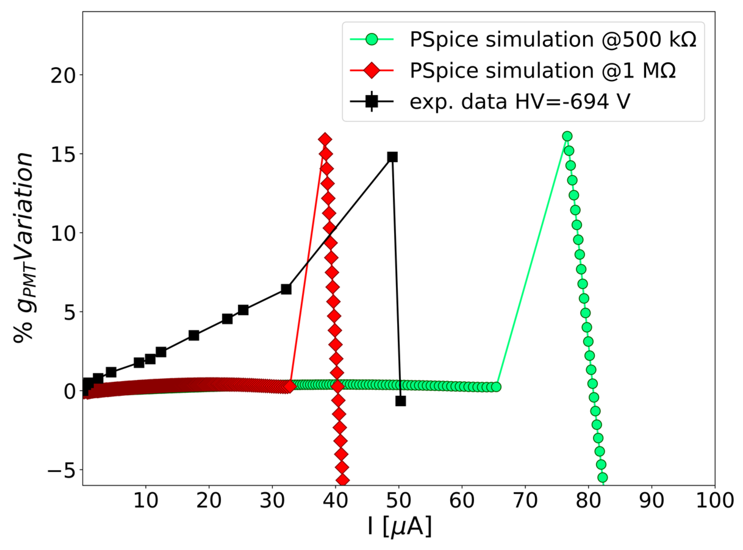
4.2. Simulation of the Circuit and PMT Response

The OrCAD [39] simulation tool, which utilizes the PSpice model [40], was employed to simulate the performance of the detectors at high rates. In this simulation, the schematics of the resistor network of the active base and the MOSFET stage, which provides bias to the R6231 Hamamatsu PMT dynodes, together with a model for the dynode stage amplification gain G D Y 8 = a ( Δ V ) k , were considered, where Δ V is the inter-dynode potential. The parameters a and k were adjusted, to reproduce the actual g versus V curve of the PMT used in the laser measurements, and are typical of this type of PMT (a = 0.19906; k = 0.72034). Furthermore, the collection efficiency Keff of the electrons produced by the dynode and moving toward the next dynode was considered. This efficiency is a function of the potential difference between the respective dynode and the following one, dV1. Keff tends to zero when the potential difference dV1 approaches zero; however, the exact behavior is not known. The PSpice model used in this work assumes a sigmoidal transfer function that results in a collection efficiency of 50%, with dV1 = 15 V. The sigmoidal function intervenes when the transistor cannot stabilize the voltage difference in the last dynode (i.e., above the breakdown) any more. At this point, the voltage difference decreases, and, when reaching 15 V, the sigmoidal function intervenes by lowering the output current of the last dynode. The relation between the collection efficiency Keff and dV1 used in the model is
K e f f = ( 1 + e ( d V 1 3 + 15 3 ) ) 1
It is worth noting that the collection efficiency does not affect the limiting current value but influences the gain variation percentage appearing after this value (as shown in Figure 14). For the simulation presented in this work, the collection efficiency was tuned to reproduce the experimental gain variation (at the energy of 1332 keV), as shown in Figure 14.
The solid line of Figure 11 was obtained with this procedure and reasonably describes the laser data. The solid line in Figure 13 represents the result of the simulations for the limiting rate as a function of gain and is also consistent with the data. The plot in Figure 14 shows the simulated gain variation as a function of the anode current. While the rise in gain within the operational range of the active base that was experimentally observed (and depending on the applied PMT voltage) is not well-reproduced by the simulation, the “breakdown” of the performance occurring at the limiting current is present. Its predicted dependence on the voltage divider values is confirmed, as illustrated by the green dashed line.

5. Discussion

The study of the conversion gain and linearity of the detector data shows that there is a variation in the gain with the count rate (and anode current) for both voltage divider types. Indeed, the effect is due to a combination of the charge per pulse and the pulse repetition rate. The detector with a resistor-type voltage divider has a larger variation with the count rate and exhibits a higher non-linearity in response to different energies. In contrast, the configuration with an active-type voltage divider demonstrates a more linear and stable response, making it the preferred choice for application in the G-NUMEN project.
The results obtained from the tests presented in this study establish a connection between the detector response, in terms of energy resolution and gain, and the changes in the anode current and in the supply voltage.
Figure 6 and Figure 7 allow for the extraction of the minimum gain at which the energy resolution requirements are met. A conversion gain of about 0.35 pC/keV should be sufficient to provide a good resolution at all energies. This gain value corresponds to an HV in the range of 750–850 V, depending on the detector. However, a limitation of the anode current in the active base is observed. Above a certain current value IL, the detector performance is degraded. The restriction on the anode current also translates to a limitation on the counting rate, at which the detector can effectively operate. In Section 4.1, it is demonstrated that such a limit, RL, can be estimated from Equation 5 by taking into account the HV and the voltage divider’s total resistance (RVD = 13 MΩ), and the maximum achievable counting rate for a detector operating with a good energy resolution is around 200 kHz. Reducing the voltage divider’s total resistance could help in achieving the desired count rate; however, other alternative designs of the active base are under consideration to also achieve better linearity and stability for the response.

6. Conclusions

This works presents the first tests of a prototype of the G-NUMEN array, performed under conditions similar to those foreseen for the NUMEN experiment. The results demonstrate that the detector performance is strongly influenced by the count rate as well as by the bias voltage and by the electronic configuration of the voltage divider. The findings of this work indicate that an active-type voltage divider could offer the best front-end electronics configuration for the detector array. However, limitations are observed in the anode current, with performance degradation occurring after reaching a specific value that depends on the voltage applied to the PMT. The limit in the anode current translates into a restriction on the count rate that is sustainable by the detector. While operating the PMT at lower voltages could potentially allow for higher count rates, this approach would compromise the energy resolution, which is a crucial requirement for the NUMEN project.
The calculations presented in this study provide valuable insights into determining the optimal electronic configuration for the future G-NUMEN array. This study demonstrates that in order to address the challenges encountered at detection rates comparable to those expected in the NUMEN project, improvements to the detector performance can be achieved by specifically modifying the active voltage divider’s circuit. These findings contribute to a better understanding of the detector’s behavior and offer guidance for optimizing its performance under various operational conditions.

Author Contributions

Conceptualization, E.M.G., L.C., J.R.B.O. and P.F.; methodology, J.R.B.O., D.P. and P.F.; validation, E.M.G., L.C., J.R.B.O. and P.F.; formal analysis, E.M.G., J.R.B.O., D.P., A.B. and D.T.; investigation, E.M.G., J.R.B.O., L.C., D.C. (Diana Carbone), D.C. (Daniela Calvo), D.P., A.B., M.C., I.C., F.D., C.E., F.L., N.M., M.M., V.R.S., D.S., A.S. and P.F.; resources, C.A., F.C., P.F. and F.D.; data curation, E.M.G.; writing—original draft preparation, E.M.G. and J.R.B.O.; writing—review and editing, F.D., D.P., A.B., D.C. (Diana Carbone) and P.F.; visualization, E.M.G. and P.F.; supervision, L.C., J.R.B.O. and P.F.; project administration, C.A. and F.C.; funding acquisition, C.A. and F.C. All authors have read and agreed to the published version of the manuscript.

Funding

This research was funded by INFN and by the Brazilian funding agencies FAPESP (protocol no. 2019/07767-1), CNPq (protocol no. 316019/2021-6), and INCT-FNA (protocol no. 464898/2014-5).

Data Availability Statement

The data presented in this study can be made available on request from the corresponding author.

Acknowledgments

The authors wish to thank the radiation protection staff of the LNS facility, as well as the technical staff of the ALTO facility, for their precious support and contribution to this work.

Conflicts of Interest

The authors declare no conflict of interest.

References

  1. Engel, J.; Menéndez, J. Status and future of nuclear matrix elements for neutrinoless double-beta decay: A review. Rep. Prog. Phys. 2016, 80, 046301. [Google Scholar] [CrossRef] [PubMed]
  2. Cappuzzello, F.; Agodi, C.; Bondì, M.; Carbone, D.; Cavallaro, M.; Foti, A. The role of nuclear reactions in the problem of 0νββ decay and the NUMEN project at INFN-LNS. J. Phys. Conf. Ser. 2014, 630, 012018. [Google Scholar] [CrossRef]
  3. Agodi, C.; Cappuzzello, F.; Bonanno, D.L.; Bongiovanni, D.G.; Branchina, V.; Calabretta, L.; Calanna, A.; Carbone, D.; Cavallaro, M.; Colonna, M.; et al. NUMEN Project @ LNS: Heavy ions double charge exchange reactions towards the 0νββ nuclear matrix element determination. In AIP Conference Proceedings, Proceedings of the Workshop on Calculation of Double-Beta-Decay Matrix Elements (MEDEX’15), Prague, Czech Republic, 9–12 June 2015; AIP Publishing: Melville, NY, USA, 2015; Volume 1686, p. 020001. [Google Scholar] [CrossRef]
  4. Cappuzzello, F.; Acosta, L.; Agodi, C.; Boztosun, I.; Brischetto, G.A.; Calabrese, S.; Calabretta, L.; Calvo, D.; Campajola, L.; Capirossi, V.; et al. The NUMEN Project: An Update of the Facility Toward the Future Experimental Campaigns. Front. Astron. Space Sci. 2021, 8, 668587. [Google Scholar] [CrossRef]
  5. Cappuzzello, F.; Agodi, C.; Calabretta, L.; Calvo, D.; Carbone, D.; Cavallaro, M.; Colonna, M.; Finocchiaro, P.; Iazzi, F.; Linares, R.; et al. The NUMEN Technical Design Report. Int. J. Mod. Phys. A 2021, 36, 2130018. [Google Scholar] [CrossRef]
  6. Cappuzzello, F.; Agodi, C.; Cavallaro, M.; Carbone, D.; Tudisco, S.; Presti, D.L.; Oliveira, J.R.B.; Finocchiaro, P.; Colonna, M.; Rifuggiato, D.; et al. The NUMEN project: NUclear Matrix Elements for Neutrinoless double beta decay. Eur. Phys. J. A 2018, 54, 72. [Google Scholar] [CrossRef]
  7. Cappuzzello, F.; Lenske, H.; Cavallaro, M.; Agodi, C.; Auerbach, N.; Bellone, J.; Bijker, R.; Burrello, S.; Calabrese, S.; Carbone, D.; et al. Shedding light on nuclear aspects of neutrinoless double beta decay by heavy-ion double charge exchange reactions. Prog. Part. Nucl. Phys. 2023, 128, 103999. [Google Scholar] [CrossRef]
  8. Carbone, D.; Ferreira, J.L.; Calabrese, S.; Cappuzzello, F.; Cavallaro, M.; Hacisalihoglu, A.; Lenske, H.; Lubian, J.; Vsevolodovna, R.I.M.; Santopinto, E.; et al. Analysis of two-nucleon transfer reactions in the 20Ne + 116Cd system at 306 MeV. Phys. Rev. C 2020, 102, 044606. [Google Scholar] [CrossRef]
  9. Ferreira, J.L.; Carbone, D.; Cavallaro, M.; Deshmukh, N.N.; Agodi, C.; Brischetto, G.A.; Calabrese, S.; Cappuzzello, F.; Cardozo, E.N.; Ciraldo, I.; et al. Analysis of two-proton transfer in the 40Ca(18O,20Ne)38Ar reaction at 270 MeV incident energy. Phys. Rev. C 2021, 103, 054604. [Google Scholar] [CrossRef]
  10. Sgouros, O.; Cavallaro, M.; Cappuzzello, F.; Carbone, D.; Agodi, C.; Gargano, A.; De Gregorio, G.; Altana, C.; Brischetto, G.A.; Burrello, S.; et al. One-proton transfer reaction for the 18O + 48Ti system at 275 MeV. Phys. Rev. C 2021, 104, 034617. [Google Scholar] [CrossRef]
  11. Cavallaro, M.; Bellone, J.I.; Calabrese, S.; Agodi, C.; Burrello, S.; Cappuzzello, F.; Carbone, D.; Colonna, M.; Deshmukh, N.; Lenske, H.; et al. A Constrained Analysis of the 40Ca(18O,18F)40K Direct Charge Exchange Reaction Mechanism at 275 MeV. Front. Astron. Space Sci. 2021, 8, 659815. [Google Scholar] [CrossRef]
  12. Burrello, S.; Calabrese, S.; Cappuzzello, F.; Carbone, D.; Cavallaro, M.; Colonna, M.; Lay, J.A.; Lenske, H.; Agodi, C.; Ferreira, J.L.; et al. Multichannel experimental and theoretical constraints for the 116Cd(20Ne,20F)116In charge exchange reaction at 306 MeV. Phys. Rev. C 2022, 105, 024616. [Google Scholar] [CrossRef]
  13. Spatafora, A.; Cappuzzello, F.; Carbone, D.; Cavallaro, M.; Lay, J.A.; Acosta, L.; Agodi, C.; Bonanno, D.; Bongiovanni, D.; Boztosun, I.; et al. 20Ne + 76Ge elastic and inelastic scattering at 306 MeV. Phys. Rev. C 2019, 100, 034620. [Google Scholar] [CrossRef]
  14. Carbone, D.; Carbone, D.; Linares, R.; Linares, R.; Amador-Valenzuela, P.; Amador-Valenzuela, P.; Calabrese, S.; Calabrese, S.; Cappuzzello, F.; Cappuzzello, F.; et al. Initial State Interaction for the 20Ne + 130Te and 18O + 116Sn Systems at 15.3 AMeV from Elastic and Inelastic Scattering Measurements. Universe 2021, 7, 58. [Google Scholar] [CrossRef]
  15. La Fauci, L.; Spatafora, A.; Cappuzzello, F.; Agodi, C.; Carbone, D.; Cavallaro, M.; Lubian, J.; Acosta, L.; Amador-Valenzuela, P.; Borello-Lewin, T.; et al. 18O+76Se elastic and inelastic scattering at 275 MeV. Phys. Rev. C 2021, 104, 054610. [Google Scholar] [CrossRef]
  16. Soukeras, V.; Cappuzzello, F.; Carbone, D.; Cavallaro, M.; Agodi, C.; Acosta, L.; Boztosun, I.; Brischetto, G.; Calabrese, S.; Calvo, D.; et al. Measurement of the double charge exchange reaction for the 20Ne + 130Te system at 306 MeV. Results Phys. 2021, 28, 104691. [Google Scholar] [CrossRef]
  17. Finocchiaro, P.; Acosta, L.; Agodi, C.; Altana, C.; Amador-Valenzuela, P.; Boztosun, I.; Brasolin, S.; Brischetto, G.A.; Brunasso, O.; Calabrese, S.; et al. The NUMEN Heavy Ion Multidetector for a Complementary Approach to the Neutrinoless Double Beta Decay. Universe 2020, 6, 129. [Google Scholar] [CrossRef]
  18. Cappuzzello, F.; Agodi, C.; Carbone, D.; Cavallaro, M. The MAGNEX spectrometer: Results and perspectives. Eur. Phys. J. A 2016, 52, 167. [Google Scholar] [CrossRef]
  19. Cavallaro, M.; Cappuzzello, F.; Carbone, D.; Cunsolo, A.; Foti, A.; Khouaja, A.; Rodrigues, M.R.D.; Winfield, J.S.; Bondì, M. The low-pressure focal plane detector of the MAGNEX spectrometer. Eur. Phys. J. A 2012, 48, 59. [Google Scholar] [CrossRef]
  20. Torresi, D.; Sgouros, O.; Soukeras, V.; Cavallaro, M.; Cappuzzello, F.; Carbone, D.; Agodi, C.; Brischetto, G.; Calabrese, S.; Ciraldo, I.; et al. An upgraded focal plane detector for the MAGNEX spectrometer. Nucl. Instrum. Methods Phys. Res. Sect. A Accel. Spectrometers Detect. Assoc. Equip. 2021, 989, 164918. [Google Scholar] [CrossRef]
  21. Oliveira, J.R.B.; Finocchiaro, P.; Agodi, C.; Boztosun, I.; Cappuzzello, F.; de Faria, P.N.; Gasques, L.; Linares, R.; Medina, N.H.; Mendes, D.R.; et al. New spectrometer projects for challenging particle-gamma measurements of nuclear reactions. J. Phys. Conf. Ser. 2017, 1056, 012040. [Google Scholar] [CrossRef]
  22. Oliveira, J.R.B.; for the NUMEN collaboration; Moralles, M.; Flechas, D.; Carbone, D.; Cavallaro, M.; Torresi, D.; Acosta, L.; Agodi, C.; Amador-Valenzuela, P. First comparison of GEANT4 hadrontherapy physics model with experimental data for a NUMEN project reaction case. Eur. Phys. J. A 2020, 56, 1–9. [Google Scholar] [CrossRef]
  23. Calabrese, S.; Cappuzzello, F.; Carbone, D.; Cavallaro, M.; Agodi, C.; Torresi, D.; Acosta, L.; Bonanno, D.; Bongiovanni, D.; Borello-Lewin, T.; et al. Analysis of the background on cross section measurements with the MAGNEX spectrometer: The (20Ne, 20O) Double Charge Exchange case. Nucl. Instrum. Methods Phys. Res. Sect. A Accel. Spectrometers Detect. Assoc. Equip. 2020, 980, 164500. [Google Scholar] [CrossRef]
  24. Gosta, G.; Blasi, N.; Camera, F.; Million, B.; Giaz, A.; Wieland, O.; Rossi, F.; Utsunomiya, H.; Ari-Izumi, T.; Takenaka, D.; et al. Response function and linearity for high energy γ-rays in large volume LaBr3:Ce detectors. Nucl. Instrum. Methods Phys. Res. Sect. A Accel. Spectrometers Detect. Assoc. Equip. 2018, 879, 92–100. [Google Scholar] [CrossRef]
  25. Nicolini, R.; Camera, F.; Blasi, N.; Brambilla, S.; Bassini, R.; Boiano, C.; Bracco, A.; Crespi, F.; Wieland, O.; Benzoni, G.; et al. Investigation of the properties of a 1″×1″ LaBr3:Ce scintillator. Nucl. Instrum. Methods Phys. Res. Sect. A Accel. Spectrometers Detect. Assoc. Equip. 2007, 582, 554–561. [Google Scholar] [CrossRef]
  26. Lavagno, A.; Gervino, G.; Scarfone, A. Study of linearity and internal background for LaBr3(Ce) gamma-ray scintillation detector. Nucl. Instrum. Methods Phys. Res. Sect. A Accel. Spectrometers Detect. Assoc. Equip. 2013, 718, 504–505. [Google Scholar] [CrossRef]
  27. Aldawood, S.; Castelhano, I.; Gernhäuser, R.; Van Der Kolff, H.; Lang, C.; Liprandi, S.; Lutter, R.; Maier, L.; Marinšek, T.; Schaart, D.R.; et al. Comparative Characterization Study of a LaBr3(Ce) Scintillation Crystal in Two Surface Wrapping Scenarios: Absorptive and Reflective. Front. Oncol. 2015, 5, 270. [Google Scholar] [CrossRef]
  28. Quarati, F.; Khodyuk, I.; van Eijk, C.; Quarati, P.; Dorenbos, P. Study of 138La radioactive decays using LaBr3 scintillators. Nucl. Instrum. Methods Phys. Res. Sect. A Accel. Spectrometers Detect. Assoc. Equip. 2012, 683, 46–52. [Google Scholar] [CrossRef]
  29. Quarati, F.; Owens, A.; Dorenbos, P.; de Haas, J.; Benzoni, G.; Blasi, N.; Boiano, C.; Brambilla, S.; Camera, F.; Alba, R.; et al. High energy gamma-ray spectroscopy with LaBr3 scintillation detectors. Nucl. Instrum. Methods Phys. Res. Sect. A Accel. Spectrometers Detect. Assoc. Equip. 2011, 629, 157–169. [Google Scholar] [CrossRef]
  30. Löher, B.; Savran, D.; Fiori, E.; Miklavec, M.; Pietralla, N.; Vencelj, M. High count rate gamma-ray spectroscopy with LaBr3:Ce scintillation detectors. Nucl. Instrum. Methods Phys. Res. Sect. A Accel. Spectrometers Detect. Assoc. Equip. 2012, 686, 1–6. [Google Scholar] [CrossRef]
  31. Kerns, C.R. A High-Rate Phototube Base. IEEE Trans. Nucl. Sci. 1977, 24, 353–355. [Google Scholar] [CrossRef]
  32. Hiebert, R.; Thiessen, H.; Obst, A. Photomultiplier tube base for high pulsed anode currents. Nucl. Instrum. Methods 1977, 142, 467–469. [Google Scholar] [CrossRef]
  33. Heifets, M.; Margulis, P. Fully active voltage divider for PMT photo-detector. In Proceedings of the 2012 IEEE Nuclear Science Symposium and Medical Imaging Conference Record (NSS/MIC), Anaheim, CA, USA, 27 October–3 November 2012; pp. 807–814. [Google Scholar] [CrossRef]
  34. Popov, V.; Mkrtchyan, H. New photomultiplier active base for Hall C jefferson lab lead tungstate calorimeter. In Proceedings of the 2012 IEEE Nuclear Science Symposium and Medical Imaging Conference Record (NSS/MIC), Anaheim, CA, USA, 27 October–3 November 2012; pp. 1177–1179. [Google Scholar] [CrossRef]
  35. Ren, P.-P.; Lin, W.-P.; Wada, R.; Liu, X.-Q.; Huang, M.-R.; Tian, G.-Y.; Luo, F.; Sun, Q.; Chen, Z.-Q.; Xiao, G.-Q.; et al. An active base designed in high-counting-rate applications for Hamamatsu R1924A photomultiplier tube. Nucl. Sci. Tech. 2017, 28, 145. [Google Scholar] [CrossRef]
  36. Wang, B.; Chen, L.; Liu, Y.; Yin, W.; He, Z.; Jin, G. Design of a High-Count-Rate Photomultiplier Base Board on PGNAA Application. In Proceedings of International Conference on Technology and Instrumentation in Particle Physics 2017; Springer Proceedings in Physics; Springer: Singapore, 2018; Volume 212, pp. 142–146. [Google Scholar] [CrossRef]
  37. CAEN Digitizer VX2745 and Firmware. Available online: https://www.caen.it/products/vx2745/ (accessed on 1 August 2023).
  38. Hamamatsu Photonics, K.K. Photomultiplier Tubes—Basics and Applications, 3rd ed.; Hamamatsu Photonics K.K.: Fukuoka, Japan, 2006. [Google Scholar]
  39. OrCAD Simulation Tool. Available online: https://www.orcad.com/ (accessed on 1 August 2023).
  40. PSpice Model. Available online: https://www.pspice.com/ (accessed on 1 August 2023).
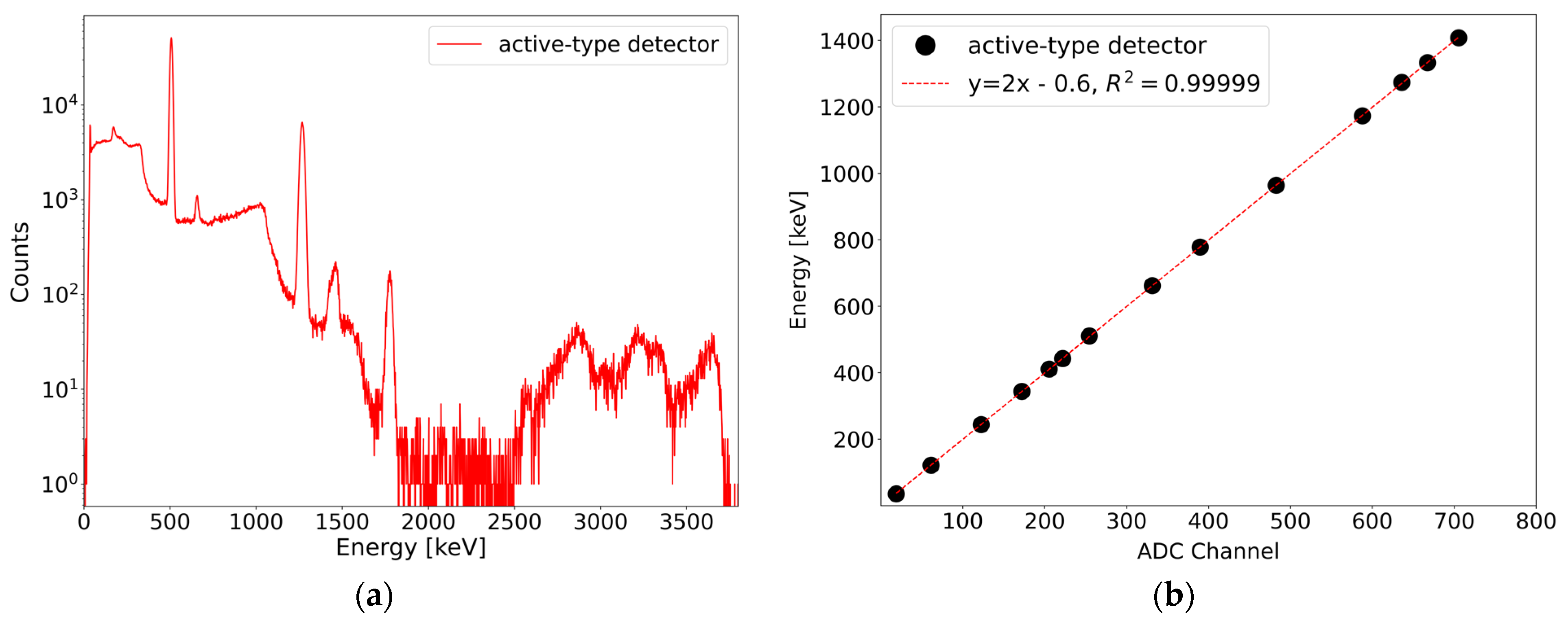
Figure 1. Design of the G-NUMEN array. (a) LaBr3(Ce) detectors are placed around the scattering chamber, supported by individual mechanical shells. (b) The scattering chamber (in yellow) gives a constraint for the minimum distance possible (24 cm) between target and scintillators and for the maximum solid angle coverage.
Instruments 07 00028 g001
Figure 2. (a) Typical spectrum obtained with one of the LaBr3(Ce) detectors exposed to a 22Na source that produces gamma rays of 511 and 1275 keV. The voltage bias was −1000 V. (b) The channel-to-energy linear calibration plot. The energy peaks used for the calibration are listed in Table 1. The error bars are the same size as the data point symbols.
Instruments 07 00028 g002
Figure 3. (a) The prototype of one shell of the G-NUMEN array. (b) The typical background spectrum of the scintillators to be used in the NUMEN experiment. In the spectrum, it is possible to notice the low energy peaks from the ε-decay of 138Ba, related to the cascade products originated by the electron capture in the K and L atomic shells; a β-continuum spectrum related to the 138La that decays into 138Ce, in which the 789 keV gamma peak escaped the detector, and the end point is 255 keV; a Compton continuum spectrum in the region 255–750 keV due to the contribution of both 789 keV and 1436 keV; a photopeak at 789 keV from the 138Ce decay, widened due to the β spectrum emitted in coincidence, which results in a continuum region with an endpoint around 1 MeV; a photopeak at 1436 keV from the 138Ba decay, which is detected in coincidence with the K and L cascade, resulting in a wider peak around 1472 keV; a high-energy part of the spectrum related to the contamination of 227Ac, producing alpha particles with an energy of gamma-ray equivalence in the range of 1.8–3.3 MeV.
Instruments 07 00028 g003
Figure 4. (a) Characterization in energy resolution (FWHM (%)) of the detectors at low counting rates in the two configurations with resistor-type (black) and active-type (red) voltage dividers using 22Na, 60Co,137Cs, and 152Eu, calibration sources, and the self-activity peaks. (b) The measured intrinsic photopeak efficiency is in agreement with literature data [24,25]. If not visible, the error bars are smaller than the data point symbols.
Instruments 07 00028 g004
Figure 5. (a) Relative variation in the gain with the detection rate (i.e., average anode current) for the scintillator with resistor-type (gray) and active-type (orange) voltage dividers. The different data points represent the energy peak of the 137Cs (square), the intrinsic activity peak at 1472 keV (circle), and the last peak of the intrinsic activity related to the ɑ contamination of the crystal (triangle). (b) Differential gain ratio as a function of integral gain for different detectors at low rates (see text). The PMT supply voltage for all active-type detectors was −937.5 V. Each data point corresponds to a different active-type detector.
Instruments 07 00028 g005
Figure 6. (a) Differential gain (using the 1332 keV gamma peak) of two active-type detectors as a function of the supply voltage. The solid lines are fits to the data using Equation (2). (b) Energy resolution (FWHM (%)) of the 1332 keV peak as a function of the gain (varied by application of different PMT voltages) for the same two active-type detectors that show very different PMT gains at the same voltage. The error bars are smaller than the data point symbols.
Instruments 07 00028 g006
Figure 7. Energy resolution (FWHM (%)) as a function of gain for various gamma-ray energy lines. The error bars are smaller than the data point symbols.
Instruments 07 00028 g007
Figure 8. (a) Variation in the gain with the detection rate at different energies for resistor-type (black and blue) and active-type (red) voltage dividers. The blue point shows the response of the detector for rate up to 310 kHz, obtained with a fusion–evaporation reaction. The black and red points refer to the test performed with an intense 137Cs source, for which the maximum detection rate achieved was 180 kHz. (b) Gain at the 662 keV peak as a function of the anode current for two active-type detectors at different voltages. If not visible, the error bars are smaller than the data point symbols.
Instruments 07 00028 g008
Figure 9. Sample detector signals before (green) and after (red) reaching the limiting current.
Instruments 07 00028 g009
Figure 10. Details of the experimental setup for the laser measurement. The optical fiber is installed sideways with respect to the LaBr3(Ce) crystal. The laser light is sent through the optical fiber directly to the window of the PMT.
Instruments 07 00028 g010
Figure 11. Limiting current versus applied voltage for 4 different detectors (magenta triangles: laser data; squares, circles, and yellow triangles: gamma data for three other detectors). Blue solid line with diamonds: PSpice simulations for the laser data. Light blue dashed line: voltage divider current of the active base divided by two (IVD/2, see text). If not visible, the error bars are smaller than the data point symbols.
Instruments 07 00028 g011
Figure 12. Simplified schematics of the active base, highlighting the active stage for stabilization of the last dynode (DY8) potential (V8).
Instruments 07 00028 g012
Figure 13. Experimental data (squares and circles), simple model prediction (red dashed line), and PSpice simulations for the laser data (blue solid line with diamonds) of the limiting rate, as a function of the gain. The orange dotted line is the model prediction, by halving the total resistance value of the active-type voltage divider. The gray dotted line indicates the conversion gain (g = 0.35 pC/keV) sufficient to obtain a good energy resolution in the case of the NUMEN experiment (see Section 5). If not visible, the error bars are smaller than the data point symbols.
Instruments 07 00028 g013
Figure 14. Conversion gain variation (%) as a function of the anode current at −694 V. Black squares: data points obtained with gamma-ray measurements using the 1332 keV peak of the 60Co source and employing the 430 keV laser pulse for tuning the anode current. Red solid line and diamonds: simulated gain with value of the currently employed voltage divider resistors (1 MΩ). Green dashed line and circles: simulation with halving of the voltage divider resistors’ values.
Instruments 07 00028 g014
Table 1. Data used for the channel-to-energy linear calibration of Figure 2.
Energy (keV)ChannelNote
35.51935.5 keV gamma peak from internal radioactivity of LaBr3(Ce)
12261152Eu gamma peak
244122152Eu gamma peak
344177152Eu gamma peak
411205152Eu gamma peak
443222152Eu gamma peak
511255annihilation of 22Na positron
662331137Cs gamma peak
778390152Eu gamma peak
964483152Eu gamma peak
117358860Co gamma peak
127563522Na main gamma peak
133266760Co gamma peak
1408705152Eu gamma peak
Disclaimer/Publisher’s Note: The statements, opinions and data contained in all publications are solely those of the individual author(s) and contributor(s) and not of MDPI and/or the editor(s). MDPI and/or the editor(s) disclaim responsibility for any injury to people or property resulting from any ideas, methods, instructions or products referred to in the content.

