1. Introduction
Rectifiers are a primary tool for delivering power from the electric grid to the local consumer by converting AC to DC voltage. Most switch–mode power converter topologies can be utilized as a single–phase power–factor correction (PFC) rectifier [
1]. The basic idea is to impose a pure resistance input impedance at the rectifier input terminal. Thus, the rectifier is required to operate continuously to keep a near unity power factor and eliminate all harmonics. This principle of operation is valid for single–phase or three–phase rectifiers [
2]. For this purpose, the boost converter is the most widespread rectifier; However, it imposes a minimum DC bus voltage of ~375 V (to preserve continuous operation at the maximum amplitude of the sine wave). Most residential and commercial loads are electronic circuitry that consumes DC power. However, the grid supplies pulsating power; therefore, an additional energy storage element is required to supply continuous power. The electrolytic capacitor is commonly used as a PFC output terminal energy storage element. This element is responsible for about thirty percent of PFC failures [
3] due to excessive heat dissipation and high operating–voltage ripple. Nevertheless, this issue could be addressed by implementing an electronic capacitor [
4]. The boost rectifier [
1] is a highly efficient, low–cost, and relatively simple PFC stage with relatively high voltage output. Nonetheless, a typical DC load consumes energy under a certain (much lower) voltage supply and consequently requires an additional conversion stage. As a result, the cost, volume, weight, and efficiency are negatively affected.
The conventional boost rectifier presents significant conduction losses because the current always flows through the switching devices. The converter should operate at high switching frequencies to achieve high power density and faster transient response. Nevertheless, the diode reverse–recovery losses become significant as the switching frequency rises and the electromagnetic interference increases. A bridgeless topology has been presented in [
5] to overcome the conduction losses. The diode reverse–recovery problems are alleviated using only a coupled inductor and two additional diodes. As the rectifier power level increased, a parallel interleaved bridgeless boost converter [
5] was employed to improve the performance and reduce the size. In such an operation, the active ripple frequency is twice the switching frequency or more; thus, the input and output ripples are minimized, and the output capacitance and the input filter sizes can be drastically reduced. In the half–bridge boost converter, the current flows through one switch during each operating stage, drastically reducing conduction losses. In this topology, the output voltage is doubled while keeping the component stress voltage at the same level as a standard converter.
The buck is a step–down converter that may solve the necessity for lower voltage applications. In this topology, the output voltage must be lower than the input source voltage. Thus, the buck rectifier cannot sustain continuous operation throughout the grid cycle [
1]; the input current is discontinued when the instantaneous line voltage is lower than the output voltage. Therefore, it cannot maintain the required power factor and total harmonic distortion. Buck–type PFC rectifiers allow a more comprehensive control range for the output rectified voltage (corresponding to the boost–type topologies) [
6]. Due to the operation’s nature, the output–voltage regulation depends on the load impedance; therefore, a larger output filter is compulsory. A bridgeless buck topology has an improved performance over the standard buck converter as a high–power levels PFC converter [
5]. It offers the same current flow with a reduced number of switching devices, hence reducing thermal stress. Moreover, it introduces a higher efficiency operation with reduced input current THD, cutting down the conduction losses and ensuring that the output voltage on the DC bus is naturally balanced. The interleaved buck topology [
7] has advantages like the interleaved boost–type topology. The bridgeless interleaved topology is highly efficient (95–97%) from light to full–load at universal input voltage [
8].
By contrast, the buck–boost rectifier is much more versatile since it supports a voltage step–up and step–down; consequently, a wide output–voltage range is available. Nevertheless, a buck–boost rectifier is relatively less efficient; the reversing output voltage can cause a conflict with the neutral point, and the inductor peak current is higher than in a similar power boost rectifier [
1]. The bridgeless buck–boost topology is based on two basics single–switch buck–boost converters, each operating over a half–grid cycle [
9]. It offers high power–quality performances with low THD
i and near unity power factor under a wide load range. The structure of bridgeless buck–boost topologies is complex and limited to low–power applications [
10]. The bridgeless cascaded buck–boost topology presents a reduced number of conducted switches. It escalates the electromagnetic interference and increases the voltage sensing complexity, while the efficiency is higher than the standard topology (95–97%) at a wide load range and near unity power factor [
11].
The penetration of stochastic renewable sources into the electrical grid [
12] requires energy backup support utilized by storage systems. Batteries are among the most appropriate storage technologies due to their energy density, volumetric density, fast response time, availability, and installation simplicity near the power generation plant and at the distribution consumption location [
13]. The energy storage charging process is controlled by power electronics circuitry; in the grid–connected applications, a near unity power factor within limits of total harmonic distortion standard is mandatory. This requires a significant amount of energy to be stored in a series cell structure, which creates a high–voltage battery. As in electric vehicles (EVs), the battery voltage can swing above and below the standard rectified voltage; thus, a wide output–voltage range is required.
The Vienna rectifier introduced an innovative approach for three–phase rectifiers. Compared with a conventional two–level converter system, the three–level Vienna rectifier reduces the voltage stress on its switches and the rated power of inductance connected on the side of the mains. The three–level DC bus is more applicable for inverters since the three–level inverter enables higher efficiencies and better harmonics immunity compared with two–level inverters [
14]. However, the Vienna rectifier’s output voltage is twice as high as a standard boost PFC rectifier with bus voltages of ~–400 V, neutral (0 V), and ~+400 V. This rectifier type may fit applications such as low harmonics three–level inverters and high–voltage, high–power motor drives. Applications with low–power motors, such as air–conditioners, refrigerators, etc., may require lower amplitude sine waves, where the high–voltage three–level DC bus reduces the resolution; therefore, the accuracy of the inverter may also harm the inverter’s efficiency. In such a case, an additional conversion step is the preferred option for decreasing the DC bus voltage. The emergence of fully EVs and hybrid plug–in vehicles brought new challenges for power electronics engineers and pushed the battery energy density limits to new levels; although optimization of battery size was made [
15], the battery capacity remains over tens of kilo watts hours, and requires powerful, fast chargers [
16] or powerful wireless chargers [
17]. The nominal charging voltage in EV applications varies between 100 V and 1000 V [
18]. Thus, the available rectifiers cannot support universal charging in a single conversion step. A comprehensive output–voltage range [
19] could be achieved by utilizing an additional conversion step; however, the overall efficiency is negatively affected. Moreover, the system cost, volume, weight, and component failure rate increase when employing two–stage conversion. The contribution of this paper compared to [
20,
21] is as follows. Unlike [
20,
21], where the rectifier runs in open–loop mode, a dual–loop controller (for the inductor current and output voltage) is implemented here:
Experimental results are given in this paper ([
20,
21] has only simulation); it was shown that some of the results reported in [
20,
21] are unachievable because of practical driving limitations.
Elaboration on the optional utilization of the bi–directional switch and the analysis of the required control command for each case.
The average current mode control method for discontinuous–conduction mode (DCM) operation is implemented here.
This paper presents a new topology for a single–step universal three–level PFC rectifier (UTPR) operating in dual–loop mode. The output–voltage range can swing between 50 V and 900 V while keeping the UTPR elements at half the size of a standard buck–boost rectifier. Unlike standard buck–boost, the UTPR creates three output–voltage levels that directly fit three–level inverters for improved voltage total harmonic distortion (THD
V). The UTPR employs fewer components than a standard dual–step converter. Therefore, the UTPR overall efficiency is higher, and the component count is lower than in a similar traditional system. The UTPR is relevant to applications such as EVs [
22], battery storage systems [
12], inverters [
23] or multi–level inverters [
24], and front–end rectifiers [
25]. First, the principles of operation and circuit analytics are introduced. Then, the UTPR average model and control approach is presented. Next, the UTPR circuit (operating in DCM) simulation and experimental results are provided, demonstrating the proposed circuit performance in a multiplier–less dual loop and validating the proposed theory of the innovative topology. Then, the results and outcome are discussed, and the conclusion is provided.
2. Circuit Topology and Analysis
In the meaning of the broad input and output–voltage range of a three–level PFC rectifier, the UTPR can fulfill all required properties. The proposed rectifier can operate in a single phase for light to medium loads or as a three–phase topology for high–power loads. The single–phase UTPR is based on one power inductor (
L), two storage capacitors (
C), and three bi–directional switches (
SW), as presented in
Figure 1. The UTPR can operate in continuous–conduction mode (CCM) [
26] and DCM [
27].
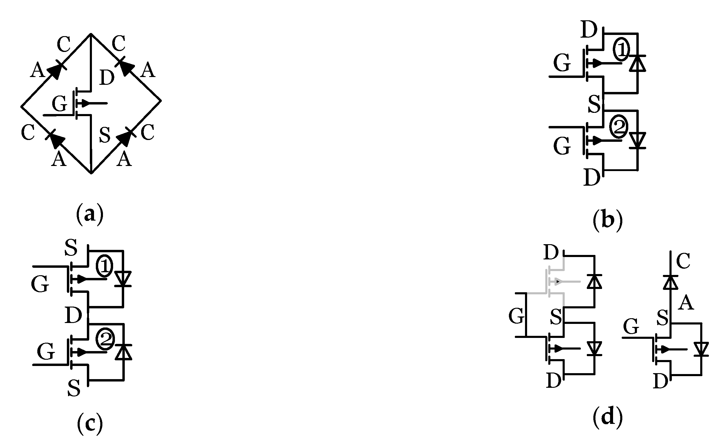
Several methods could be employed for a bi–directional
SW. The most straightforward technique for AC–connected
SWs is by four diodes and a single transistor (MOSFET, GaN FET, SiC, or IGBT). The diodes are connected in a rectifying fashion where the transistor drain is attached to the common cathode and the source to the common anode, as exhibited in
Figure 2a. Another option is a series connection of two transistors with a common source or drain connection, as presented in
Figure 2b and
Figure 2c, respectively. In many applications, the switching timing sequence is crucial; consequently, particular logic circuitry or high computational switching effort is required. A possible solution is a semi–open bidirectional
SW, where the opposing flow transistor is turned on before the inductor current is “looking” for a possible path; the second transistor anti–parallel diode blocks the unwanted flow. Next, when the inductor voltage reverses, the diode polarity turns ON and conducts (the
SW is ON now). To reduce the losses, the active diode transistor can be turned ON. The same results could be achieved by a semi–open
SW, where a drain of the transistor is series connected with the diode anode, as given in
Figure 2d. The drawback of this switch is the unidirectional current flow; thus, its utilization is limited to specific cases.
The principle of operation for the positive half–sine wave includes a charging period and a discharging interval of the power inductor. The charge path (marked in
Figure 3 as (a)) begins at the AC source throughout the main
SW (
Q1 at the middle), goes to the power inductor, and goes back to the neutral, as presented in
Figure 3a. The discharge path (marked as (b)) at the positive half–sine wave continues with the same current direction, discharging the inductor throughout the upper capacitor and the top
SW (
Q2). In the discharge period, the upper capacitor is charged within the current flow direction, as marked in
Figure 3b. The logic signals for driving the
SWs are as follows: the main
SW (
Q1) is governed by the PWM signal, and the upper SW (
Q2) is ruled by the complementary PWM signal with the condition of operating in the sine positive half–wave
.
In the negative half–sine wave, the charge path (marked in
Figure 4 as (a)) begins at the neutral and goes through the power inductor, to the main
SW (
Q1), and back to the AC source, as exhibited in
Figure 4a. The discharge path (marked in
Figure 4 as (b)) continues in the same direction as the current flow, discharging the inductor’s stored energy through the bottom capacitor and the lower
SW (
Q3). The bottom capacitor is charged within the current flow direction, as marked in
Figure 4b. The logic signals for driving the
SWs are as follows: the PWM signal governs the main
SW (
Q1), the bottom
SW (
Q3) is controlled by the complementary PWM signal with the condition of operating in the sine negative half–wave
.
The analysis of UTPR is made for two operation modes, the CCM and the DCM. In CCM, the UTPR output voltage is in three–level mode, and the converter voltage gain is
where
is the input terminal connected to the electrical grid r.m.s voltage (
), the
is the load voltage (where
), and the
is the rectifier’s duty cycle for
r.m.s values. The inductor’s current ripple is derived from the inductor voltage balance equation and from Equation (1), where the current ripple is
where
L is the inductance of the power inductor, and
is the switching frequency. Thus, the average inductor current is
where
is the load average current (
). Therefore, the inductor peak current is
and the minimum inductor for CCM is
where
Is the inductor value of critical mode, and
is the average output load power. As for DCM, since the UTPR shares similar characteristics as the buck–boost converter, the input average current exhibits a perfect linear relationship with its input voltage given by
where
is the inductor’s duty cycle for the conduction interval when operating at DCM for the
r.m.s values. From power equality and Equation (6), the converter transfer function is revealed in Equation (7), where the DCM duty cycle (
) can be revealed.
In standard rectifiers, under the assumption of unity power factor, the output capacitor value is set by the following rules of power equality, where
is the instantaneous input power, and
is the instantaneous capacitor power:
The capacitor energy balance is derived from Equation (8)
From Equation (9), the capacitor value is revealed as
where
is the rectifier output filter capacitor and
is the capacitor voltage ripple. Nevertheless, the UTPR operating principle resembles a single–phase Vienna rectifier [
26]. Each capacitor on UTPR is charged only in a one–half cycle and supplies energy for a whole period, as presented in
Figure 3 and
Figure 4. Both capacitors must contain a hold–up energy for a half–cycle time to fulfill the energy requirements, as shown in Equation (11).
where
is the capacitor hold–up time. Thus, an increased output capacitance is mandatory to support the required output–voltage ripple when employing a three–level rectifier. Applying a proportional integral and notch voltage controller decreases output capacitance, as presented in [
28]. The output capacitor is set by the maximum value of Equations (10) and (11)
It is easy to obtain that the hold–up capacitor is more significant than the ripple capacitor ; hence, the output capacitors are set by the value. Since a half–cycle energy hold–up time is a standardization requirement for every grid–connected system at a specific power rating, the capacity of UTPR is equal to any other rectifier topology. In the case of a three–phase rectifier, the low–frequency power signals are shifted at 120°, and the summation of all three voltage components is near zero ripple; hence, the required output capacitance is much lower than in a single phase.
3. Average Model and Control Approach
A cascade dual–control loop [
29] is a standard methodology to tackle converter stabilization tasks [
30]. An internal loop to shape the inductor current for PFC properties creates a sinusoidal envelope shape and an external outer voltage loop for the rectifier output–voltage adjustment, as presented in
Figure 5. The rectifier output voltage contains a slight sinusoidal fluctuation at double–line frequency; therefore, the controller output command (
iref) is a DC signal. However, the required current shape in the line frequency is sinusoidal; thus, an analog multiplier is necessary, as presented in
Figure 5.
Where
d* is the reference command for the duty cycle. The converter state equations present a non–linear system that is uncontrollable. The standard method to tackle this issue is modeling the converter’s continuous form as an average model. It is important to note that this model describes each half–sine wave separately; however, since the overall circuit activity is the same, both circuits are presented as a single model in
Figure 6. On the input side, the input voltage is marked as
vS, the
rS reflects the output active load multiplied by the operating–point duty ratio divided by the square of the output–to–input voltage–transfer function, and the last element is the average input current (
) multiply by the operating–point duty ratio. The output side is affected by the input voltage multiplied by the output–to–input voltage–transfer function divided by the output active load, and the next element is the average input current multiplied by the operating–point duty ratio; the other elements are the state operating capacitor (
CX) according to the positive or negative sequence, and the output active load. A small signal state equation is accomplished by applying Kirchhoff’s voltages and currents laws on the UPTR average model and splitting the parameters into intermediate components and perturbations. The state equations can be constructed by applying Kirchhoff’s voltages and currents laws on the UPTR average model and separating the parameters into average components and perturbations.
When operating the UTPR in DCM, the input current is a function of the input voltage and other parameters; thus, a near–unity PF is achieved naturally. Since the switching frequency has been higher than the line frequency for several decades, the line voltage is assumed to be almost constant in a single switching cycle. Under the steady–state operation assumption, the output voltage, and the duty ratio variation are slight. By performing an analysis on the UTPR, the line average current and the voltage present a perfect linear relationship, which proves that the UTPR has excellent self–PFC properties, as given in Equation (13) [
31]. Consequently, the UTPR control schematics do not necessitate a multiplier, simplifying the control effort (analog or digital) and reducing the control circuitry cost.
The state equations can be constructed by applying Kirchhoff’s voltages and currents laws on the UTPR. However, these state equations produce an uncontrollable non–linear system (with common compensators). The standard method to tackle this issue is transferring the converter’s continuous form using an average model. Separating the average model parameters into DC components, intermediate (first–order) components, and perturbations (second–order) yields the inductor state equation, as shown in Equation (14). The plant is dismantled into coefficients utilized for system input parameters. The functional block diagram includes the transfer function of the inductor current to the duty–cycle input signal (
Gid), where the input–voltage vector is set to zero.
where the
Is and the
Io are the rms input and output current, respectively,
Vs is the rms input voltage,
L is the inductor value,
Ts is the switching cycle period,
d1 is the duty cycle (ON time),
C is the capacitor value, and
R is the load resistance (ohmic). The UTPR output–voltage state equation is revealed in Equation (15). It is important to note that the output of the voltage controller is not multiplied by the absolute value of the sinusoidal waveform as in the standard rectifiers.
The state equation includes the UTPR output–voltage transfer function to the inductor current reference input signal (
Gvc), where the input–voltage vector is set to zero, and the input state vector coefficient (
Gvs), where the input reference voltage vector is set to zero. Unlike a standard rectifier, the control scheme does not require a multiplier, as presented in
Figure 7, where the
Gcv(
s) is the voltage loop compensator and the
Gci(
s) is the current loop compensator.
4. Simulation and Experimental Results
Based on the above analysis, the proposed UTPR circuit parameters were designed for multiplier–less dual–loop conditions at DCM. A DELL OPTIPLEX 7060 PC made the simulation with the PSIM tool (PSIM Professional 2022.2.0.17) operating at a switching frequency of
. The input voltage was set to
. In the design of the UTPR power inductor, the circuit output load was put into two conversion modes: step–up and step–down. At buck operation, the output load was set to 430 ohms (
) and the output load voltage to 75 volts (
). At the boost mode, the output load was set to 4000 ohms (
Ω) and the output load voltage to 400 volts (
). By employing Equation (5), the minimal critical inductance was found to be
; thus, the actual inductance was determined to be
. The output ripple voltage was set to
; according to Equation (12), the output capacitors were set to
(each) to satisfy the required output ripple voltage and the hold–up demand. Applying Equation (7), the duty ratio is revealed where
for the buck mode and
for the boost mode. The current control loop bandwidth was set to one decade below the switching frequency (10 kHz) and the voltage to one decade below the line frequency (5 Hz). The controllers’ coefficients were determined by assuming a nominal input voltage of 230 V, an output capacitor voltage of 275 V, and a load of 2.2 kilo ohm. The integration coefficient was found to be
ki = 314.5. Under the assumption of a damping coefficient in a near–critical point with a value of 0.8, the proportional coefficient value is
kp = 0.83. The voltage loop PI controller integration coefficient is
ki = 112.6, and with a dumping constant of 0.8, the proportional coefficient is
kp = 0.066. Based on the above analysis, the proposed UTPR prototype parameters were designed for operation at DCM with the same values as in the simulation. The switching frequency was set to
, a resistive load of
. The revealed inductor from Equation (5) is
, and by Equation (14), the output capacitor was set to
. The circuit was fed by the California Instruments 751i AC Power Supply. The Texas Instruments C2000 Delfino MCU F28379D LaunchPad™ governed the UTPR. The MCU measured the line voltage and synchronized all required logic signals to drive the UTPR switches. The UTPR main
SW Q1 was utilized by the combination of Transphorm 950 V/15 A TP90H180PS GaN FET and the supporting four blocking Schottky diodes of ONSEMI 1.2 kV/10 A, the FFSP10120A in fashion as in
Figure 2a. The upper switch
Q2 and lower switch
Q3 were utilized with the same devices in style shown in
Figure 2d, as given in
Table 1. The UTPR experimental board is presented in
Figure 8.
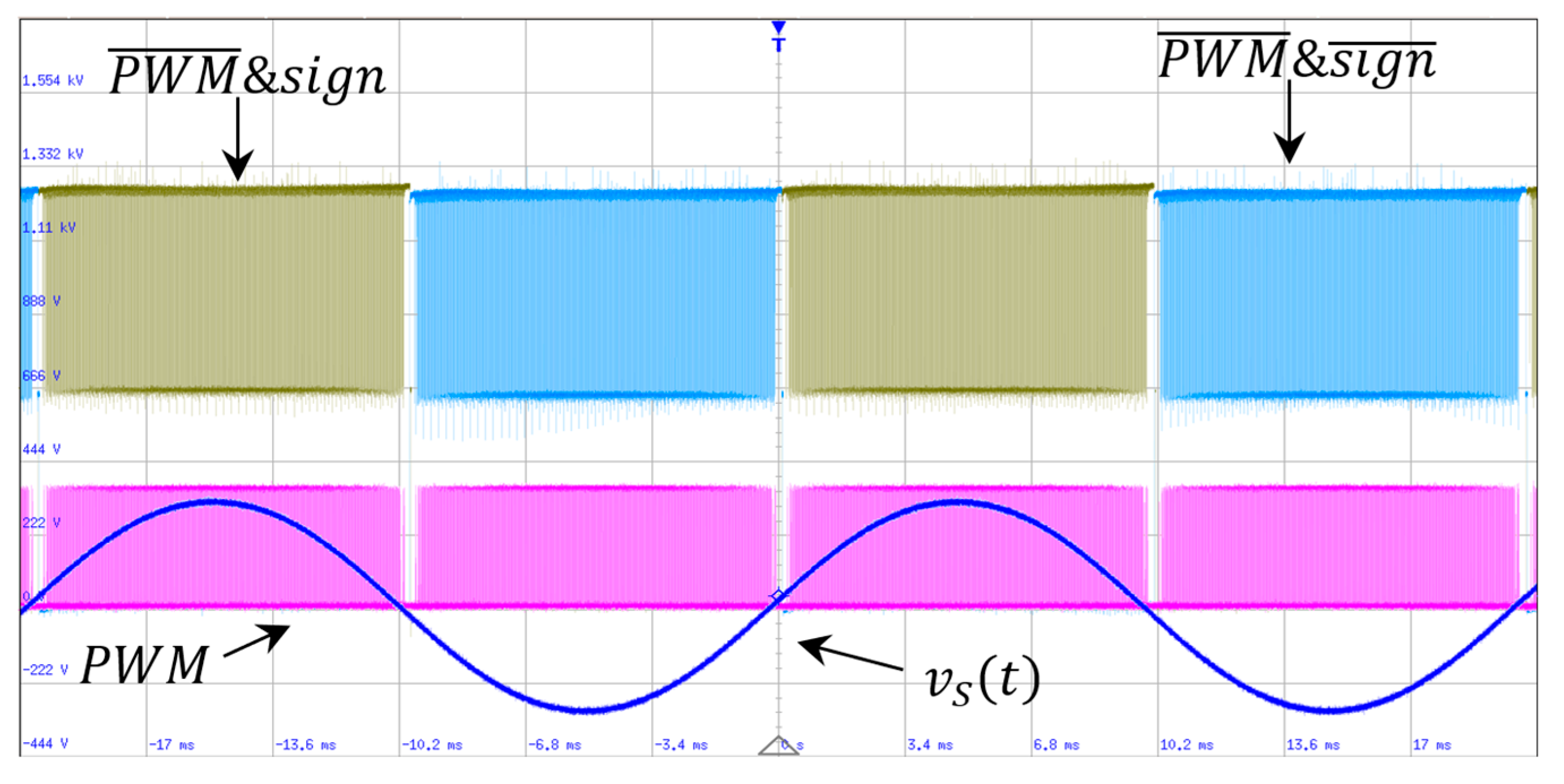
The UTPR was designed for DCM operation when its control system operates in a multiplier–less dual loop; the reference signal was set according to Equation (7). Measurements were carried out with a 200 MHz Rohde & Schwarz RTM3000 oscilloscope equipped with a power analysis tool. The command signals for the switches were set as mentioned above; the main switch (
Q1) receives the
signal, the upper switch (
Q2) is active during the positive line cycle and, therefore, receives the
, and the lower switch (
Q3) is active at the negative line sequence and acquire
. The command signals for all switches are presented in
Figure 9.
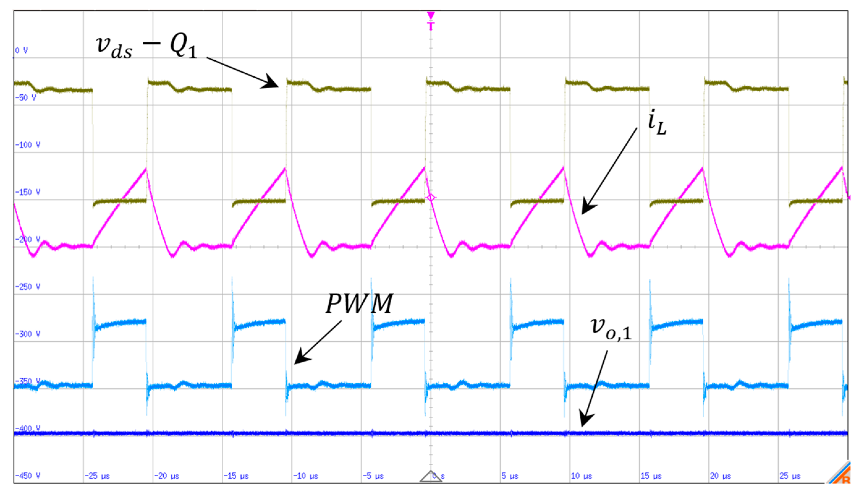
The UTPR principle of operation is similar to that of all switch–mode power supplies, where the inductor is charged during ON time. It delivers the accumulated energy to the output capacitor and the load during the discharge time, as explicit in
Figure 10. The specific frame was taken during the positive line sequence where the inductor current is positive, and the output capacitor voltage is negative concerning the line neutral.
In the boost mode, experimental results display an input voltage of
, an output capacitor voltage of
, and a load voltage of
, as shown in
Figure 11a. In buck mode, under the same grid supply voltage, the output voltage was
, and the load voltage was
. In both cases, the inductor current envelope allows the input–voltage shape, as shown in
Figure 11b. The power factor is near unity (
), as indicated in
Figure 11c. Although the UTPR runs at a multiplier–less dual loop, the inductor current shape is sinusoidal, an inherent feature of the buck–boost converter.
5. Discussion
The simulation and experimental results show that when operating in DCM, the UTPR can operate at a wide range in boost and buck modes. Although the control loop does not contain a multiplier, the rectifier input current envelope is aligned with the input–voltage phase, presenting a self–PFC. The results acknowledge the validity of the proposed theory, the developed analytics, and the UTPR average model. When comparing the proposed rectifier to a standard dual–stage rectifier, the component count for this topology for a single phase is one inductor, two capacitors, three MOSFETs, six diodes, and one dual–loop controller. A standard dual–stage rectifier has two inductors, two capacitors, two MOSFETs, six diodes, and two dual–loop controllers. The UTPR employs one more switch, one less power inductor, and one less dual–loop controller than a standard dual–stage rectifier. The efficiency of UPTR is expected to be higher than that of a standard dual–stage rectifier since it utilizes a single conversion step.
Bidirectional SW has multiple implementation methods; each topology’s component count, conduction losses, and static losses differ. The main
SW (
Q1—connected to the source
) could be implemented by the
SWs from
Figure 2a,
Figure 2b, or
Figure 2c (but not by
Figure 2d). The static and dynamic losses and the control instructions for each case are presented in
Table 2. The upper and lower
SWs (
Q2 and
Q3, respectively) are suitable for use by all
SWs, as shown in
Figure 2. The static and dynamic losses, alongside the control instructions for each case, are presented in
Table 2.
One of the drawbacks of the UTPR operating in a single phase is the high–value output capacitance. As in the Vienna rectifier, each output capacitor is not charged during one–half of the line cycle. Moreover, since the inductor in the UTPR is not constantly connected to the input or the output, the peak current is higher than in step–down rectifiers. Future work on the subject will be implementing the dual–loop controller for DCM and CCM at a single–phase rectifier and then into a three–phase interleaved rectifier where the circuit dynamics will be analyzed. When implementing a three–phase rectifier, the output capacitance could be minimized to near zero. A parallel interleaving approach is sufficient to decrease the inductor peak current.

 ,
, 


