1. Introduction
Recently, the X-ray photoelectron spectroscopy (XPS) method has been extensively used in modern material science, becoming the most frequently employed not only in the fundamental research of surface sciences and nanomaterials, but also in applied multidisciplinary areas of chemistry [
1], biology [
2,
3], medicine [
4,
5], etc. The considerable interest of researchers in the XPS method is due to the possibility of obtaining information not only about the composition of the surface of solids, but also about its chemical state, which allows to improve synthesis recipes and develop new materials with desired functional properties. The combination of laboratory XPS analysis and synchrotron techniques allows us to solve a variety of questions in material science. In particular, the use of angle resolved XPS and photoelectron spectroscopy based on synchrotron sources with tunable photon energy in tandem allows to determine the distribution of elements in the surface and near-surface layers of multi-component structures with high accuracy [
6,
7,
8].
The method of XPS is based on the photoelectric effect, a phenomenon in which X-rays are absorbed by the substance and an electron (photoelectron) is emitted into the vacuum, for which its energy is analyzed. This effect is described by the extended Einstein equation for the photoelectric effect and has the following form
hν =
KE +
BEj +
φ, where
KE is the kinetic energy of the photoelectron,
BEj is the electron binding energy at the j-electron level in the atom, and
φ is the work function. The desired value in the equation is the binding energy—
BEj, while the kinetic energy of the photoelectron is determined experimentally. The binding energy of a photoelectron is a characteristic value for each electronic shell of an element of the substance; therefore, the XPS method makes it possible to perform a qualitative analysis of a solid. As a rule, the simplest task of XPS is reduced to recording spectra and comparing characteristic photoemission lines with existing databases, for example, with the most common NIST [
9]. According to a review conducted by G. Greczynski and L. Haltman which considers the number of scientific articles in the Scopus database related to the XPS method, the number of published works is significantly increasing every year [
10]. Among the authors of the research papers, there is a tendency to compare the experimental data with the data presented in published articles. This approach is quite justified since with technological progress, the accuracy of modern laboratory instruments increases, which makes it possible to achieve a better spectral resolution, comparable to the unique synchrotron Megascience class facilities. However, the growing popularity and availability of XPS unfortunately inevitably leads to a decrease both in the quality of results and their interpretation, which can lead to dramatic consequences in terms of the reproducibility of scientific results [
11,
12]. For correct interpretation of XPS data, researchers have to thoroughly understand the process of the interaction of ionizing radiation with matter, as well as to possess knowledge in the field of quantum chemistry, but often insufficient time is devoted to studying the basics of XPS, which leads to inadequate experiment planning. In the case of multicomponent material analysis, where the photoelectronic signal of the primary structure of the spectrum (core and Auger electron lines) may overlap with the signal of the secondary structure (spin–orbit and multiple splitting, satellites and plasmons, etc.), the complexity of interpreting XPS data is greatly increased, and even in some cases, not possible at all. Careful experiment planning can help to not face such scenarios, in particular, to avoid overlapping of the photoelectron lines of the core and Auger electrons. In some cases, it is sufficient to select the appropriate energy of the exciting X-ray source, at which the Auger electron transition is impossible or shifted from the core photoelectron lines [
13,
14,
15,
16,
17].
In recent years, the number of publications on XPS studies of nitrogen-doped carbon nanotubes (N-CNTs) has been rapidly increasing due to high prospects for the use of N-CNTs for energy conversion and storage [
18,
19,
20,
21,
22]. The electrical properties and catalytic activity of N-CNTs significantly depend on the concentration of doping nitrogen and its distribution according to the incorporation type in the N-CNT structure between pyrrole-, graphite-, and pyridine-like nitrogen [
23,
24,
25,
26,
27]. The method of XPS makes it possible to characterize with high accuracy the type of chemical bonds of doping nitrogen with carbon and to establish the dependence of the N-CNT properties on the type of nitrogen incorporation. Thus, pyridine-like nitrogen has been shown to increase the surface wetting and catalytic activity of N-CNTs to develop efficient catalysts and supercapacitors [
28,
29,
30]. The pyrrole-like nitrogen introduces significant distortions into the nanotube structure due to the formation of five-atom rings and leads to the formation of bamboo-like defects [
31,
32]. Bamboo-like defects, in turn, can lead to the formation of anomalous piezoelectric properties in N-CNTs to develop nanogenerators [
33,
34,
35]. In this case, the material of the lower electrode, on which the N-CNTs are grown, significantly affects the concentration of doping nitrogen and its distribution according to the incorporation type [
36]. The maximum concentration of doping nitrogen is observed in N-CNTs grown on a Mo electrode [
36]. This fact is due to the lowest interaction between the nitrogen precursor and Mo during the nanotube growth and the preferential incorporation of nitrogen into the nanotube structure rather than the lower electrode. However, difficulties arise due to the overlapping of N1s and Mo3p
3/2 photoelectron core lines during XPS analysis of the N-CNTs on a Mo electrode.
In this paper, using the XPS technique, we analyze a multicomponent system based on nitrogen doped multi-walled carbon nanotubes grown on a Mo substrate. We demonstrate step by step the process of interpreting data using laboratory and synchrotron X-ray radiation sources by precise deconvolution of overlapping N1s and Mo3p3/2 photoelectron core lines. From the point of view of the rationality of using synchrotron accelerator complexes, we carried out a comparative analysis of the results obtained from the study of a laboratory spectrometer and a synchrotron source. The results presented in our paper allow us to plan the experiment in detail at the stage of choosing between laboratory and accelerator instruments for the XPS method.
2. Materials and Methods
Experimental samples of N-CNTs were grown by plasma-enhanced chemical vapor deposition (PECVD) in acetylene and ammonia flows. The process gas flow ratio of acetylene and ammonia was 70 and 210 cm3/min, respectively. The temperature of the samples’ growth was 645 °C. The p-Si (100) was used as substrate on the surface of which a Mo lower electrode film of 100 nm thick and a Ni catalytic layer film were deposited by magnetron sputtering using an AUTO 500 (BOC Edwards, Crawley, UK). The thickness of the nickel catalytic layer was 5 nm and 15 nm for S1 and S2 samples, respectively. The power of used plasma is 40 W. The growth time was 15 min.
As is known, the process of the N-CNT growth by the PECVD method consists of four stages: sample heating, activation of catalytic centers, growth of N-CNTs, and sample cooling. At the stage of heating, a mixture of argon gas with a flow of 40 cm
3/min and ammonia with a flow of 15 cm
3/min is supplied to the PECVD chamber. The pressure in the chamber is maintained at a level of 4.5 Torr. At this stage, fragmentation of the initial film of the catalytic layer occurs with the formation of catalytic centers; the geometric dimensions, density, and chemical composition of which affect the parameters of the grown N-CNTs. At the activation stage, the formed catalytic centers are subjected to additional holding in the ammonia flow (210 cm
3/min) at a given temperature. As a result, partial or complete reduction of the catalytic center metal occurs. During the growth stage, acetylene and ammonia are supplied to the reaction chamber. At this stage, an important task is to take into account the interaction of acetylene and ammonia flows with a Mo lower electrode, since the formation of molybdenum nitrides and carbides affects the concentration of free carbon and nitrogen atoms on the catalytic center surface. The ratio of carbon and nitrogen concentrations is responsible for the degree of concentration and type of forming defects (pyridine-, graphite-, and pyrrole-like) in the substitution of carbon by nitrogen [
31,
33].
The characterization of geometric parameters and structure of the experimental samples was carried out by scanning electron microscopy (SEM) using Nova NanoLab 600 (FEI, Eindhoven, The Netherlands) in secondary electrons mode and by transmission electron microscopy (TEM) using Tecnai Osiris (FEI, Eindhoven, The Netherlands). The X-ray photoelectron spectroscopy measurements were carried out in ultrahigh vacuum (UHV) 10–10 mbar conditions using commercial K-Alpha Themo Scientific spectrometer (ThermoScientific, Waltham, MA, USA) with monochromatic Al Kα (1486.6 eV) X-ray source and using synchrotron X-ray radiation source (850 eV) at the RGBL Dipole beamline of BESSY II Light Source—Helmholtz-Zentrum Berlin (HZB, Berlin, Germany) [
37]. The survey spectra recorded in the binding energy region of −10–750 eV and the pass energy (PE) was set at 200 eV for Al Kα X-ray source and 70 eV for the synchrotron radiation source, respectively. High-resolution spectra were recorded in fixed analyzer transmission (FAT) mode with PE = 30 eV. Energy scale calibration was performed by position of maxima Au 4f
7/2 high-resolution spectra collected from a standard gold sample with 99.99% purity. We determined the exact photon energy value and subsequently determined the position of the spectra relative to the Fermi level, taking into account that the binding energy of the Au 4f
7/2 photoelectrons of bulk gold is 84 eV.
High-resolution spectra data were collected with energy step size of 0.1 eV and number of scans
n = 10 for Al Kα source and 0.025 eV, 3 scans for synchrotron radiation source, respectively. For quantification, Shirley and Tougaard background functions and relative sensitivity factors (RSF) from Scofield libraries were chosen [
38]. During the component analysis, the best shape of the fitted curves was achieved with a Lorentz/Gauss function mixture at the ratio of 40/60.
The piezoelectric response of the N-CNTs was studied using the method of force spectroscopy of atomic force microscopy (AFM) at the Ntegra probe nanolaboratory (NT-MDT, Moscow, Russia). The piezoelectric response is a current flow between the grounded AFM probe and the strained N-CNT having surface potential during its deformation. The force value applied to the AFM probe increased from 0 to 2 µN. The AFM probe was a silicon probe with a conductive TiN coating and a curvature radius at 35 nm.
3. Results and Discussion
Figure 1a,b shows SEM images of the N-CNT S1 and S2 samples. As can be seen, the density of N-CNTs in the array for the S1 sample is lower than for the S2 sample, while the geometric parameters of nanotubes are closed (
Table 1). The aspect ratio of the nanotube length L to the diameter D is about 17 and 20 for samples S1 and S2, respectively. The survey XPS (
Figure 1c,d) spectra show the main elemental composition of the sample surface, which includes carbon, oxygen, molybdenum, and nitrogen. The characteristic difference in the survey spectra obtained from different sources is the presence of oxygen O
KLL Auger electron transitions in the 337 eV region when using the 850 eV synchrotron radiation source (SRS) (
Figure 1d). According to the principles of XPS and Auger electron spectroscopy, a change in the energy of the excitation source leads to a shift in the photoemission lines on the kinetic energy scale. The kinetic energy values of Auger electrons are an unchanged characteristic of the electronic structure, and is a fingerprint for each atom [
39]. In the XPS method, we calculate the binding energies of core electrons, which do not depend on the energy of the excitation photon. Therefore, the Auger electron lines are shifted by an amount equal to the difference in excitation photon energies between the synchrotron and laboratory radiation sources (LRS) when converting to a binding energy scale:
Thus, the O
KLL line with the SRS is shifted on the binding energy scale relative to the O
KLL (973.3 eV) with the laboratory Al Kα (1486.6 eV) source by −636.6 eV and takes a value of 336.7 eV. Similarly, there is a signal from the carbon C
KLL Auger electron line at 583 eV on the survey spectrum of the S2 sample (
Figure 2d). In addition, the difference is also seen in the presence of peaks at 103.5 and 154.4 eV, which correspond to the photoemission lines of silicon bound to oxygen SiO
2 (Si2p and Si2s, respectively) [
9]. We assume that the presence of a photoelectronic signal from silicon in the case of the S2 sample is due to the imperfection of the Mo electrode in the form of a local rupture of the interface with the surface of the silicon substrate. This fact may be due to the larger thickness of the catalytic layer and the denser array of N-CNTs (
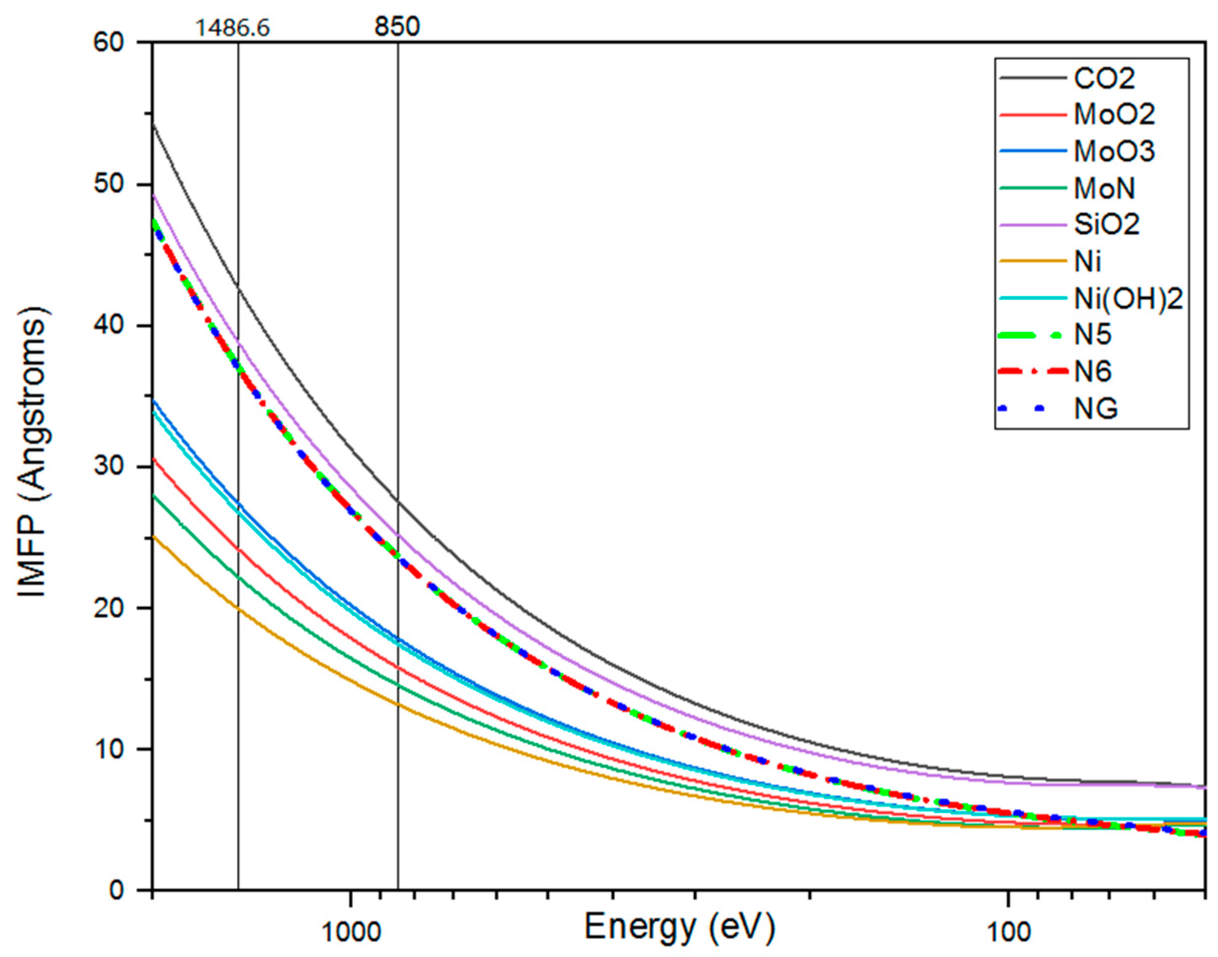
Figure 1b). This statement is supported by the fact that the analyzed depth in the SRS case is smaller than in the LRS. We estimated the depth of the analyzed layers by calculating the inelastic mean free path of electrons using the S. Tanuma, C. J. Powell, D. R. Penn (TPP-IMFP) algorithm [
40].
Figure 2 shows the curves of TPP-IMFP dependence on photon energy for the compounds pyrrole-like (N5), piridine-like (N6), graphite-like nitrogen (NG), MoO
2, MoO
3, MoN, SiO
2, Ni, and Ni(OH)
2.
Table 2 presents the values for their calculation.
We excluded the interaction of silicon with the N-CNTs by analyzing the spectra of photoelectron lines C1s (
Figure 3a blue curve) and Si2p (
Figure 1f). The shapes and positions of the curves indicate the absence of Si-C bonds, which for the silicon line correspond to Si2p3 ~100.3 eV and for the carbon line C1s ~283 eV [
9]. Furthermore, the temperature for silicon carbide formation (over 1500 °C) is much higher than nanotube growth (645 °C). This fact also excludes the formation of silicon carbide. The comprehensive analysis of N-CNTs using XPS and TEM methods allowed us to establish that a nickel catalyst in the form of nanoparticles diffuses into the nanotubes during N-CNT growth. This fact is confirmed by the weak Ni2p signal obtained from the AlKa source. Moreover, we did not detect a nickel photoelectron signal in the synchrotron experiments due to the fact that the depth of the analyzed layer in the SRS with the excitation source at 850 eV is slightly lower than in the LRS with Al Kα (1486.6 eV). This also indicates the diffusion of nickel particles into N-CNTs. Analysis of the presented high-resolution nickel Ni2p3 spectrum (with LRS at Al Kα 1486.6 eV) (
Figure 1e) indicates that the nickel particle has the form of a metallic nanocluster covered with hydroxide with characteristic components of Ni + 2 (855.7 eV) and Ni + 0 (853 eV) [
41]. The poor photoelectron signal of Ni2p3 does not allow for a component analysis to accurately determine the amount of nickel hydroxide.
In our calculations, we take into account the contribution of the photoelectron signal from silicon to the surface composition of N-CNTs by excluding the integral signal of the oxygen fraction that accounts for it. However, the concentration dependencies in
Table 1 do not take into account the fraction of the signal that corresponds to the overlapping photoelectron lines of N1s and Mo3p
3/2. The S1 sample calculation of the element atom concentrations is carried out by determining the curve areas of the corresponding components and their normalization as follows:
where
Nelement—x-element concentration;
Snorm—normalized area under the peak of the x-element;
Fx—sensitivity factor of the x-element, which depends on the orbital;
Tx—transmission function (depends on the sensitivity factor);
Cx—attenuation length, correction for the free path length of non-elastically scattered electrons. The values
Fx,
Tx, and
Cx are defined from the Scofield libraries. Quantification of the element atom concentrations for the synchrotron measurements of the S2 sample is carried out using J.J. Yeh and I. Lindau photoionization cross-section data [
42] as follows:
where
—integral intensity of the x spectral line,
—photoionization cross-section of x element spectral line, and
—photon flux.
As can be seen, the difference between the surface composition of the samples is the ratio of oxygen, nitrogen, and molybdenum. On the one hand, this is due to the morphology structure of the samples, where in the case of the S1 sample, the N-CNT density is lower, which indicates a larger signal from the Mo electrode; on the other hand, this is due to a calculation error related to the overlap of the N1s and Mo3p3/2 photoelectron lines.
To determine the composition of the surface in detail, it is necessary to use high-resolution spectra, which allows us to calculate more accurately the areas under the peaks.
Figure 3a–d shows the high-resolution spectra of C1s, O1s, N1s, and Mo3d for the S1 sample—red curves and the S2 sample—blue curves, respectively. As can be seen, the shape and position of the intensity maxima of the photoelectron lines differ from sample to sample, which indicates a different stoichiometric ratio. The main task here is to separate the photoelectronic signal related to the core electrons N1s and Mo3p
3/2.
For this purpose, we deconvoluted the high-resolution spectra of Mo3d and determined the component composition of molybdenum (
Figure 4a,b). According to the results of deconvolution, it was established that for both samples, molybdenum has a different degree of oxidation from Mo
1+ to Mo
6+, while its oxides and nitrides were found. According to the literature sources, the fitted components of the Mo3d photoemission line correspond to MoN, MoO
2, MoO
x, and MoO
3 (the position of the binding energies shown in
Table 3) [
43,
44,
45,
46].
Table 4 shows the components and the concentration ratios obtained from the results of deconvolution of the high-resolution spectra of Mo3d. It is known that when chemical bonds are formed, a change in the energy states of the outer orbitals also leads to a change in the inner ones. In this regard, the ratio of the components for the Mo3p
3/2 photoelectron lines should be proportional to the ratio of the Mo3d
5/2 components. Applying the obtained concentration ratios of the molybdenum components for the photoelectron overlapping core lines of N1s and Mo3p
3/2, we deconvoluted the spectra (
Figure 4c,d). The result of deconvoluting the high-resolution spectra of the overlapping of photoemission lines for N1s and Mo3p
3/2 indicates the presence of components corresponding to the compounds MoN, MoO
2, MoO
x, and MoO
3 (
Table 4), which agrees with the results obtained in
Figure 4a,b.
The analysis of the obtained results shows that the thickness of the nickel catalytic layer has a significant effect on the concentration of molybdenum nitride in Mo lower electrodes. Thus, the MoN concentration decreases from 13.48 to 2.17% with an increase in the thickness of the nickel catalytic layer from 5 to 15 nm (
Table 4). This dependence is due to different probabilities of the formation of molybdenum oxide MoO
x and bonding with the catalytic layer in the form of MoNi
3 during the formation of catalytic centers at the stage of sample heating. So, the reaction with the formation of MoNi
3 is more likely to proceed at a thickness of Ni at 5 nm, and the process of oxidation of molybdenum with the formation of MoO
x is more likely at a thickness of 15 nm. Further, during the growth of N-CNTs at the stages of activation and heating, the interaction of MoNi
3 with ammonia leads to the formation of molybdenum nitride, and the interaction of MoO
x with ammonia can gradually reduce the oxide to metallic molybdenum. In this case, the formation of molybdenum nitride leads to a redistribution of the ratio of the concentration of free carbon and nitrogen during the growth of N-CNTs. This fact leads to a redistribution of doped nitrogen between pyridine-, pyrrole-, and graphitic-like forms [
33,
35].
This statement is in agreement with the results of reconstructing the fine structure of the nitrogen line, which includes pyridine-, pyrrole-, and graphitic-like forms, pyridine oxide, and molybdenum nitride N-Mo (binding energies present in
Table 3), based on separation of the photoelectronic signal of photoemission lines for N1s and Mo3p
3/2. Component analysis allowed us to calculate the areas under the curves related to the N1s photoelectronic signal (
Table 5) and to obtain the refined values of the surface composition (
Table 6).
The proportion of pyrrole-like nitrogen is 27% and of pyridine-like is 15% of the total nitrogen content in the N-CNTs of the S1 sample (
Table 6). In the S2 sample, the concentration of pyrrole- and pyridine-like nitrogen increases to 35% and 20%, respectively. This dependence is due to the fact that the concentration of free nitrogen increases with a decrease in the formation of molybdenum nitrides, with an increase in the thickness of the nickel catalytic layer. As a result, the ratio of free nitrogen and carbon flows entering the surface of catalytic centers during the growth of N-CNTs increases. This fact leads to the predominant formation of pyrrole-like nitrogen [
33]. The concentration of pyrrole-like nitrogen, in turn, determines the piezoelectric properties of N-CNTs [
33,
34,
35].
The results of the AFM study of the samples showed an increase in the piezoelectric response of N-CNTs from 12 to 17 nA with an increase in pyrrole-like nitrogen from 1.77 to 2.05% (
Figure 5a). As we have previously found, the generation of current during the deformation of N-CNTs is due to the formation of a surface potential as a result of the manifestation of the piezoelectric properties of N-CNTs [
48]. The origin of the piezoelectric properties of N-CNTs are bamboo-like defects in the cavity of the nanotube (
Figure 5b), which are a curved graphene sheet with a non-zero dipole moment due to curvature-induced polarization [
49]. The total polarization of N-CNTs is the sum of the dipole moments of all bamboo-like defects per unit volume [
34]. As a result, it is necessary to increase the number of bamboo-like defects, which is determined by the concentration of pyrrole-type nitrogen, to increase the piezoelectric response of N-CNTs [
33]. Thus, the observed increase in the piezoelectric response for the S2 sample relative to the S1 sample is in agreement with the previously proposed mechanism of the piezoelectric effect in N-CNTs, which is associated with the formation of bamboo-like defects as a result of the incorporation of pyrrole-like nitrogen [
33].
Thus, it has been shown that deconvolution of the high-resolution spectra of overlapping photoemission lines for N1s and Mo3p
3/2 makes it possible to efficiently restore the fine structure of the nitrogen line and separate the components of pyridine-, pyrrole-, and graphitic-like nitrogen and molybdenum nitride, both in the laboratory and the synchrotron XPS method. The obtained results allowed us to study the effect of the thickness of the nickel catalytic layer of the N-CNT samples on the concentration and the type of doping nitrogen and piezoelectric response. At the same time, the calculation of the element atom concentrations of the N-CNTs by determining the curve areas of the corresponding components and their normalization gives overestimated values of nitrogen concentration due to overlapping core lines of N1s and Mo3p
3/2 (
Table 1).
In this way, the analysis of the high-resolution spectra and deconvolution results indicates that the interpretation of XPS results primarily depends on the sequence and algorithm used for calculating the fine structure. The overlapping N1s and Mo3p3/2 photoelectron core lines lead to significant difficulties in peak fitting, which requires the development of guides in the analysis of multicomponent systems of the N-CNTs/Mo type by the XPS method. The described process in this study of interpreting XPS data makes it possible to avoid gross errors in the study of the surface composition and nitrogen components of the N-CNTs. It is shown that a correct analysis of XPS spectra provides very important information about the distribution of nitrogen over emerging defect types, which later determine the chemical and electrical properties of the N-CNTs.


 ,
, 


