

Validation of Easy Fabrication Methods for PDMS-Based Microfluidic (Bio)Reactors

Chair for Bioprocess Engineering, Department of Biochemical and Chemical Engineering, TU Dortmund University, D-44227 Dortmund, Germany
*
Author to whom correspondence should be addressed.
Sci 2022, 4(4), 36; https://doi.org/10.3390/sci4040036
Submission received: 23 December 2021
/
Revised: 15 July 2022
/
Accepted: 15 September 2022
/
Published: 21 September 2022
(This article belongs to the Special Issue Feature Papers 2021 Editors Collection)
Abstract
:The common method for producing casting molds for the fabrication of polydimethylsiloxane (PDMS) chips is standard photolithography. This technique offers high resolution from hundreds of nanometers to a few micrometers. However, this mold fabrication method is costly, time-consuming, and might require clean room facilities. Additionally, there is a need for non-micromechanics experts, who do not have specialized equipment to easily and quickly prototype chips themselves. Simple, so-called, makerspace technologies are increasingly being explored as alternatives that have potential to enable anyone to fabricate microfluidic structures. We therefore tested simple fabrication methods for a PDMS-based microfluidic device. On the one hand, channels were replicated from capillaries and tape. On the other hand, different mold fabrication methods, namely laser cutting, fused layer 3D printing, stereolithographic 3D printing, and computer numerical control (CNC) milling, were validated in terms of machine accuracy and tightness. Most of these methods are already known, but the incorporation and retention of particles with sizes in the micrometer range have been less investigated. We therefore tested two different types of particles, which are actually common carriers for the immobilization of enzymes, so that the resulting reactor could ultimately be used as a microfluidic bioreactor. Furthermore, CNC milling provide the most reliable casting mold fabrication method. After some optimization steps with regard to manufacturing settings and post-processing polishing, the chips were tested for the retention of two different particle types (spherical and non-spherical particles). In this way, we successfully tested the obtained PDMS-based microfluidic chips for their potential applicability as (bio)reactors with enzyme immobilization carrier beads.
Keywords:
on-chip biotransformation; enzyme; biocatalysis; microfluidics; soft lithography; PDMS; 3D printing1. Introduction
In modern chemical, pharmaceutical, and food industries the application of biocatalysts has become more and more widespread [1,2]. Biocatalysts catalyze one or more steps in an enantio- and regioselective way, often surpassing chemical catalysts [3]. In biotechnology, an increasing number of alternatives to chemical catalysts as well as novel reactions are being researched. Since these reactions are often not the reactions that are naturally catalyzed by the enzymes, many enzyme variants and reaction conditions must be tested in a very short time [4]. Microfluidic devices enable the acceleration of such screenings by reducing the required reaction time and parallelization [5]. Microfluidic chips are a few centimeters in size, and traversed by thin, submillimeter channels. Fluids and gases are pumped through the chip, enabling controlled and highly-defined reaction conditions. The lab-on-a-chip concept for microfluidic devices offers the possibility to miniaturize an entire laboratory onto a chip [6], thereby enabling the rapid and cost-effective biotransformation and analysis of cells and enzymes [7,8]. These devices offer an opportunity to analyze biotransformations quickly and directly at the smallest scale, thereby reducing the required reaction components to a minimum. The chips are usually easy and cheap to fabricate and enable the parallelization of experiments for high-throughput screenings, for example, of different biocatalyst variants. When enzymes are analyzed, these are often immobilized so that they remain in the chip and are not flushed out by the continuous flow. The immobilization of the enzymes can be performed on the inner walls of the microreactors, in monolithic-type channels, or on the surface of the porous solid particles inside, resulting in a packed microreactor [9,10]. The latter is advantageous in terms of the amount of enzyme per reactor volume and is therefore often the preferred method. Particle trapping can be classified into contact-based and contactless methods, which can also be differentiated into methods that require external energy (contactless methods) and methods that do not require external energy (contact-based method) [11,12]. Contact-based methods turned out to be efficacious for many applications, thereby being simultaneously easy to fabricate. Hydrodynamic trapping methods are often used as mechanical barriers that sieve the particles and thereby immobilize them at specific locations [13].
For the fabrication of microfluidic chips, three different material classes are mainly used. These are inorganic materials such as glass or ceramics; polymers such as polydimethylsiloxane (PDMS), polyfluoropolyethers, poly(methylmethacrylate) (PMMA), polystyrene (PS), cyclic olefin copolymer (COC), and SU-8; and, lastly, paper [14,15]. Each material has advantages and disadvantages. Paper-based microfluidic devices offer great potential for inexpensive and portable medical diagnostic systems [16]. A negative aspect is their low durability. When high durability is required, glass microfluidic devices are the best choice [17]. However, materials and fabrication are expensive and therefore glass is not the recommended material for prototyping [18]. Polymers are cheap and suitable for easy and fast prototyping. PDMS was chosen for microfluidic chip fabrication in this study due to many benefits. It is biocompatible and gas permeable, thereby offering good conditions for enzyme reactions. The Sylgard 184 silicone elastomer (Dow Corning Corporation) used is supplied as a two-part liquid component kit. It consists of a pre-polymer base and a crosslinking curing agent. When both components are mixed, the PDMS polymerizes in the presence of platinum [19]. Curing takes place at room temperature and is quickened at elevated temperatures up to 200 °C [20]. This offers the potential to pour it over a casting mold and to replicate the mold’s structures precisely. Furthermore, PDMS is compatible with many solvents, which offers the opportunity to clean the PDMS-based microfluidic device after usage to extend its usability [21]. However, PDMS may swell and become brittle after some time. PDMS also offers low autofluorescence properties, which is essential for fluorescence analysis [22]. The cured PDMS is flexible and transparent (Figure 1).
The common method for producing molds for the fabrication of PDMS chips is standard photolithography. Photolithography offers high resolution and reproducibility [23]. However, this mold fabrication method requires specialized laboratories and equipment, such as clean room facilities, and is costly and time-consuming. Various alternative methods exist in general for casting mold fabrication, for example, 3D printing methods, such as fused deposition modeling, selective laser sintering, photo-polymer inkjet printing, and stereolithography [24,25]. The comparison of fused deposition modeling, selective laser sintering, photo-polymer inkjet printing, and stereolithography revealed that fused deposition modeling and selective laser sintering result in surfaces that are too rough, which lead to non-transparent PDMS replicas and poor bonding [24]. The roughness of 3D-printed replicas can additionally result in a gradual transition of the edges to the bonding area, which then leads to fluid stagnation close to the channel boundaries [26]. Using particles in such systems, they also stagnate in these areas and become permanently stuck. A post-treatment for the surface polishing prior to use as a casting mold was not tested.
In addition to the resins usually used for these manufacturing processes, some alternatives were developed with improved properties that are less toxic and avoid the evaporation of monomers [27,28]. The influence on replica quality has not been reported. Laser engraving-based methods have also been developed, which can be used to produce casting molds based on metal, polystyrene, or even tape [29,30,31]. However, these methods have not yet been tested for their application to the fabrication of a microfluidic packed-bed reactor in which immobilization carrier particles are mechanically retained. For these purposes, photolithographic fabrication methods are usually used, as they are considered to be precise and reliable [32,33,34].
The aim of this study was therefore to develop a microfluidic device with an easy and cheap fabrication method. Application requirements include, first, reproduction of the drawn features in the mold with channel geometries ranging in size from 60 to 500 µm; second, a tight seal against aqueous fluids; and third, the ability to retain and incubate spherical and non-spherical particles in size ranges of 45–165 µm, ultimately constituting a microfluidic bioreactor. The simplest methods were channel replication from capillaries and tape. Furthermore, various other mold fabrication methods, namely laser cutting, fused layer 3D printing, stereolithographic 3D printing, and computer numerical control (CNC) milling, were tested and optimized to ensure accurate mold preparation. Spherical and non-spherical particles were used to evaluate the particle retention performance of the chip. Spherical particles have the advantage of being well-defined and having a known surface area. In contrast, non-spherical particles have a better surface area to volume ratio, allowing them to capture more enzymes per particle. Casting molds fabricated with CNC milling turned out to provide the best chips in terms of leak tightness and reliable particle retention independent of particle geometry.
2. Materials and Methods
2.1. Microfluidic Particle Trapping Device Design
The designs were created using the software, Inventor Professional 2012 (Autodesk GmbH, Munich, Germany). The criteria for the design were that the microfluidic chip must fit on a cover glass (24 mm × 54 mm). Therefore, the molds were created with a width of 20 mm and a length of 50 mm, so that handling and fixing on the microscope is possible. The thickness of the ground plate was 2 mm. Another criterion for the design was to create a constriction for particle retention in the microfluidic channel. This constriction was set to 60 µm to hold back particles with a targeted particle trapping size between 45–165 µm for spherical and 75–125 µm for non-spherical particles.
Two model types were designed, validated, and optimized. The main channel was set to a width of 500 µm and a height of 300–400 µm. A narrow (60 µm) but high (300–400 µm) constriction (Figure 2a,c) and a flat (60 µm) but wide (500 µm) constriction (Figure 2b,d) were implemented. Four ports (Ø 1.25 mm) were designed at the end of each channel for connecting tubes. These were one substrate inlet, one particle inlet, one outlet, and one inlet to tackle clogging through back flushing. The main component of the chip was the reaction chamber, which is located between the junction of the particle and substrate inlet and the sieve.
The reaction chamber was supposed to be completely filled with either spherical particles (HaloLink Ø = 45–165 μm) or non-spherical particles (EziG Ø = 75–125 μm) (Figure 3a,b). In channels with a height of 300 µm, non-spherical particles clogged the channels, so that it was not possible to fill the reaction chamber. This was probably caused by the non-spherical shape of the particles. The spherical particles did not clog the channel at a height of 300 µm. In order to avoid clogging, the design was adapted to a channel height of 400 µm. Subsequent clogging of unstructured particles was not observed anymore.
The presented CAD design was used to directly create casting molds using 3D printing, laser cutting, and milling. The design was also used as target for a capillary- and tape-based method.
2.2. Mold Fabrication Methods
The first attempts to fabricate a microfluidic chip were carried out with capillaries and adhesive tape. They were aligned and fixed on a petri dish, which formed the mold for two wider channels separated by a smaller channel. Liquid PDMS was poured on top and cured afterwards. The hardened PDMS was separated from the petri dish and the tape, leaving open channels in the PDMS. Capillaries were pulled out of the side of the PDMS, leaving closed channels in the PDMS.
In addition to the simple capillary-based mold, various more stable and defined molds were fabricated using two different 3D printers, a laser engraver, and a computer numerical control (CNC) milling machine. Each machine had to be operated with the corresponding software. Furthermore, most molds had to be post-processed in different ways depending on the fabrication method in order to gain the desired form or to improve bonding to the glass cover.
2.2.1. D Printing
Two different types of 3D printers were used. These were an Ultimaker S5 from Ultimaker B.V. (Utrecht, Netherland) and a Form 2 from Formlabs (Sommerville, MA, USA). The Ultimaker S5 is a fused deposition-modeling printer, where the polymer is molten and extruded through a nozzle onto a surface. The structure is created layer by layer. The Form 2 is a stereolithographic printer, where a surface is dipped into liquid resin, which is hardened by a laser beam at the surface. The structure is created layer by layer with both methods. Initially, an .stl file had to be created, which was done using Inventor Professional. This file was then loaded into Ultimaker Cura (Ultimaker B.V., Utrecht, The Netherlands), the printers’ corresponding software.
Different materials could be printed, and acrylonitrile butadiene styrene (ABS) was chosen to allow for polishing with acetone to smooth the mold’s surface [35]. The Ultimaker S5’s layer thickness and line width were set to a minimum of 20 µm thickness and 250 µm width to obtain maximum print quality. At the end point of a print, as well as in folds and spikes, the Ultimaker 5s tended to print inaccurately or left strings of polymer on the mold’s surface. These irregularities had to be cut or filed off of the mold.
Resin for the Form 2 print was purchased from the supplier Formlabs. In this study, black resin (RS-F2-GPBK-04) was used. Black resin contains a mixture of methacrylic acid esters, photoinitiators, proprietary pigment, and an additive package. The Form 2’s layer thickness was set to a minimum of 25 µm and it offered a laser spot of 140 µm in diameter. Stereolithographic 3D prints were thoroughly cleaned with isopropanol to remove uncured resin. Afterwards, they were exposed to UV-light for 24 h to harden the polymer and to ensure form resistance at higher temperatures.
2.2.2. Laser Cutting
Laser cutting was performed with a Rayjet laser engraver (Trotec Laser GmbH, Marchtrenk, Austria). It was operated using the Rayjet Jobcommander software (Trotec Laser GmbH, Marchtrenk, Austria). The material used was 3 mm ABS (BW Kunststoffe, Heilbronn, Germany) to enable acetone post-processing. A 2D sketch of the model was loaded into the software. The carbon dioxide laser provides a spot with a 25.6 µm diameter. The laser was set to a power of 15 W and a speed of 30 inch per second. The material used was ABS [31].
2.2.3. Milling
Milling was performed with a CNC-ICP 4030 milling machine from isel Germany AG (Eichenzell, Germany). The mold was made out of ABS. A 0.8 cm milling head from Skytech-Europe GmbH—Hartmetalltools (Nagold, Germany) was used. The .stl file of the model was loaded into the corresponding software, Remote. The offset of the milling head was altered between 0.7 mm, 0.4 mm, and 0.1 mm for different molds. Furthermore, the milling head had to remove 0.5 mm of height around the channel structure, which was done consecutively. First, 0.4 mm, then 0.1 mm was removed to obtain as flat a surface as possible. The milling linear speed was set to 20 mm per second at 10,000 rpm. Water and soap were applied to the material to provide a cooling effect and allow the milling head to move over irregularities without damaging the polymer.
2.3. PDMS Chip Preparation
2.3.1. Preparation of Molds
The molds had to be encased before pouring the PDMS onto it. In the first trial, adhesive tape was used, but reliable handling was too time consuming (Figure 4a). To facilitate the casting of PDMS onto the molds, polylactic acid (PLA) cases were constructed with a 3D printer (Figure 4b). However, detachment of cured PDMS was difficult and often resulted in damage to the cured PDMS. Therefore, holes were designed at the bottom of the case through which the PDMS could be pushed out. Additionally, the upstands were designed with different angles of inclination of the side walls (130°, 120°, 110°) (Figure 4c). With an angle of 120°, the PDMS could be easily separated from the case.
2.3.2. PDMS Curing
The PDMS and its hardening agent were poured in a 10:1 ratio into a weigh boat and thoroughly mixed for 10 min. Since the mixing of the two components, PDMS and its hardening agent, caused bubble formation, the filled weigh boat was treated with vacuum inside a desiccator. After 30–60 min, most bubbles were sucked out of the PDMS. To accelerate this procedure, bubbles were popped by shutting down the vacuum pump and opening the valve every 10 min. The bubble free PDMS curing agent mixture was then poured on top of the mold to a height of 0.5 cm. To avoid unnecessary PDMS usage, a fitting polylactic acid (PLA) bowl for the mold was constructed with a Vertex K8400 3D printer from Velleman nv (Gavere, Belgium). The hardening of PDMS was facilitated by heating in an oven at 70 °C for about 3 h.
2.3.3. Plasma Bonding
Before bonding, the cured replica had to be separated from the PLA bowl and the mold. The protruding PDMS was cut off with a cutter and holes were punched with a 1 mm diameter biopsy puncher. The PDMS replica and the glass cover slide were then thoroughly cleaned with isopropanol and water before they were dried with pressurized gas. Plasma bonding was performed using an indirect corona gun (Station Gun CKG from Tigres GmbH, Marschacht, Germany) based on the study by Katzenberg [36]. An airflow between the cathodes of the corona gun directed the electrical discharge to the outside. The cleaned replica and cover slides were kept at a 1–2 cm distance under the discharge cathode. Each component was exposed to plasma for 10 s. Subsequently, the replica and cover slide were aligned so that the open channels in the replica were closed by the cover slide. Clamps were used to press the cover slide and the replica together. Afterwards, the aligned components were stored in a 70 °C oven overnight. Pressure and heat were applied to facilitate bonding [37].
2.3.4. Tubing Connection
The microfluidic chip was connected via Teflon fittings (Inner diameter (I.D.) = 350 µm, Outer diameter (O.D.) = 1.25 mm, Thermo Fisher Scientific Inc., Waltham, MA, USA) connected to different types of tubing. The substrate inlet fitting was pulled over a fused silica capillary tubing (I.D. = 100 µm, O.D. = 375 µm; Molex, Wellington, CT, USA). The fused silica glass tubing was connected to a 250 µL borosilicate glass syringe (ILS—Innovative Laborsysteme GmbH, Stützenbach, Germany). The particle inlet fitting was connected to a silicone fitting (I.D. = 1 mm, O.D. = 1.5 mm), which was pulled over a 1 mL polypropylene syringe (Becton Dickinson GmbH, Heidelberg, Germany). The recoil inlet was connected the same way as the substrate inlet. The outlet was connected the same way as the particle inlet, but it ended in a collector cup. The set-up is shown in Figure 5a,b.
2.3.5. Feed
The particle feed was manually performed with a 1 mL polypropylene syringe as stated above. The substrate feed was realized with a neMESYS pump system from CETONI GmbH (Korbussen, Germany) and its corresponding software (neMESYS UserInterface, CETONI GmbH, Korbussen, Germany), thereby enabling a constant microfluidic feed. A 250 µL borosilicate glass syringe (ILS—Innovative Labor Systeme GmbH) was used for this purpose.
2.4. Microscopy
Images were taken with two microscopes. A Zeiss Observer D1 microscope (Carl Zeiss Microscopy GmbH, Jena, Germany) and a Keyence VHX-500F (KEYENCE DEUTSCHLAND GmbH, Neu-Isenburg, Germany) were employed. The Zeiss Observer D1 microscope was coupled to the high-resolution monochrome video camera, AxioCam MRm Rev. 3 (Carl Zeiss Microscopy GmbH, Jena, Germany). Images were visualized and inscribed with AxioVision Rel. 4.8.2 Software (Carl Zeiss Microscopy GmbH, Jena, Germany). The microscope was equipped with a 10× magnifying EC Plan-Neofluar 10×/0.30 Ph 1 (Carl Zeiss Microscopy GmbH, Jena, Germany) objective, a 40× magnifying Plan-Apochromat 40×/0.95 Korr M27 (Carl Zeiss Microscopy GmbH, Jena, Germany) objective, a vis-LED lamp for bright field imaging, and the fluorescence light source HXP 120 C (Carl Zeiss Microscopy GmbH, Jena, Germany) for fluorescence imaging. The filter set, DsRed (Filter Set 43 HE, Carl Zeiss Microscopy GmbH, Jena, Germany), was used for fluorescence imaging. Rhodamine B solution was used to visualize any leakage during the microfluidic chip optimization process.
The Keyence microscope was equipped with a Keyence VH-Z250 R zoom objective (KEYENCE DEUTSCHLAND GmbH, Neu Isenburg, Germany) and a VHX-S15 profile measurement unit (KEYENCE DEUTSCHLAND GmbH, Neu Isenburg, Germany). It was used to create profiles of the molds.
3. Results
Simple, so-called, makerspace technologies are increasingly being explored as alternative techniques to soft lithography for fabricating microfluidic devices [38]. These methods have the potential to enable anyone to fabricate microfluidic structures. In this study, we investigated channel replication from capillaries and tape and various other mold fabrication methods, namely laser cutting, fused layer 3D printing, stereolithographic 3D printing, and CNC milling. Most of these methods are already known but have never been tested for the fabrication of casting molds for PDMS-based microfluidic chips with the specific purpose of trapping and retaining micron-sized particles, which are commonly used for the immobilization of enzymes. We therefore tested two different types of particles as model systems, which are actually common carriers for enzyme immobilization, in order to verify the applicability of the microfluidic reactor. The applicability of the microfluidic device was validated by flushing fluorescent solution containing rhodamine B through the channels. By using fluorescent solution, it was possible to visualize the extent to which the channel boundaries close tightly and in a defined manner. To exclude the influence of dye diffusion of the fluorescent dye into PDMS, the solution was flushed into the chip shortly before the images were taken. In addition, particles were flushed through the microfluidic channel and the retention was verified.
3.1. Fabrication of PDMS Chips with Capillaries and Tape as Replica Template
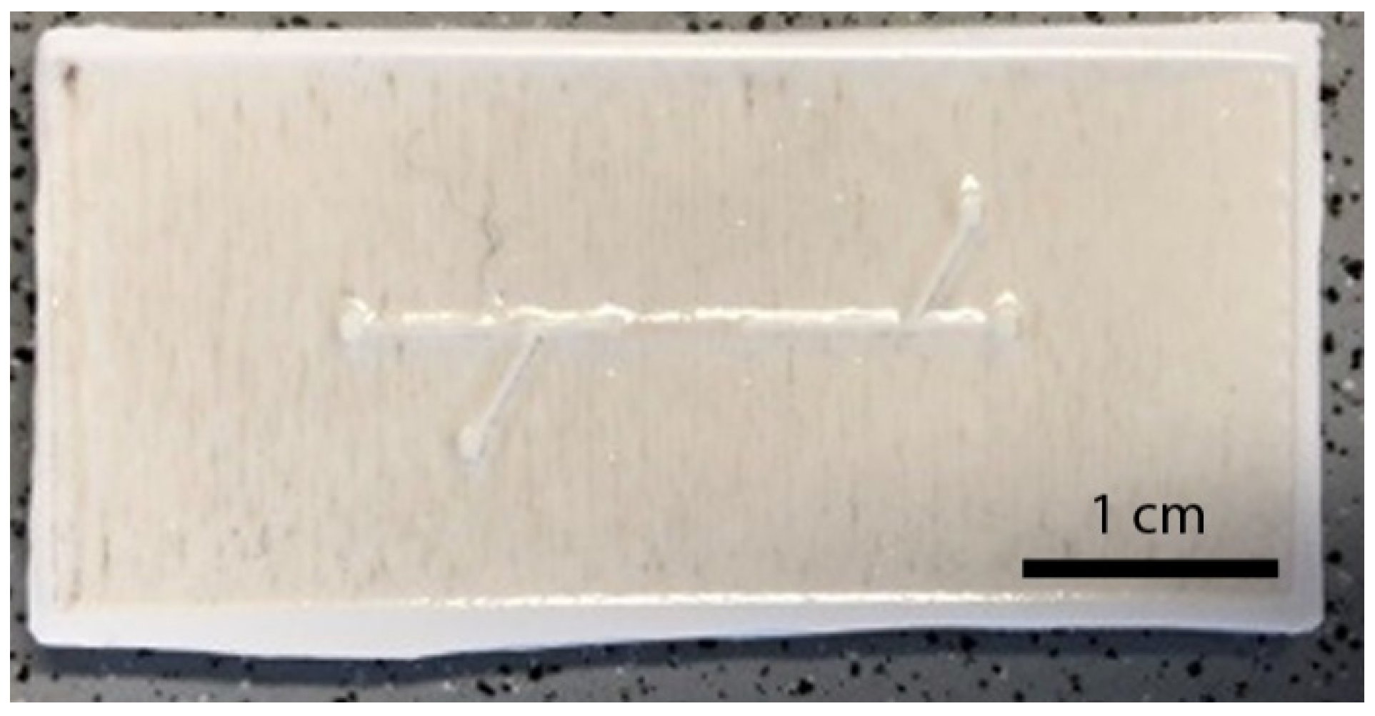
A very easy way to build casting molds for PDMS-based microfluidic systems is to simply use tape or capillaries [39,40]. To create microfluidic channels, capillaries of different sizes or tape were glued in the Petri dish (Figure 6a,b). A thin, fused silica capillary (I.D. = 100 µm, O.D. = 350 µm) was put between wider polytetrafluoroethylene fittings (I.D. = 350 µm O.D. = 1.25 mm) to obtain a sieve for particle retention. This procedure has already been used in other studies and is based on pushing capillaries into each other, whereby the inner diameter of the outer capillary must correspond exactly to the outer diameter of the inner capillary [8,17]. To create a mold with adhesive tape (polyvinyl chloride), four layers with a total thickness of 260 µm were aligned on top of each other, thereby forming the channel. Between two channels, a layer of adhesive tape with a thickness of 65 µm was used to form the sieve structure. The adhesive tape stayed adhered to the petri dish after removing the PDMS. The capillaries were pulled out of the PDMS.
Subsequently the PDMS was cut and adhered to the cover slide via plasma bonding (Figure 6c). The bonding was strong enough that separation of glass and PDMS was impossible without breaking the glass or rupturing the PDMS. The microfluidic device was connected to the tubing and fluid flow without leakage was achieved. However, the microfluidic device fabrication without mold was not continued for multiple reasons. On the one hand, spontaneous bubble formation occurred during PDMS curing, which originated from air under the tape and in the capillaries. On the other hand, it was impossible to create straight channels or to replicate chips with identical dimensions. The transitions between tapes and also between the capillaries were unstructured and not well defined (Figure 7a,b). The reproducibility of the microfluidic devices was therefore not guaranteed. Thus, other mold fabrication methods to replicate microfluidic devices with a defined design were evaluated.
3.2. Fabrication of PDMS Chips with 3D-Printed, Laser-Engraved, and Milled Casting Molds
To create casting molds with 3D printing, laser cutting, or milling, different types of sieves were designed. A microreactor casting mold with a narrow sieve with the same height as the channel and 60 µm in width and another mold with a 60 µm flat sieve with the same width as the channel was designed. Since it was initially unclear which of the designs would lead to a good result without collapsing the channel structure, both were used to start with and were validated during manufacturing.
3.2.1. 3D Printing with a Fused Deposition Modeling Printer
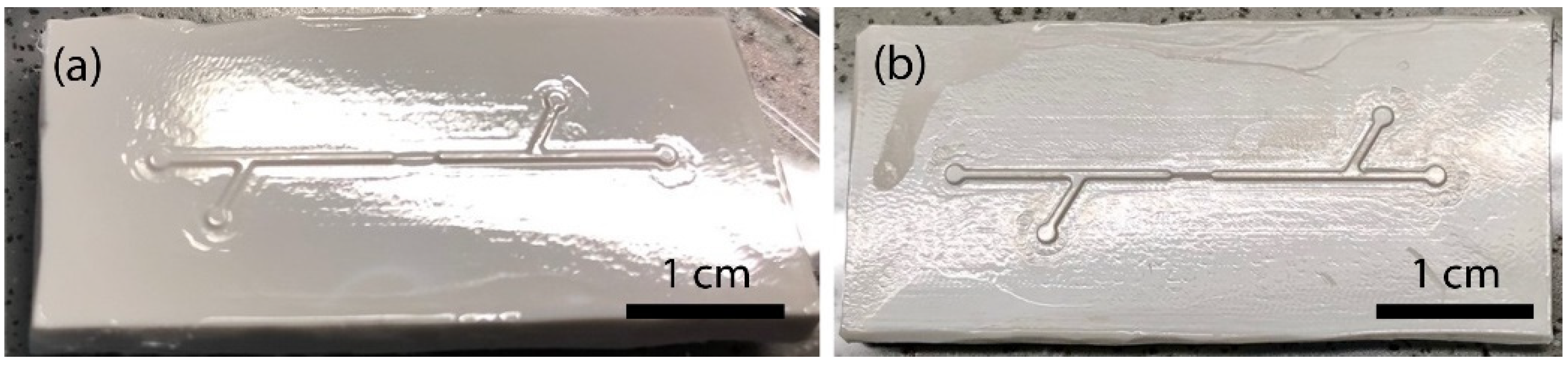
The fused deposition modeling printer, Ultimaker S5, was used to create a casting mold out of ABS. The sieve was designed to be 60 µm flat and 500 µm wide. A narrow sieve could not be created due to the printer’s limitations of a minimum of 250 µm in diameter. The printer left streaks of polymer at the ports of the casting mold, which had to be cut and filed off the casting mold (Figure 8a). The print was visualized as a microscopic 3D image showing surface roughness and a well-defined channel structure (Figure 8b).
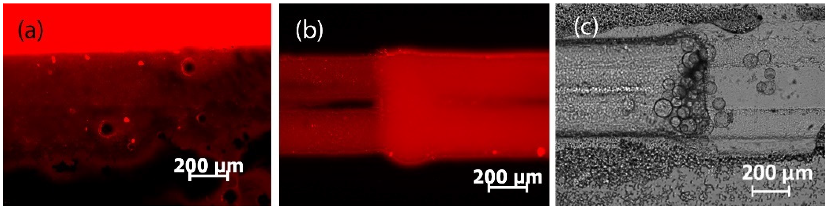
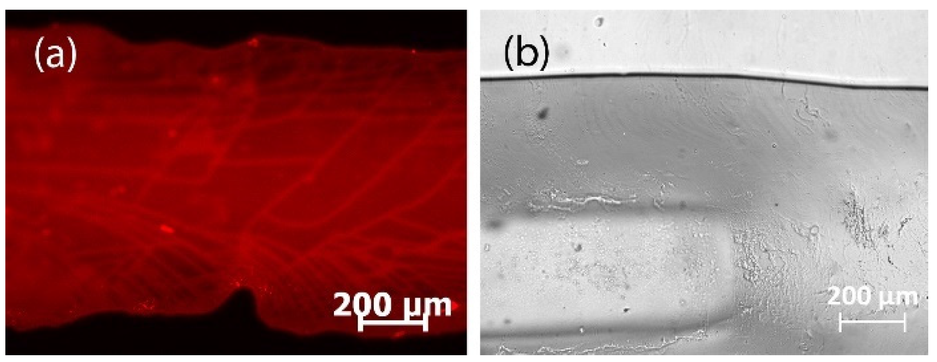
The print as well as its replica had visible grooves on the surface, which impaired the binding of the PDMS replica to the cover slide and resulted in leaks (Figure 9a). The leakage was visualized with fluorescent rhodamine B solution (Figure 9b).
The reaction chamber of the microfluidic chip was filled with spherical particles to test the retention of spherical particles. Although the chip was leaking, spherical particles were successfully retained (Figure 10a,b).
To smoothen the grooves and thereby tackle leakage, the casting mold was exposed to acetone vapor for 20 min. This resulted in a leak-tight microfluidic chip but altered the design with convexities in place of former grooves, thereby enlarging the channel width up to 1000 µm. Spherical particles were still retained (Figure 11a–c).
3.2.2. 3D Printing with a Stereolithographic Printer
The stereolithographic printer Form 2 was used to create a casting mold out of black resin. The sieve was designed to be 60 µm flat and 500 µm wide. The narrow sieve could not be created due to the printer’s limitations of a minimum of 140 µm in diameter. The casting mold and a 3D picture of the sieve are depicted in Figure 12a,b.
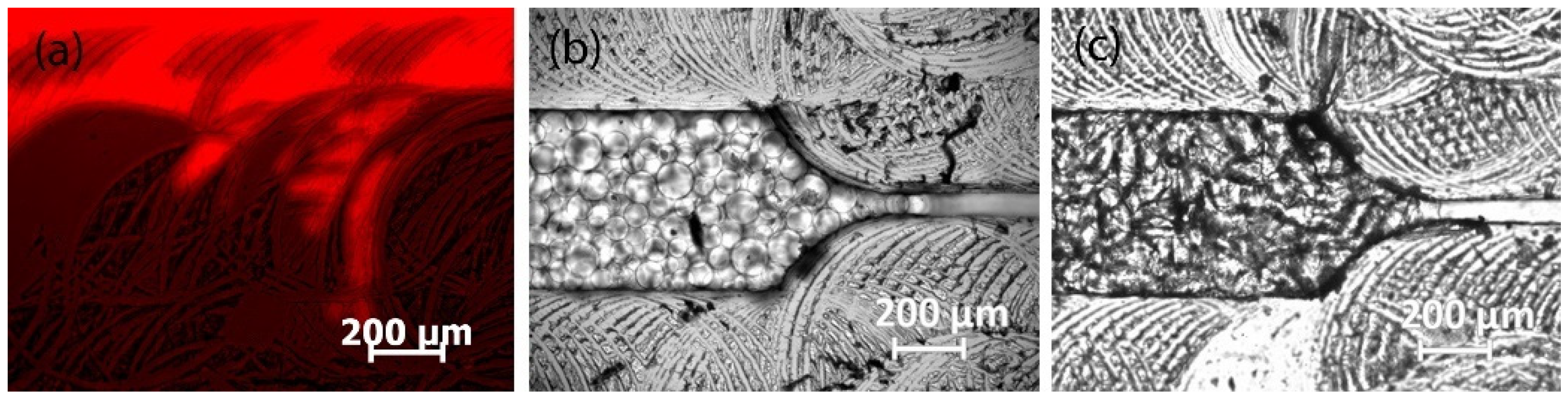
The resulting casting mold was porous. Interestingly, the subsequent curing of PDMS proceeded well, although it is known that cure inhibition is a problem with some stereolithographic resins [41,42]. The good result could be due to the long UV irradiation of 24 h, which may have reduced the leaching of monomers during PDMS curing. However, when rhodamine B solution was pumped through the microfluidic chip, leakage around the channels was observed (Figure 13a). The design of the sieve was altered by the Form 2 fabrication, thereby resulting in the printing of two separate sieves—instead of one flat and wide sieve (Figure 13b). Nevertheless, particles could be retained as shown in Figure 13c.
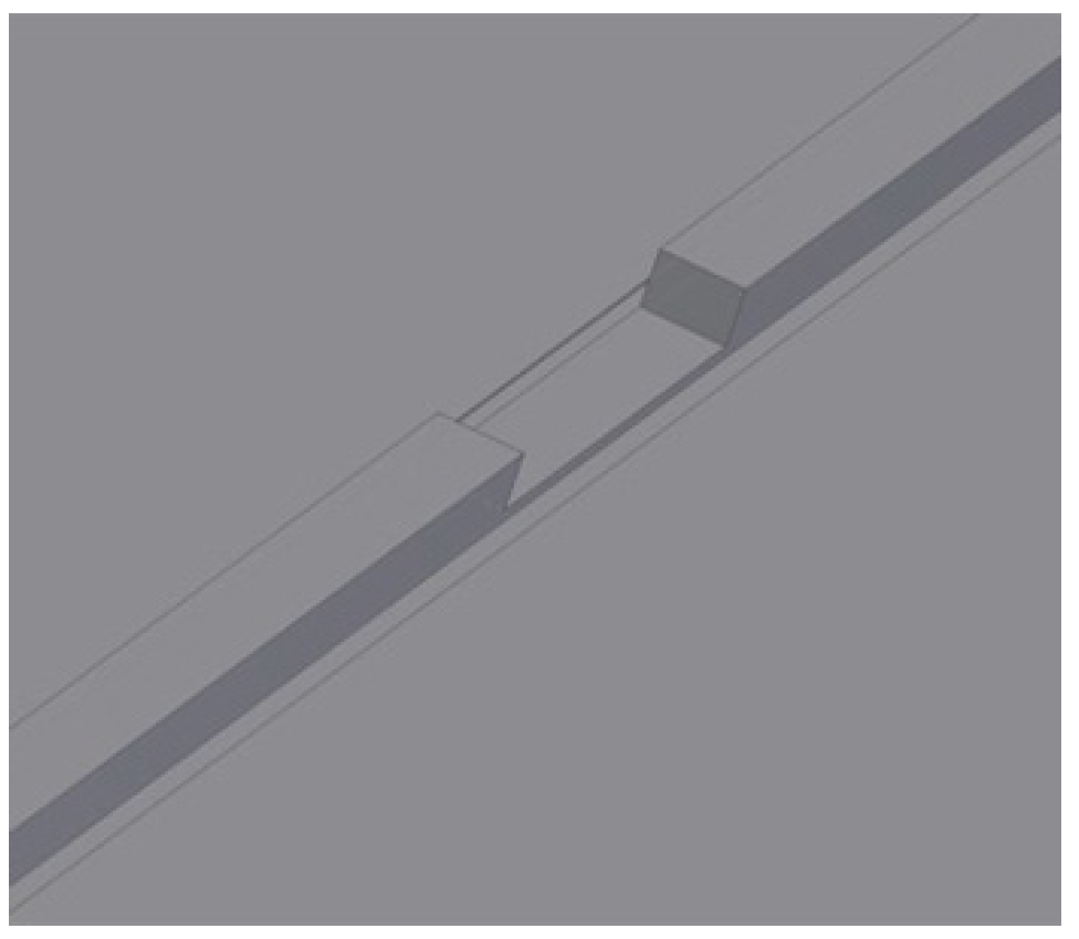
The black resin could not be polished with acetone. In order to increase the tightness, a gasket was implemented in the print design. The gasket was aligned around the channels. It was designed to be 140 µm wide and 25 µm deep in the casting mold. This created an equal 25 µm elevation around the channels in the PDMS replica (Figure 14), which was pressed onto the cover slide, thereby facilitating the binding between the glass and the PDMS.
Particle retention was still feasible, but the gasket failed at some points and leakage was observed (Figure 15a–c).
3.2.3. Laser Engraving
Laser engraving into ABS was done with the Rayjet laser engraver. The surface of the ABS was exposed to the laser omitting the desired channel structure (Figure 16). The desired design was therefore untouched by the laser. The laser was set to a power of 15 W and a speed of 30 inch per second using the software Rayjet Jobcommand.
A PDMS replica was manufactured and rhodamine B solution was subsequently perfused through the microfluidic chip (Figure 17a). Leakage was not observed, indicating good binding between the PDMS replica and the cover slide. However, the channel walls were uneven, which could cause particle clogging in channel locations where it is not desirable. The channel wall could be polished acetone vapor for 5 min, which increased the channel width to 860–925 µm (Figure 17b). Particles could not be retained after the polishing step.
3.2.4. Milling
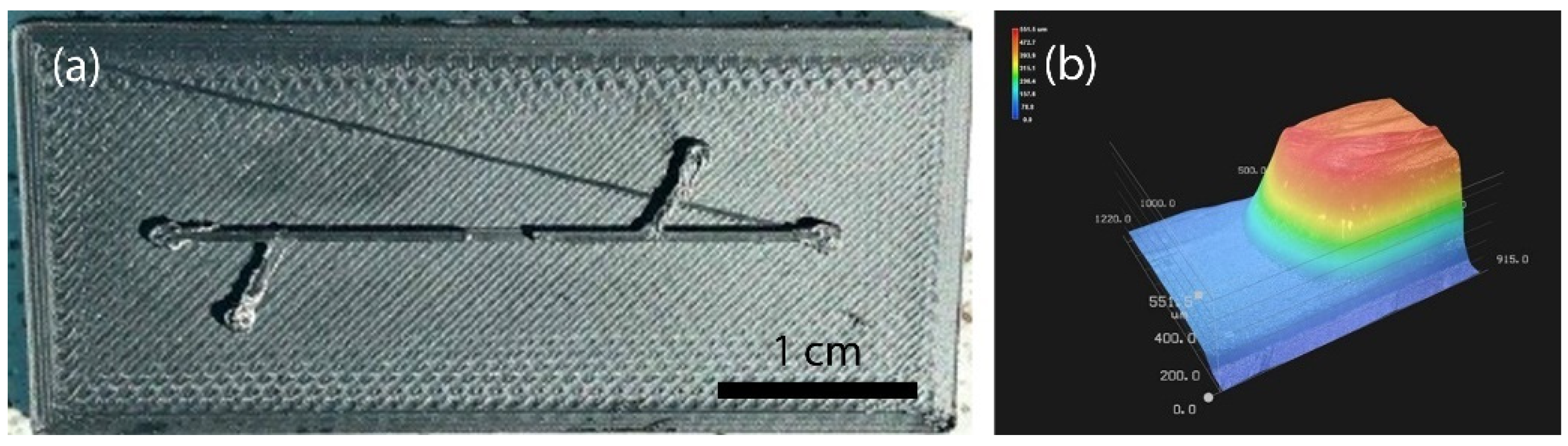
Casting molds with 60 µm flat and 500 µm wide, as well as 60 µm wide and 400 µm high sieves were fabricated with the CNC-ICP 4030 milling machine. The molds were successfully milled out of 3 mm thick, white ABS. The results and 3D microscopic pictures are shown in Figure 18a–c.
Different offsets of the milling head (0.7 mm, 0.4 mm, 0.1 mm) were used for fabrication. Even though the process time was extended by a smaller offset, the grooves were visibly reduced. Milling was carried out with an offset of 0.1 mm hereafter to obtain a smooth surface and to facilitate acetone vapor polishing. The resulting microfluidic chips were capable of spherical and non-spherical particle retention (Figure 19b,c), but some leakage around the channel was observed (Figure 19a). This leakage spread out following the geometries of the milling head.
The ABS casting molds were exposed to acetone vapor to smoothen the surface, and hence to minimize leakage of the final microfluidic chip. At first, a narrow sieve casting mold was polished for 20 min in a 70 °C heated vapor bath. Afterwards, the microfluidic chip could still be filled with particles and no leakage around the channel was observed (Figure 20a–c). However, polishing altered the structure of the channel and resulted in channels with a maximum width of 680 µm with sloping sidewalls that prevented the particles from filling the entire reaction chamber (Figure 20a). This led to a fluid flow along the sides of the channel, circumventing a flow through the particle bed. Furthermore, particles could slip through the sieve, which had a width of up to 140 µm after polishing, until they clogged or a bigger particle got stuck (Figure 20b,c).
Another design, with a 60 µm flat and 500 µm wide sieve, was chosen, so that even after acetone polishing, particles were not able to slip through the sieve, since polishing did not raise, but flatten and enlarge the structures. At first, it was tested whether the design enabled proper particle retention. Both particle types were retained by the flat sieve (Figure 21a,b). Subsequently, the casting molds were polished with acetone vapor. The time of exposure was reduced to 30 s, offering a better compromise between maximal smoothness of the surface and minimal deformation of the channels (Figure 21c).
3.2.5. Acetone Polishing
For the developed fabrication method, it is necessary to smooth the surface of the casting pattern, therefore polishing with acetone was established and optimized. Different ways of ABS polishing were tested for the casting mold fabricated by milling. Acetone polishing was done by dipping the ABS casting mold in liquid acetone as well as by exposing the mold to acetone vapor. Liquid dipping is more convenient, since acetone vapor is highly flammable. The ABS mold was dipped into the liquid acetone for 1 s. The mold was left for drying, but the acetone, which penetrated the ABS, continued to solve the ABS, thereby destroying the channels and sieve (Figure 22a). For this reason, the molds were dried with compressed gas immediately after immersion. However, this resulted in acetone droplets rolling over the ABS surface and leaving grooves (Figure 22b).
The grooves hampered binding or even altered the design, and it was not possible to create a reproducible replica. Subsequently, acetone vapor polishing was tested. The setup and a resulting polished casting mold are shown in Figure 23a,b. An amount of 30 mL of acetone was heated at 70 °C, filling the glass jar with acetone vapor. Paper towels were aligned to the sides to enable the acetone to raise up the towels and thereby facilitate an even vapor distribution throughout the jar. The jar was closed off with a glass cover. The molds were exposed to acetone vapor for 30 s, 1 min, 2 min, 5 min, and 20 min. An exposure of 30 s was sufficient to facilitate proper binding without leakage between PDMS replicas and the glass cover slides.
We also measured the changes in the channel height, which was normalized to the target depth, and the arithmetic average roughness Ra (Table 1). The longer the casting mold was exposed to acetone vapor, the more the height of the channels deviated from the target height. The original channel height of the milled structure without polishing did not deviate from the target height. The roughness of 2.2 ± 0.7 µm of the original part was reduced to 0.3 ± 0.1 µm by 30 s acetone vapor treatment. Further acetone polishing resulted in roughness values too low for quantification.
4. Discussion
Many different methods were developed to fabricate microfluidic chips in the past [43]. One of the most common techniques is based on photolithography for structures with a diameter of 30 nm–100 mm. Nano-imprint lithography can even reach diameters of 5 nm [44]. However, these methods have sophisticated requirements, such as photomask fabrication and projecting systems [45]. Since, in this study, the main task of the microfluidic chip was to retain particles larger than 60 µm in diameter, such precise methods were not needed and therefore simpler and cheaper methods were investigated. The creation of casting templates by capillary and tape was quickly discarded, as it was too inaccurate and not reproducible. Although it has been shown that capillaries and tape can be used to create molds for PDMS chips [39,40], our experiments were not successful. Nevertheless, for two-dimensional structures, this method seems to be useful [46]. The methods used for a more defined fabrication of a casting mold rated from laser cutting, stereolithographic 3D printing, fused deposition modelling 3D printing, and CNC milling. Each method was applied for casting mold fabrication and the obtained PDMS chip was assessed in terms of particle retention capability, leak tightness, and structural accuracy (Table 2).
Laser cutting proved to be the most unreliable method. In the literature, this process has been successfully used to produce interlayers for lamination with cut-outs for channel geometry [38]. Additionally, laser cutting can provide a method for precise and rapid prototyping, such as the fabrication of reusable PDMS molds by laser ablation [47,48]. However, it was not possible to perform the laser cutting in 3D with ABS as substrate as it was intended in our study. This made it impossible to obtain replicable casting molds with a defined flatter sieve than the surrounding channels. The laser did not create even channel walls, which inhibited the production of small sieves. Thus, particle retention failed. Nevertheless, the surface area exposed to the laser was still smooth enough to enable leak tight bonding between the PDMS replica and a glass cover slide. This method might be useful for other microfluidic structures with different requirements. In the literature, some laser-ablated methods were reported, which were used to directly engrave polymers, such as PMMA or PDMS [49]. These methods are especially rapid, easy, and cost-effective for microstructure mold fabrication [50,51].
Microfluidic chips fabricated by fused deposition modeling and stereolithographic 3D printing enabled particle retention in front of a flat sieve. Narrow screens could not be produced because the minimum diameter of the applied polymer/hardened resin exceeded the required 60 µm. On the screen itself, the structure deviated from the design because the polymer or resin could only be applied or cured as round structures. The grooves on the mold surface of fused deposition modeling (FDM)-printed molds made bonding difficult and changed the structure of the channels after acetone polishing. The grooves were not printed with the stereolithographic 3D printer, but the surface was too rough to form a good bonding and could not be polished with acetone. Resins other than the black resin could provide better results and eventually led to dense microfluidic devices. In general, 3D printed molds for PDMS chip fabrication have steadily gained attention in recent years [42,52,53]. We are therefore convinced that this method can be further optimized to produce applicable PDMS molds.
CNC milling produced the most accurate molds with the greatest variety of designs, as both flat sieves and narrow sieves could be milled. Microfluidic devices obtained from the fabrication method retained particles, but the bonding was loose, and leakage occurred over time. Bonding was enhanced and leakage was eliminated with a smoothened acetone polished casting mold, although the structure was altered minimally. Acetone polishing was done for 30 s, 1 min, 2 min, and 5 min. The best results were obtained after 30 s of polishing and, hence, less time may still be sufficient to eliminate leakage while keeping the original design. Polishing with acetone vapor can also be done at lower temperatures, but this increases the time frame for achieving the same results [54].
5. Conclusions
In this study, mold fabrication and subsequent PDMS replication were established for the fabrication of microfluidic chips. The machines used were all easier to handle and cheaper than microfluidic device fabrication through photolithography, which is the prevalent method in mold fabrication [45]. Especially, CNC milling provided the most reliable outcome, however future development of 3D printing may result in a competitively reliable casting mold fabrication. These findings can now be used for fast and easy prototyping of PDMS replicas for microfluidic device development. If reusability of the device is a major concern, one should switch to other materials, e.g., glass or ceramic, because gas-permeable PDMS is degraded by fouling over time [55], and multiple tube attachments and detachments increase the likelihood that the microfluidic PDMS device could rupture.
Author Contributions
Conceptualization, K.R.; methodology, K.R.; software, J.V.; validation, K.R.; formal analysis, J.V.; investigation, J.V.; data curation, J.V.; writing—original draft preparation, J.V. and K.R.; writing—review and editing, K.R.; visualization, J.V. and K.R.; supervision, K.R.; project administration, K.R.; funding acquisition, K.R. All authors have read and agreed to the published version of the manuscript.
Funding
This research was supported by the Max-Buchner Forschungsstiftung.
Institutional Review Board Statement
Not applicable.
Informed Consent Statement
Not applicable.
Data Availability Statement
Data are contained within the article.
Acknowledgments
We gratefully thank the team of the Makerspace, especially Marvin Hesse, of the TU Dortmund University for their support for the fabrication of casting molds. We also thank Christoph Brandenbusch for his support in the use of the Keyence microscope. We thank Frank Katzenberg for provision of equipment for plasma bonding. EnginZyme AB (Sweden) is gratefully acknowledged for the generous gift of EziGTM enzyme carriers.
Conflicts of Interest
The authors declare no conflict of interest.
References
- Schmid, A.; Hollmann, F.; Park, J.B.; Bühler, B. The use of enzymes in the chemical industry in Europe. Curr. Opin. Biotechnol. 2002, 13, 359–366. [Google Scholar] [CrossRef]
- Rosenthal, K.; Lütz, S. Recent developments and challenges of biocatalytic processes in the pharmaceutical industry. Curr. Opin. Green Sustain. Chem. 2018, 11, 58–64. [Google Scholar] [CrossRef]
- Chapman, J.; Ismail, A.E.; Dinu, C.Z. Industrial applications of enzymes: Recent advances, techniques, and outlooks. Catalysts 2018, 8, 238. [Google Scholar] [CrossRef]
- Truppo, M.D. Biocatalysis in the Pharmaceutical Industry: The Need for Speed. ACS Med. Chem. Lett. 2017, 8, 476–480. [Google Scholar] [CrossRef] [PubMed]
- Urban, P.L.; Goodall, D.M.; Bruce, N.C. Enzymatic microreactors in chemical analysis and kinetic studies. Biotechnol. Adv. 2006, 24, 42–57. [Google Scholar] [CrossRef] [PubMed]
- Manz, A.; Verpoorte, E.; Raymond, D.E.; Effenhauser, C.S.; Burggraf, N.; Widmer, H.M. µ-TAS: Miniaturized total chemical analysis systems. In Micro Total Analysis Systems; Van den Berg, A., Bergveld, P., Eds.; Springer Dordrecht: Basel, Switzerland, 1990; pp. 5–6. [Google Scholar]
- Gupta, S.; Ramesh, K.; Ahmed, S.; Kakkar, V. Lab-on-chip technology: A review on design trends and future scope in biomedical applications. Int. J. Bio-Sci. Bio-Technol. 2016, 8, 311–322. [Google Scholar] [CrossRef]
- Fritzsch, F.S.O.; Rosenthal, K.; Kampert, A.; Howitz, S.; Dusny, C.; Blank, L.M.; Schmid, A. Picoliter nDEP traps enable time-resolved contactless single bacterial cell analysis in controlled microenvironments. Lab Chip 2013, 13, 397–408. [Google Scholar] [CrossRef] [PubMed]
- Meller, K.; Szumski, M.; Buszewski, B. Microfluidic reactors with immobilized enzymes—Characterization, dividing, perspectives. Sens. Actuators B Chem. 2017, 244, 84–106. [Google Scholar] [CrossRef]
- Zhu, Y.; Chen, Q.; Shao, L.; Jia, Y.; Zhang, X. Microfluidic immobilized enzyme reactors for continuous biocatalysis. React. Chem. Eng. 2020, 5, 9–32. [Google Scholar] [CrossRef]
- Fritzsch, F.S.O.; Dusny, C.; Frick, O.; Schmid, A. Single-cell analysis in biotechnology, systems biology, and biocatalysis. Annu. Rev. Chem. Biomol. Eng. 2012, 3, 129–155. [Google Scholar] [CrossRef]
- Deng, Y.; Guo, Y.; Xu, B. Recent development of microfluidic technology for cell trapping in single cell analysis: A review. Processes 2020, 8, 1253. [Google Scholar] [CrossRef]
- Johann, R.M. Cell trapping in microfluidic chips. Anal. Bioanal. Chem. 2006, 385, 408–412. [Google Scholar] [CrossRef]
- Gale, B.K.; Jafek, A.R.; Lambert, C.J.; Goenner, B.L.; Moghimifam, H.; Nze, U.C.; Kamarapu, S.K. A review of current methods in microfluidic device fabrication and future commercialization prospects. Inventions 2018, 3, 60. [Google Scholar] [CrossRef]
- Ren, K.; Zhou, J.; Wu, H. Materials for microfluidic chip fabrication. Acc. Chem. Res. 2013, 46, 2396–2406. [Google Scholar] [CrossRef]
- Fernandes, A.C.; Gernaey, K.V.; Krühne, U. Connecting worlds—A view on microfluidics for a wider application. Biotechnol. Adv. 2018, 36, 1341–1366. [Google Scholar] [CrossRef] [PubMed]
- Rosenthal, K.; Falke, F.; Frick, O.; Dusny, C.; Schmid, A. An inert continuous microreactor for the isolation and analysis of a single microbial cell. Micromachines 2015, 6, 1836–1855. [Google Scholar] [CrossRef]
- Waldbaur, A.; Rapp, H.; Länge, K.; Rapp, B.E. Let there be chip—Towards rapid prototyping of microfluidic devices: One-step manufacturing processes. Anal. Methods 2011, 3, 2681–2716. [Google Scholar] [CrossRef]
- Joseph Fortenbaugh, R.; Lear, B.J. On-demand curing of polydimethylsiloxane (PDMS) using the photothermal effect of gold nanoparticles. Nanoscale 2017, 9, 8555–8559. [Google Scholar] [CrossRef] [PubMed]
- Johnston, I.D.; McCluskey, D.K.; Tan, C.K.L.; Tracey, M.C. Mechanical characterization of bulk Sylgard 184 for microfluidics and microengineering. J. Micromech. Microeng. 2014, 24, 035017. [Google Scholar] [CrossRef]
- Lee, J.N.; Park, C.; Whitesides, G.M. Solvent Compatibility of Poly(dimethylsiloxane)-Based Microfluidic Devices. Anal. Chem. 2003, 75, 6544–6554. [Google Scholar] [CrossRef] [PubMed]
- Lu, B.; Zheng, S.; Quach, B.Q.; Tai, Y.C. A study of the autofluorescence of parylene materials for μtAS applications. Lab Chip 2010, 10, 1826–1834. [Google Scholar] [CrossRef] [PubMed]
- Islam, M.M.; Loewen, A.; Allen, P.B. Simple, low-cost fabrication of acrylic based droplet microfluidics and its use to generate DNA-coated particles. Sci. Rep. 2018, 8, 8763. [Google Scholar] [CrossRef] [PubMed]
- Parthiban, P.; Vijayan, S.; Doyle, P.S.; Hashimoto, M. Evaluation of 3D-printed molds for fabrication of non-planar microchannels. Biomicrofluidics 2021, 15, 024111. [Google Scholar] [CrossRef] [PubMed]
- Mehta, V.; Rath, S.N. 3D printed microfluidic devices: A review focused on four fundamental manufacturing approaches and implications on the field of healthcare. Bio-Des. Manuf. 2021, 4, 311–343. [Google Scholar] [CrossRef]
- Felton, H.; Hughes, R.; Diaz-Gaxiola, A. Negligible-cost microfluidic device fabrication using 3D-printed interconnecting channel scaffolds. PLoS ONE 2021, 16, e0245206. [Google Scholar] [CrossRef]
- Bonyár, A.; Sántha, H.; Varga, M.; Ring, B.; Vitéz, A.; Harsányi, G. Characterization of rapid PDMS casting technique utilizing molding forms fabricated by 3D rapid prototyping technology (RPT). Int. J. Mater. Form. 2014, 7, 189–196. [Google Scholar] [CrossRef]
- Bazaz, S.R.; Kashaninejad, N.; Azadi, S.; Patel, K.; Asadnia, M.; Jin, D.; Warkiani, M.E. Rapid Softlithography Using 3D-Printed Molds. Adv. Mater. Technol. 2019, 4, 1900425. [Google Scholar] [CrossRef]
- Saadat, M.; Taylor, M.; Hughes, A.; Hajiyavand, A.M. Rapid prototyping method for 3D PDMS microfluidic devices using a red femtosecond laser. Adv. Mech. Eng. 2020, 12, 1–12. [Google Scholar] [CrossRef]
- Li, H.; Fan, Y.; Foulds, I.G. Rapid and low-cost fabrication of polystyrene-based molds for PDMS microfluidic devices using a CO2 laser. Adv. Mater. Res. 2012, 403–408, 4344–4348. [Google Scholar] [CrossRef]
- Qin, S.; Ou, G.; Wang, B.; Li, Z.; Hu, R.; Li, Y.; Yang, Y. Photolithography-free fabrication of photoresist-mold for rapid prototyping of microfluidic PDMS devices. Chin. Chem. Lett. 2022, 33, 987–989. [Google Scholar] [CrossRef]
- Srinivasan, A.; Bach, H.; Sherman, D.H.; Dordick, J.S. Bacterial P450-catalyzed polyketide hydroxylation on a microfluidic platform. Biotechnol. Bioeng. 2004, 88, 528–535. [Google Scholar] [CrossRef] [PubMed]
- Hakala, T.A.; Bialas, F.; Toprakcioglu, Z.; Bräuer, B.; Baumann, K.N.; Levin, A.; Bernardes, G.J.L.; Becker, C.F.W.; Knowles, T.P.J. Continuous Flow Reactors from Microfluidic Compartmentalization of Enzymes within Inorganic Microparticles. ACS Appl. Mater. Interfaces 2020, 12, 32951–32960. [Google Scholar] [CrossRef] [PubMed]
- Brás, E.J.S.; Domingues, C.; Chu, V.; Fernandes, P.; Conde, J.P. Microfluidic bioreactors for enzymatic synthesis in packed-bed reactors—Multi-step reactions and upscaling. J. Biotechnol. 2020, 323, 24–32. [Google Scholar] [CrossRef]
- Lalehpour, A.; Barari, A. Post processing for Fused Deposition Modeling Parts with Acetone Vapour Bath. IFAC-PapersOnLine 2016, 49, 42–48. [Google Scholar] [CrossRef]
- Katzenberg, F. Plasma-bonding of poly(dimethylsiloxane) to glass. e-Polymers 2005, 5. [Google Scholar] [CrossRef]
- Satyanarayana, S.; Karnik, R.N.; Majumdar, A. Stamp-and-stick room-temperature bonding technique for microdevices. J. Microelectromech. Syst. 2005, 14, 392–399. [Google Scholar] [CrossRef]
- Walsh, D.I.; Kong, D.S.; Murthy, S.K.; Carr, P.A. Enabling Microfluidics: From Clean Rooms to Makerspaces. Trends Biotechnol. 2017, 35, 383–392. [Google Scholar] [CrossRef]
- Burgoyne, F. Rapid Prototyping of Branched Microfluidics in PDMS Using Capillaries. Available online: https://blogs.rsc.org/chipsandtips/2010/05/03/rapid-prototyping-of-branched-microfluidics-in-pdms-using-capillaries/?doing_wp_cron=1544012376.7141489982604980468750 (accessed on 30 November 2021).
- Burgoyne, F. A Method for Rapid Fabrication of Microfluidic Devices. Available online: https://blogs.rsc.org/chipsandtips/2009/06/30/a-method-for-rapid-fabrication-of-microfluidic-devices/ (accessed on 30 November 2021).
- Venzac, B.; Deng, S.; Mahmoud, Z.; Lenferink, A.; Costa, A.; Bray, F.; Otto, C.; Rolando, C.; Le Gac, S. PDMS Curing Inhibition on 3D-Printed Molds: Why? Also, How to Avoid It? Anal. Chem. 2021, 93, 7180–7187. [Google Scholar] [CrossRef]
- de Almeida Monteiro Melo Ferraz, M.; Nagashima, J.B.; Venzac, B.; Le Gac, S.; Songsasen, N. 3D printed mold leachates in PDMS microfluidic devices. Sci. Rep. 2020, 10, 994. [Google Scholar] [CrossRef]
- Scott, S.M.; Ali, Z. Fabrication methods for microfluidic devices: An overview. Micromachines 2021, 12, 319. [Google Scholar] [CrossRef]
- Qian, T.; Wang, Y. Micro/nano-fabrication technologies for cell biology. Med. Biol. Eng. Comput. 2010, 48, 1023–1032. [Google Scholar] [CrossRef] [PubMed]
- Tran, K.T.M.; Nguyen, T.D. Lithography-based methods to manufacture biomaterials at small scales. J. Sci. Adv. Mater. Devices 2017, 2, 1–14. [Google Scholar] [CrossRef]
- Shrirao, A.B.; Hussain, A.; Cho, C.H.; Perez-Castillejos, R. Adhesive-tape soft lithography for patterning mammalian cells: Application to wound-healing assays. Biotechniques 2012, 52, 315–318. [Google Scholar] [CrossRef] [PubMed]
- Zhang, X.; Yao, Z.; Hou, Z.; Song, J. Processing and Profile Control of Microhole Array for PDMS Mask with Femtosecond Laser. Micromachines 2022, 13, 340. [Google Scholar] [CrossRef] [PubMed]
- Isiksacan, Z.; Guler, M.T.; Aydogdu, B.; Bilican, I.; Elbuken, C. Rapid fabrication of microfluidic PDMS devices from reusable PDMS molds using laser ablation. J. Micromech. Microeng. 2016, 26, 035008. [Google Scholar] [CrossRef]
- Lin, L.; Chung, C.K. PDMS microfabrication and design for microfluidics and sustainable energy application: Review. Micromachines 2021, 12, 1350. [Google Scholar] [CrossRef]
- Pattanayak, P.; Singh, S.K.; Gulati, M.; Vishwas, S.; Kapoor, B.; Chellappan, D.K.; Anand, K.; Gupta, G.; Jha, N.K.; Gupta, P.K.; et al. Microfluidic chips: Recent advances, critical strategies in design, applications and future perspectives. Microfluid. Nanofluid. 2021, 25, 99. [Google Scholar] [CrossRef]
- Lv, X.; Geng, Z.; Fan, Z.; Wang, S.; Su, Y.; Fang, W.; Pei, W.; Chen, H. Route to one-step microstructure mold fabrication for PDMS microfluidic chip. AIP Adv. 2018, 8, 045207. [Google Scholar] [CrossRef]
- Gyimah, N.; Scheler, O.; Rang, T.; Pardy, T. Can 3d printing bring droplet microfluidics to every lab?—A systematic review. Micromachines 2021, 12, 339. [Google Scholar] [CrossRef]
- Comina, G.; Suska, A.; Filippini, D. PDMS lab-on-a-chip fabrication using 3D printed templates. Lab Chip 2014, 14, 424–430. [Google Scholar] [CrossRef]
- Mazlan, S.N.H.; Alkahari, M.R.; Ramli, F.R.; Maidin, N.A.; Sudin, M.N.; Zolkaply, A.R. Surface finish and mechanical properties of FDM part after blow cold vapor treatment. J. Adv. Res. Fluid Mech. Therm. Sci. 2018, 48, 148–155. [Google Scholar]
- Schoenitz, M.; Grundemann, L.; Augustin, W.; Scholl, S. Fouling in microstructured devices: A review. Chem. Commun. 2015, 51, 8213–8228. [Google Scholar] [CrossRef] [PubMed]
Figure 1.
Cured polydimethylsiloxane (PDMS) with a ratio of 10:1 to its curing agent.

Figure 2.
Different microfluidic chip designs in Inventor Professional 2012. (a) Constriction in width (60 µm). (b) Constriction in height (60 µm). Magnification of (c) the constriction in width (60 µm), and (d) constriction in height (60 µm).
Figure 2.
Different microfluidic chip designs in Inventor Professional 2012. (a) Constriction in width (60 µm). (b) Constriction in height (60 µm). Magnification of (c) the constriction in width (60 µm), and (d) constriction in height (60 µm).

Figure 3.
Particles used for the chip application. (a) Non-spherical particles. (b) Spherical particles. Pictures are 40× magnified.
Figure 3.
Particles used for the chip application. (a) Non-spherical particles. (b) Spherical particles. Pictures are 40× magnified.

Figure 4.
Cases for PDMS pouring. (a) Cases with adhesive tape. (b) Polylactic acid (PLA) cases with a 90° upstand. (c) PLA cases with a 130°, 120° and 110° side wall inclination angle.
Figure 4.
Cases for PDMS pouring. (a) Cases with adhesive tape. (b) Polylactic acid (PLA) cases with a 90° upstand. (c) PLA cases with a 130°, 120° and 110° side wall inclination angle.

Figure 5.
Set-up of the microfluidic chip analysis. (a) Overall set-up of the microfluidic device including the syringe pumps as liquid reservoirs and the chip on the microscope. (b) Chip mounted on the microscope with liquid inlet and outlet.
Figure 5.
Set-up of the microfluidic chip analysis. (a) Overall set-up of the microfluidic device including the syringe pumps as liquid reservoirs and the chip on the microscope. (b) Chip mounted on the microscope with liquid inlet and outlet.

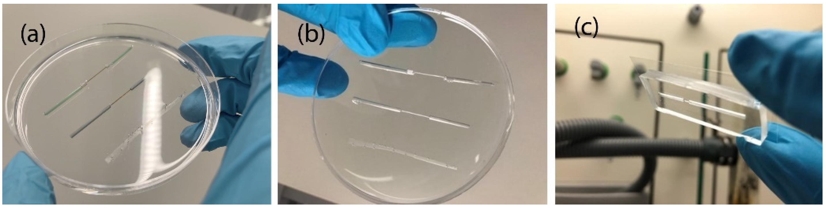
Figure 6.
PDMS fabrication methods using capillaries and tape. (a) Capillaries and adhesive tape coated with PDMS. (b) Hardened PDMS with removed capillaries and adhesive tape. (c) Structured PDMS bonded to glass.
Figure 6.
PDMS fabrication methods using capillaries and tape. (a) Capillaries and adhesive tape coated with PDMS. (b) Hardened PDMS with removed capillaries and adhesive tape. (c) Structured PDMS bonded to glass.

Figure 7.
Microfluidic chip from capillaries (a) and adhesive tape (b) at 10× magnification.

Figure 8.
Casting mold fabricated out of ABS with the Ultimaker S5. (a) Casting mold. (b) 3D picture of the sieve taken from the casting mold at the transition of the lower to the higher channel structure.
Figure 8.
Casting mold fabricated out of ABS with the Ultimaker S5. (a) Casting mold. (b) 3D picture of the sieve taken from the casting mold at the transition of the lower to the higher channel structure.

Figure 9.
Surface area, next to a channel, of a microfluidic chip replicated from a casting mold fabricated with the Ultimaker S5. (a) 10× magnified. (b) 10× magnified with fluorescence visualization of rhodamine B solution—fluid flow along the grooves leaking from the channel at the upper side of the picture.

Figure 10.
Sieve structure and particle retention with a microfluidic chip fabricated with the Ultimaker S5. (a) Sieve structure. (b) Sieve structure with retained spherical particles (Ø: 45–165 μm).
Figure 10.
Sieve structure and particle retention with a microfluidic chip fabricated with the Ultimaker S5. (a) Sieve structure. (b) Sieve structure with retained spherical particles (Ø: 45–165 μm).

Figure 11.
Sieve of a microfluidic chip replicated from a casting mold exposed to acetone vapor. (a) Sieve structure. (b) Surface next to the channel. (c) Sieve structure with retained spherical particles.
Figure 11.
Sieve of a microfluidic chip replicated from a casting mold exposed to acetone vapor. (a) Sieve structure. (b) Surface next to the channel. (c) Sieve structure with retained spherical particles.

Figure 12.
Casting mold fabricated out of black resin with the Form 2. (a) Casting mold and (b) 3D picture of the sieve taken from the casting mold at the transition of the lower to the higher channel structure.
Figure 12.
Casting mold fabricated out of black resin with the Form 2. (a) Casting mold and (b) 3D picture of the sieve taken from the casting mold at the transition of the lower to the higher channel structure.

Figure 13.
Microfluidic chip replicated from a Form 2-printed casting mold. (a) Leakage around channels visualized with fluorescent rhodamine B solution. (b) Sieve visualized with fluorescent rhodamine B solution. (c) Sieve with retained particles.
Figure 13.
Microfluidic chip replicated from a Form 2-printed casting mold. (a) Leakage around channels visualized with fluorescent rhodamine B solution. (b) Sieve visualized with fluorescent rhodamine B solution. (c) Sieve with retained particles.

Figure 14.
Inventor Professional 2012 design of a gasket (140 µm wide and 25 µm deep) aligned to the channel and sieve.
Figure 14.
Inventor Professional 2012 design of a gasket (140 µm wide and 25 µm deep) aligned to the channel and sieve.

Figure 15.
Microfluidic chip replicated from a Form 2 printed casting mold including a gasket. (a) Gasket between the channel (upper part) and leaky bond of glass and PDMS. (b) Sieve with retained particles. (c) Leakage around channels visualized with fluorescent rhodamine B solution.
Figure 15.
Microfluidic chip replicated from a Form 2 printed casting mold including a gasket. (a) Gasket between the channel (upper part) and leaky bond of glass and PDMS. (b) Sieve with retained particles. (c) Leakage around channels visualized with fluorescent rhodamine B solution.

Figure 16.
ABS casting mold fabricated with laser exposure.

Figure 17.
Microfluidic chip replicated from a laser-engraved casting mold. (a) Non-leaky channel visualized with fluorescent rhodamine B solution. (b) Enlarged channel after acetone vapor polishing.
Figure 17.
Microfluidic chip replicated from a laser-engraved casting mold. (a) Non-leaky channel visualized with fluorescent rhodamine B solution. (b) Enlarged channel after acetone vapor polishing.

Figure 18.
ABS casting molds fabricated with a milling machine. (a) Different offsets of 0.1 mm, 0.4 mm, and 0.7 mm from left to right. (b) Narrow sieve 3D picture. (c) Flat sieve 3D picture taken from the casting mold at the transition of the lower to the higher channel structure.
Figure 18.
ABS casting molds fabricated with a milling machine. (a) Different offsets of 0.1 mm, 0.4 mm, and 0.7 mm from left to right. (b) Narrow sieve 3D picture. (c) Flat sieve 3D picture taken from the casting mold at the transition of the lower to the higher channel structure.

Figure 19.
Microfluidic chip replica fabricated through milling on ABS. (a) Leakage visualized with fluorescent rhodamine B solution. (b) Narrow sieve retaining spherical particles. (c) Narrow sieve retaining non-spherical particles.
Figure 19.
Microfluidic chip replica fabricated through milling on ABS. (a) Leakage visualized with fluorescent rhodamine B solution. (b) Narrow sieve retaining spherical particles. (c) Narrow sieve retaining non-spherical particles.

Figure 20.
Microfluidic chip replica fabricated through milling on ABS and polished in acetone vapor. (a) Channel filled with non-spherical particles. (b) Narrow sieve retaining non-spherical particles. (c) Narrow sieve retaining spherical particles.
Figure 20.
Microfluidic chip replica fabricated through milling on ABS and polished in acetone vapor. (a) Channel filled with non-spherical particles. (b) Narrow sieve retaining non-spherical particles. (c) Narrow sieve retaining spherical particles.

Figure 21.
Microfluidic chip replica fabricated through milling on ABS. (a) Flat sieve retaining spherical particles. (b) Flat sieve retaining non-spherical particles. (c) Acetone polished flat sieve retaining non-spherical particles.
Figure 21.
Microfluidic chip replica fabricated through milling on ABS. (a) Flat sieve retaining spherical particles. (b) Flat sieve retaining non-spherical particles. (c) Acetone polished flat sieve retaining non-spherical particles.

Figure 22.
Acetone dipping polished casting mold fabricated through milling on ABS. (a) Mold after acetone polishing and air drying. (b) Mold after acetone polishing and pressurized gas drying.
Figure 22.
Acetone dipping polished casting mold fabricated through milling on ABS. (a) Mold after acetone polishing and air drying. (b) Mold after acetone polishing and pressurized gas drying.

Figure 23.
Acetone polishing of ABS casting molds fabricated by milling. (a) ABS casting mold exposed to acetone vapor for 30 s. (b) Setup for acetone vapor polishing.
Figure 23.
Acetone polishing of ABS casting molds fabricated by milling. (a) ABS casting mold exposed to acetone vapor for 30 s. (b) Setup for acetone vapor polishing.


Table 1.
Deviation of the channel height from target height and arithmetic average roughness Ra for different acetone vapor exposure times. n.d., not detectable.
Table 1.
Deviation of the channel height from target height and arithmetic average roughness Ra for different acetone vapor exposure times. n.d., not detectable.
| Exposure Time to Acetone Vapor | Deviation of the Channel Height | Arithmetic Average Roughness Ra |
|---|---|---|
| 0 s | 0 ± 1% | 2.2 ± 0.7 µm |
| 30 s | 3 ± 6% | 0.3 ± 0.1 µm |
| 1 min | 16 ± 9% | n.d. |
| 2 min | 11 ± 7% | n.d. |
| 5 min | 23 ± 3% | n.d. |
Table 2.
Evaluation of fabrication methods for microfluidic chip production. Laser cutting, fused deposition 3D modeling, stereolithographic 3D printing, and CNC milling are compared in regard to particle retention, leak tightness, and structural accuracy of the resulting PDMS chip. Characterized from worst (--) to best (++). (*)—after acetone polishing.
| Laser Cutting | Fused Deposition Modeling 3D Printing | Stereolithographic 3D Printing | CNC Milling | |
|---|---|---|---|---|
| Particle retention | -- | + | + | ++ |
| Leak tightness | ++ | + * | - | ++ * |
| Machine accuracy | -- | - | - | ++ |
Publisher’s Note: MDPI stays neutral with regard to jurisdictional claims in published maps and institutional affiliations. |
© 2022 by the authors. Licensee MDPI, Basel, Switzerland. This article is an open access article distributed under the terms and conditions of the Creative Commons Attribution (CC BY) license (https://creativecommons.org/licenses/by/4.0/).
Share and Cite
MDPI and ACS Style
Vogt, J.; Rosenthal, K. Validation of Easy Fabrication Methods for PDMS-Based Microfluidic (Bio)Reactors. Sci 2022, 4, 36. https://doi.org/10.3390/sci4040036
AMA Style
Vogt J, Rosenthal K. Validation of Easy Fabrication Methods for PDMS-Based Microfluidic (Bio)Reactors. Sci. 2022; 4(4):36. https://doi.org/10.3390/sci4040036
Chicago/Turabian StyleVogt, Josef, and Katrin Rosenthal. 2022. "Validation of Easy Fabrication Methods for PDMS-Based Microfluidic (Bio)Reactors" Sci 4, no. 4: 36. https://doi.org/10.3390/sci4040036