Efficient Vertical-Cavity Mid-IR Thermal Radiation to Silicon-Slab Waveguide Coupling Using a Shallow Blazed Grating †


Institute for Microelectronics and Microsensors, Johannes Kepler University Linz, 4040 Linz, Austria
*
Author to whom correspondence should be addressed.
†
Presented at the Eurosensors 2017 Conference, Paris, France, 3–6 September 2017.
Proceedings 2017, 1(4), 286; https://doi.org/10.3390/proceedings1040286
Published: 23 August 2017
(This article belongs to the Proceedings of Proceedings of Eurosensors 2017, Paris, France, 3–6 September 2017)
Abstract
:In this work we investigate the coupling of radiation originating from a vertical-cavity enhanced thermal emitter (VERTE) into an optical waveguide, which can, for instance, act as a sensing element. We present full wave modelling results demonstrating highly efficient emitter-to-waveguide diffraction coupling at multiple angles using the previously designed VERTE together with a shallow blazed grating. It is shown that the coherent and dispersive thermal emission of the VERTE concept is well suited to achieve highly efficient and integrated mode coupling in the mid IR region.
1. Introduction
On-chip optical absorption sensing poses a hard challenge to the design of all components of an optical sensor. One of the challenges is to meet required sensitivities for a specific application, as the interaction length of the light and the sensing chip is typically very small. Therefore, integrated optical sensor applications using waveguides have a high demand of achieving high intensity and narrowband guided modes in various waveguide structures in order to enhance sensitivity and specificity. We recently presented a concept and design for a vertical-cavity enhanced resonant thermal emitter (VERTE, see Figure 1a) suitable for emitting band-limited thermal radiation in the mid-infrared (mid-IR) region, which is particularly interesting for IR absorption sensing applications as it represents the so-called finger-print region where many molecules show characteristic absorption bands. Efficient coupling from the thermal emitter to a waveguide (WG) structure is a prerequisite for achieving high field intensities in the sensing regions.
The most common method for integrated waveguide coupling certainly is via a diffractive grating. Most recent investigations on grating couplers consider the coupling to/from an optical fiber mode from/into a WG mode. In our work, the coupling occurs between VERTE and WG, which leads to injection of thermal emission into a silicon slab waveguide mode. We present an analysis of an all-in-one solution demonstrating efficient coupling between the thermal emitter and a silicon slab-waveguide via a periodic diffraction grating featuring a shallow blazed profile formed at the VERTE-WG interface (Figure 2a, profile shown in the inset).
2. Simulation Configurations
2.1. 1D Frequency Domain Matrix-Transfer Method
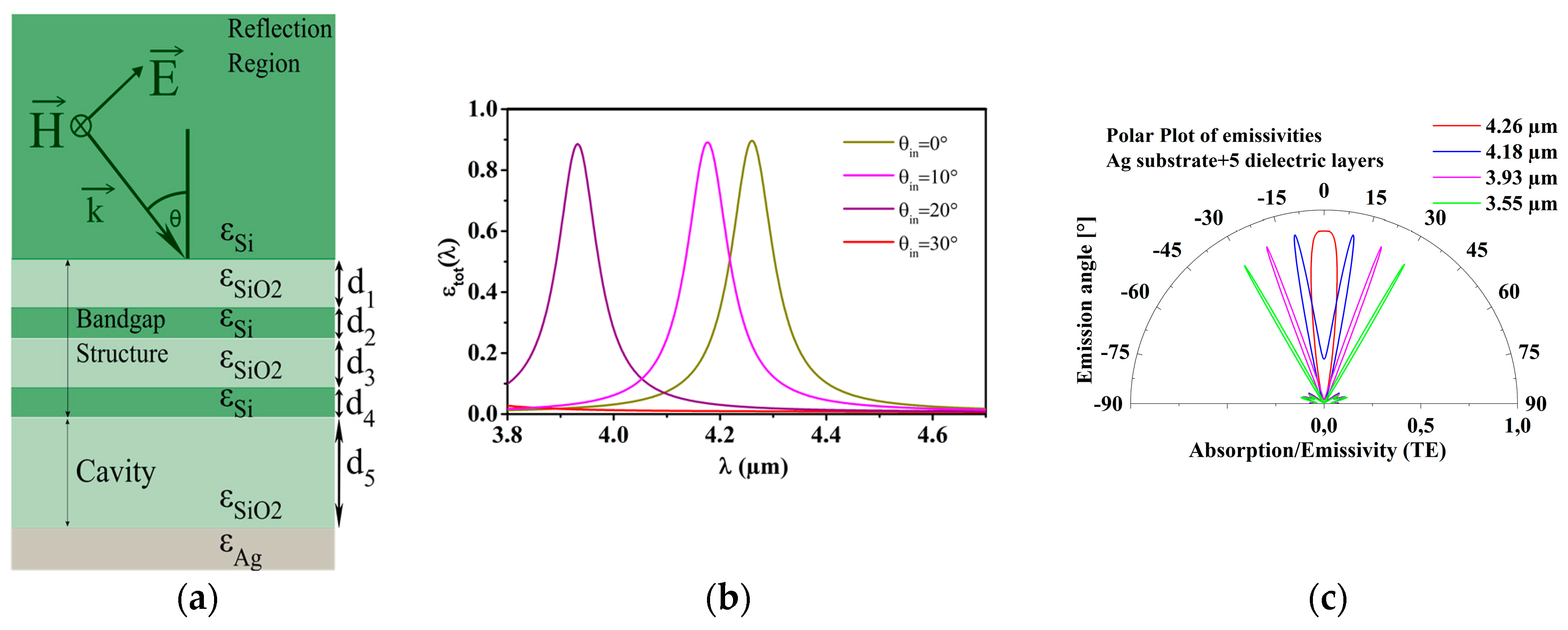
Detailed descriptions of the 1D-VERTE domains simulated by Transfer-Matrix Methods can be found elsewhere [1,2,3]. In contrast to previous works, the reflection region, i.e., the region the light is coupled into (see Figure 1a), was chosen to be silicon instead of air, which does not change the resonant (vacuum-) wavelength. Here, we focus on a five layer configuration featuring a quarter wave stack, a half-wavelength SiO2 cavity and silver as the metal layer.
2.2. 2D Frequency Domain FEM Geometry
In the 2D configuration simulated in frequency domain, the waveguide is led over the VERTE. Coupling is achieved by forming a shallow blazed grating at the waveguide-multilayer interface (Figure 2a). Field enhancement in the bottom cavity layer featured in the multilayer VERTE structure leads to a selective increase of the emissivity of the metal. As it is difficult to simulate a thermal radiation source, Kirchhoff’s law and reciprocity were utilized for the simulations. Therefore, we analyze the reciprocal situation of an incoming wave at the waveguide and calculate the absorbed energy fraction in the metal layer of the VERTE structure. Thus, a guided mode (TE) enters the slab waveguide from the input port (see Figure 2a) and the energy fractions corresponding to reflection, transmission and absorption can be written as
where R denotes the power reflected back to the input port, T is the transmission to the output port and A is the total power absorbed in the simulated domain. Assuming the absorption is negligible in Si and SiO2 (which is a good approximation in the mid IR region), the total absorption A can be written as A = AMetal + ATop with AMetal being the absorbed intensity in the silver layer and ATop being the intensity of the free space radiation absorbed by the top boundary of the simulation model. As can be seen in Figure 2a, the top boundary is the only one with absorbing properties. Perfect electric conducting boundaries at the remaining side walls ensure that there are no further absorbing losses in the simulated domain. By Kirchhoff’s law (see e.g., [3]), the fraction absorbed by the metal AMetal(θ,λ) at a specific wavelength λ and angle θ is equal to the emittance (θ,λ) of the stack configuration with respect to radiation into the WG at thermal equilibrium. Thus, in terms of reciprocity AMetal(θ,λ) = (θ,λ) corresponds to the energy fraction coupled into the waveguide from a cavity mode created by thermal radiation when it is used as an emitter.
R + T + A = 1
2.3. Coupling Efficiency
The efficiency of the coupling is now determined by two main individual features: The first one is the angular matching between the grating diffraction angle and the directional pattern of the VERTE structure (Figure 2b). As the VERTE concept can also feature very individual stack configurations with varying layer numbers and layer thicknesses, also different dispersion behavior can be achieved [3]. The dispersion behavior of the grating can be estimated from the grating Equation (4)
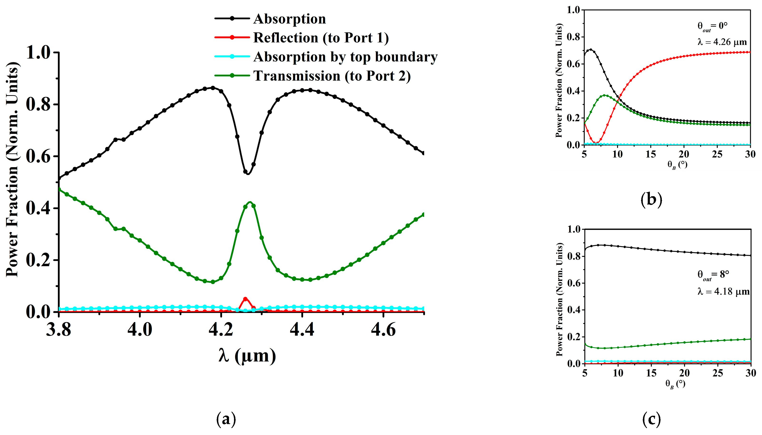
where represents the refractive indices of the waveguide and the cavity layer material, respectively. is the grating period, m the diffraction order and θin the incident angle related to the incoming WG-mode. The second factor for the coupling efficiency is the absolute intensity coupled into the desired diffraction mode order (m). In order to increase the coupling efficiency, a blazed grating profile was investigated featuring an empirically optimized blaze angle θB = 6.9°, which minimizes the back-reflection diffraction order (m) to the input port (see Figure 3a,b and Figure 4b,c). The height of the grating triangles was set to h = 100 nm and was optimized such that vertical coupling occurred at a wavelength λ = 4.26 µm ( = 1.47 µm for slab-WG height hWG = 0.66 µm). The simulated domain considered 60 periods of the grating.
3. Results and Discussion
3.1. Transfer Matrix Method 1D Simulations
The results of the 1D-simulations for the simple quarter-wave layer stack configuration without a grating on top can be seen in Figure 1b,c. It can be seen that for an emission angle θ = 10° the resonant wavelength decreases down to 4.18 µm without significant loss of emission performance ). Figure 1c shows a significant narrowing of the angular bandwidth for wavelengths corrsponding to increasing emission angles. This property suggests an increasing coupling efficiency for increasing emission angles, as a more directional emission is leads to an increased coherence length see, e.g., [1].
3.2. FEM 2D Simulations
Figure 3a,b shows the field distribution for incoming guided modes at two different wavelengths, which correspond to (a) vertical coupling (θout = 0°) and (b) small angle coupling (θout ~ 8°). It can be seen that high field intensities can be created in the cavity layer of the VERTE structure. However, the high field intensity at the output port and the green line in Figure 4a show a high transmission, thus back-coupling into the waveguide. In contrast, the 8°-coupling reaches the absorption performance suggested by the 1D simulations (, see Figure 1b,c). The cyan curve shows that the power absorbed by the top boundary ATop is very small compared to A. Thus, A is mainly determined by AMetal.
Acknowledgments
This project has been supported by the COMET K1 centre ASSIC Austrian Smart Systems Integration Research Center. The COMET—Competence Centers for Excellent Technologies-Programme is supported by BMVIT, BMWFW and the federal provinces of Carinthia and Styria.
Conflicts of Interest
The authors declare no conflict of interest. The founding sponsors had no role in the design of the study; in the collection, analyses, or interpretation of data; in the writing of the manuscript, and in the decision to publish the results.
References
- Celanovic, I.; Perreault, D.; Kassakian, J. Resonant-cavity enhanced thermal emission. Phys. Rev. B 2005, 72, 2–7. [Google Scholar] [CrossRef]
- Pühringer, G.; Jakoby, B. Modeling of a Highly Optimizable Vertical-Cavity Thermal Emitter for the Mid-Infrared. Procedia Eng. 2016, 168, 1214–1218. [Google Scholar] [CrossRef]
- Granier, C.H.; Afzal, F.O.; Min, C.; Dowling, J.P.; Veronis, G. Optimized aperiodic highly directional narrowband infrared emitters. J. Opt. Soc. Am. B 2014, 31, 1316–1321. [Google Scholar] [CrossRef]
- Covey, J.; Chen, R.T. Efficient perfectly vertical fiber-to-chip grating coupler for silicon horizontal multiple slot waveguides. Opt. Express 2013, 21, 10886–10896. [Google Scholar] [CrossRef] [PubMed]
Figure 1.
(a) 1D configuration of the 5 layer VERTE stack (without grating) (b) Corresponding emissivities at different wavelengths and (c) emission angles. Upon varying the resonant wavelength, the emissivity keeps its maximum, but its emission angle increases with narrowing angular bandwidth.
Figure 1.
(a) 1D configuration of the 5 layer VERTE stack (without grating) (b) Corresponding emissivities at different wavelengths and (c) emission angles. Upon varying the resonant wavelength, the emissivity keeps its maximum, but its emission angle increases with narrowing angular bandwidth.

Figure 2.
(a) Sketch of the simulated 2D-FEM domain (VERTE-Waveguide); (b) Angles of selected grating diffraction mode (blue) and peak emittance of the VERTE main lobe (red) versus wavelength.
Figure 2.
(a) Sketch of the simulated 2D-FEM domain (VERTE-Waveguide); (b) Angles of selected grating diffraction mode (blue) and peak emittance of the VERTE main lobe (red) versus wavelength.
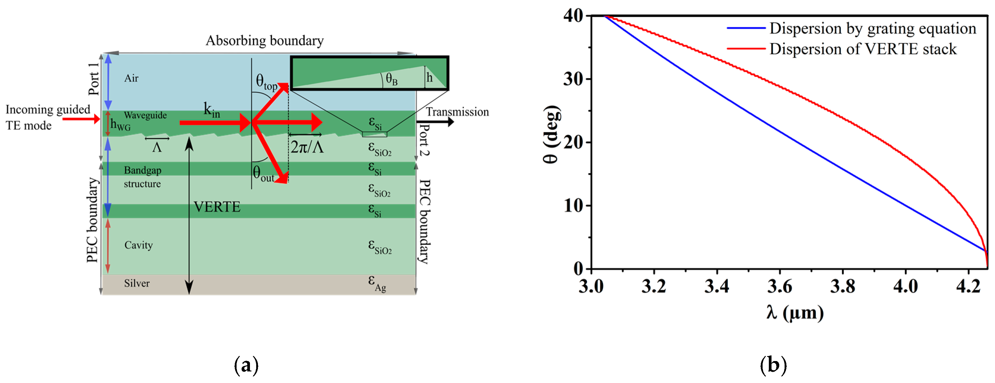
Figure 3.
Total field distribution of the E-field z-component for an incoming vacuum-wavelength of (a) 4.26 µm leading to vertical coupling and (b) 4.18 µm leading to ~8° coupling. The grating period was kept constant at 1.48 µm (60 periods were considered).
Figure 3.
Total field distribution of the E-field z-component for an incoming vacuum-wavelength of (a) 4.26 µm leading to vertical coupling and (b) 4.18 µm leading to ~8° coupling. The grating period was kept constant at 1.48 µm (60 periods were considered).
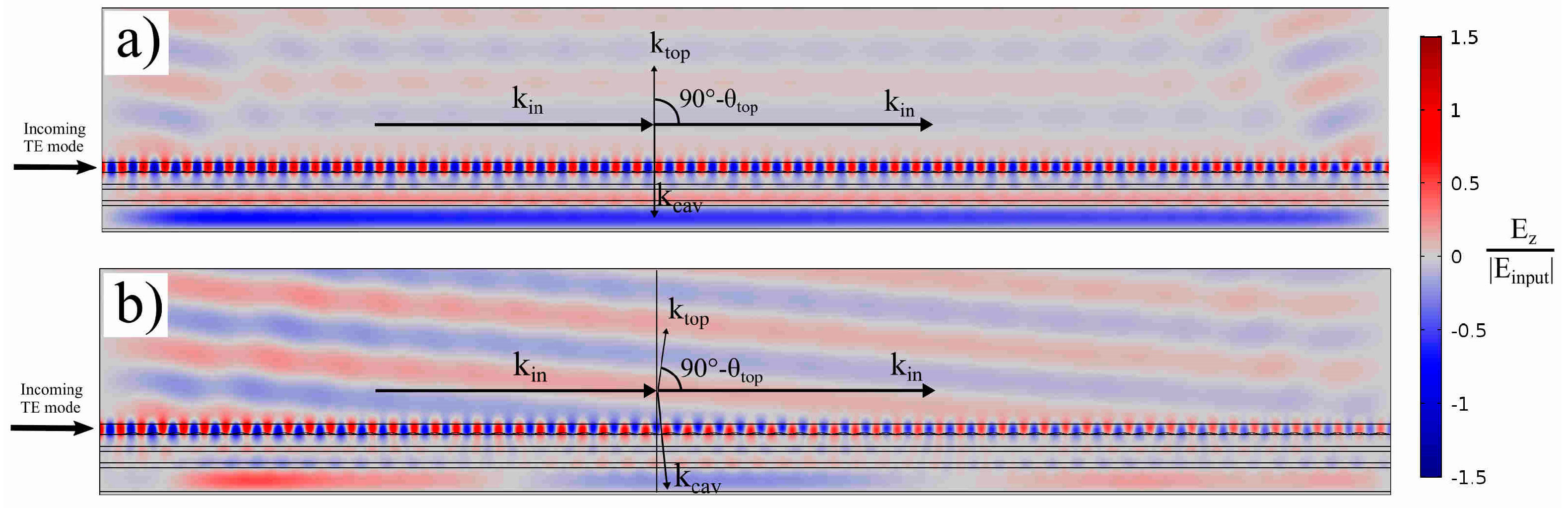
Figure 4.
(a) The black curve shows a near 90% absorption at ~4.18 µm, corresponding to a coupling angle θout ~8°. (b) and (c) show the absorption behavior at two different coupling angles (0° and 8°) for varying blaze angles θB.
Figure 4.
(a) The black curve shows a near 90% absorption at ~4.18 µm, corresponding to a coupling angle θout ~8°. (b) and (c) show the absorption behavior at two different coupling angles (0° and 8°) for varying blaze angles θB.

Publisher’s Note: MDPI stays neutral with regard to jurisdictional claims in published maps and institutional affiliations. |
© 2017 by the authors. Licensee MDPI, Basel, Switzerland. This article is an open access article distributed under the terms and conditions of the Creative Commons Attribution (CC BY) license (https://creativecommons.org/licenses/by/4.0/).
Share and Cite
MDPI and ACS Style
Pühringer, G.; Jakoby, B. Efficient Vertical-Cavity Mid-IR Thermal Radiation to Silicon-Slab Waveguide Coupling Using a Shallow Blazed Grating. Proceedings 2017, 1, 286. https://doi.org/10.3390/proceedings1040286
AMA Style
Pühringer G, Jakoby B. Efficient Vertical-Cavity Mid-IR Thermal Radiation to Silicon-Slab Waveguide Coupling Using a Shallow Blazed Grating. Proceedings. 2017; 1(4):286. https://doi.org/10.3390/proceedings1040286
Chicago/Turabian StylePühringer, Gerald, and Bernhard Jakoby. 2017. "Efficient Vertical-Cavity Mid-IR Thermal Radiation to Silicon-Slab Waveguide Coupling Using a Shallow Blazed Grating" Proceedings 1, no. 4: 286. https://doi.org/10.3390/proceedings1040286