Fabrication of ZnO Nanorods on MEMS Piezoresistive Silicon Microcantilevers for Environmental Monitoring †

 , , ,
, , , 
Abstract
:1. Introduction
2. Experimental
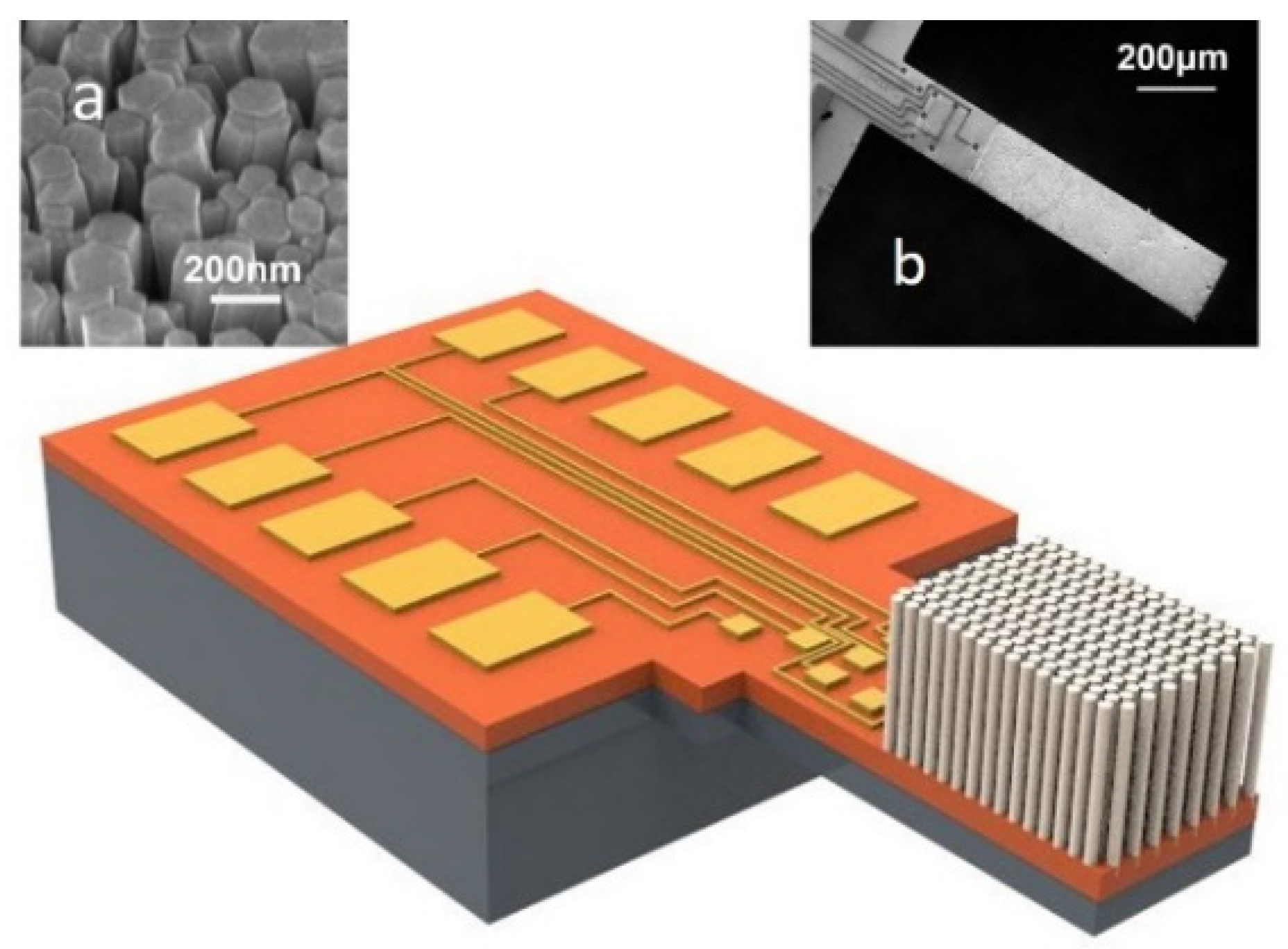
2.1. Fabrication of ZnO NRs Patterned Self-Resonant Micro-Cantilever
- (a)
- The fabrication started from a piece of sample with a dimension of 30 × 30 mm2 cut from an n-type bulk-silicon wafer (crystal orientation: <100>; resistivity: 1–10 Ω·cm; thickness: 275 ± 15 μm and diameter: 100 ± 0.13 mm). Comparing to silicon-on-insulator (SOI) wafers, the bulk silicon is preferred because of its lower price, high mechanical quality factor and larger flexibility for geometrical resonant micro-cantilever designing.
- (b)
- A 300 nm thick SiO2 layer was subsequently grown during a thermal oxidation process. The oxidation step was carried out by putting the sample into a furnace with a constant temperature of 1100 °C. This oxide layer was grown and used as a mask for subsequent n+-, p- and p+- diffusions.
- (c)
- After that, a positive photoresist (AZ 5214E, Shipley) was utilized during the photolithography step and a MJB4 mask aligner (SÜSS MicroTec AG, Garching, Germany) was used to expose the pattern area. Prior to the exposure, the photoresist spin-coating procedure was run at a speed of 5000 rpm for 35 s, to create a homogenous photoresist layer of 1.5 µm in thickness. After the exposure, the sample was then dipped and developed in AZ 726 MIF developer solution (Rohm and Haas, PA, USA) for 60 s, followed by DI water rinsing and nitrogen purging. Subsequently, the sample was dipped into buffered hydrofluoric acid solution (HF, 6–7%) for 12 min to remove the oxide layer and produce the pattern area for the phosphorus spin-on emulsion coating (3000 rpm, 30 s). Finally, the n+ diffusion was performed by putting the sample into a furnace with a temperature of 1100 °C for 30 min.
- (d)
- Afterwards, patterned areas for creating the electrical structure elements of sensor (the Wheatstone bridge, the heating resistor and sampling electrode) were fabricated by a similar procedure as described in c): thermal oxidation, spin-coating, photolithography and etching. The electrical structure element on the sample were produced by spinning-on Borofilm 100 emulsion (Emulsitone Company, NJ, USA) and the following diffusion at 1100 °C for 30 min.
- (e)
- An additional boron diffusion step was performed to reduce the contact resistance between the p-doped silicon zone and the metal (i.e., ohmic contact). The p+-diffusion was implemented exactly to the square areas where the metal contact zone will be deposited.
- (f)
- Then a polycrystalline Zn film was prepared by sputtering Zn (99.99%) using high purity Ar (99.99%) gas under 50 μA direct current (DC). The sputtered Zn film was oxidized through annealing in air at 300 °C for 60 min to obtain a crystalline ZnO seed layer. The thickness of the seed layer was controlled by adjusting the sputtering time, which is 40 min in our fabrication process, and the seed layer sputtering was only applied to the micro-cantilever area.
- (g)
- After the DC-sputtering, a bilayer of 30 nm thick chromium (Cr) and 300 nm thick gold (Au) were deposited as the metallization by electron-beam physical vapor deposition, the chromium layer serves to improve the adhesion of gold and silicon.
- (h)
- To create the micro-cantilever, the front-side sample-shaping step was executed utilizing a SI 500C cryogenic dry etcher (SENTECH Instruments, Germany), the etching procedure was carried out for 15 min to produce micro-cantilevers with a thickness of 15 μm. During etching the ZnO crystalline seed layer was protected by photoresist coating.
- (i)
- Chemical bath deposition (CBD) for ZnO NRs was performed on top of the crystalline ZnO seed layer, the sample was put into the CBD solution consisting of 25 mmol/L zinc nitrate hexahydrate (Zn(NO3)2·6H2O) and 25 mmol/L hexamethyleneteramine (HMT, C6H12N4,) for 3 h at 90 °C in a temperature controlled chemical reactor.
- (j)
- In the last step, the backside etching was executed to finally release the micro-cantilever. The process was carried out using the same recipe as for front-side etching with photoresist serving as the protecting mask.
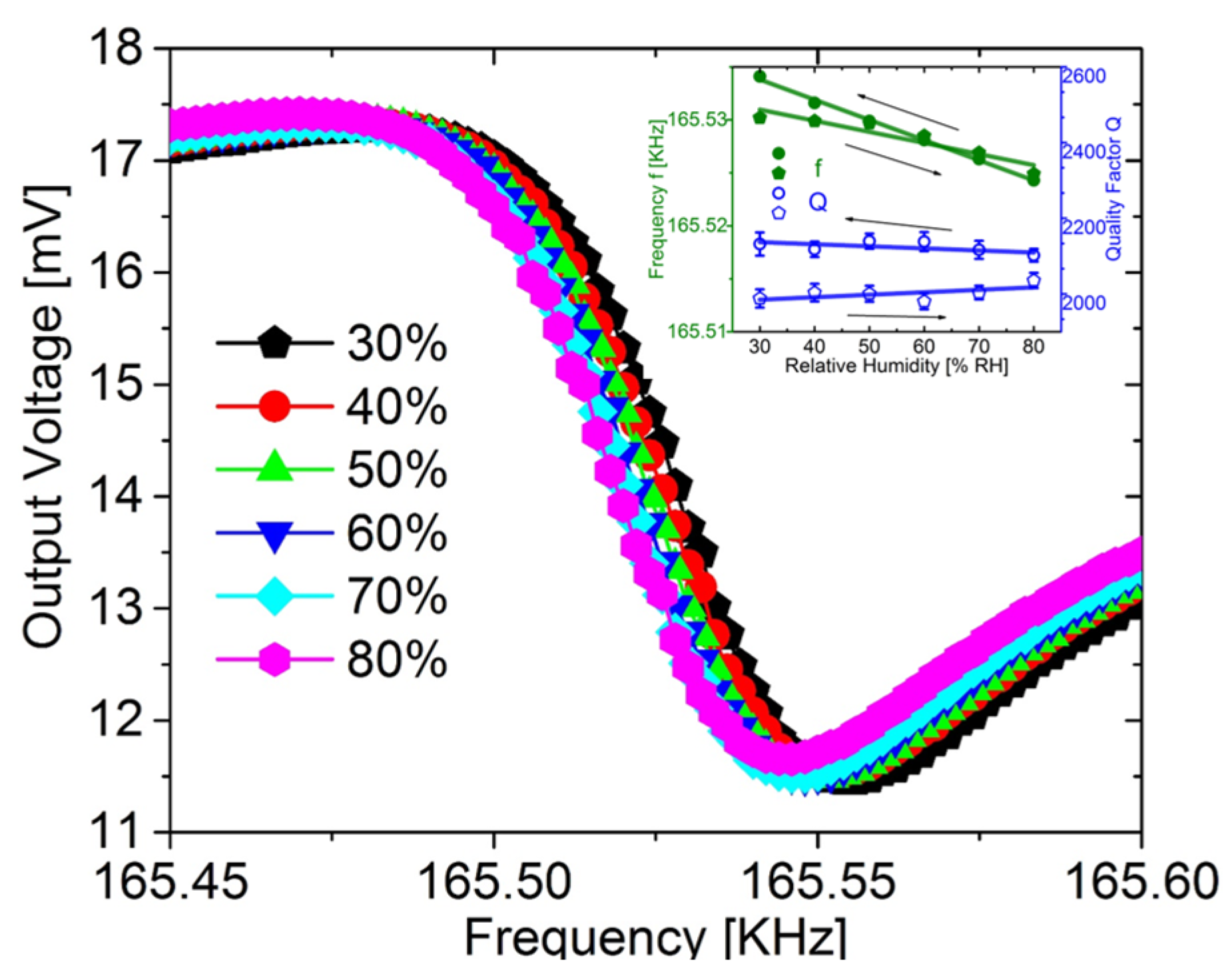
2.2. Characterization
3. Results and Discussion
4. Conclusions
Acknowledgments
Conflicts of Interest
References
- Zhu, D.; Fu, Y.; Zang, W.; Zhao, Y.; Xing, L.; Xue, X. Piezo/Active Humidity Sensing of CeO2/ZnO and SnO2/ZnO Nanoarray Nanogenerators with High Response and Large Detecting Range. Sens. Actuators B Chem. 2014, 205, 12–19. [Google Scholar] [CrossRef]
- Wagner, A.; Bakin, A.; Otto, T.; Zimmermann, M.; Jahn, B.; Waag, A. Fabrication and Characterization of Nanoporous ZnO Layers for Sensing Applications. Thin Solid Films 2012, 520, 4662–4665. [Google Scholar] [CrossRef]
- Bakin, A.; Behrends, A.; Wagner, A.; Waag, A. Zinc Oxide Nanostructures. In Fabrication of ZnO Nanostructures; Pan Stanford Publishing Pte Ltd.: Singapore, 2014; ISBN 978-981-4411-33-2. [Google Scholar]
- Kilinc, N.; Cakmak, O.; Kosemen, A.; Ermek, E.; Ozturk, S. Fabrication of 1D ZnO nanostructures on MEMS cantilever for VOC sensor application. Sens. Actuators B Chem. 2014, 202, 357–364. [Google Scholar] [CrossRef]
- Yang, J.; Xu, J.; Wu, W.; Bertke, M.; Wasisto, H.S.; Peiner, E. Piezoresistive silicon cantilever covered by ZnO nanorods for humidity sensing. Proc. Eng. 2016, 168, 1114–1117. [Google Scholar] [CrossRef]
- Bertke, M.; Hamdana, G.; Wu, W.; Wasisto, H.S.; Uhde, E.; Peiner, E. Analysis of asymmetric resonance response of thermally excited silicon micro-cantilevers for mass-sensitive nanoparticle detection. J. Micromech. Microeng. 2017, 27, 064001. [Google Scholar] [CrossRef]
- Asar, N.; Erol, A.; Okur, S.; Arikan, M.C. Morphology-dependent humidity adsorption kinetics of ZnO nanostructures. Sens. Actuators B 2012, 187, 37–42. [Google Scholar] [CrossRef]
- Sakly, N.; Said, A.H.; Ouada, H.B. Humidity-sensing properties of ZnO QDs coated QCM: Optimization, modeling and kinetic investigations. Mater. Sci. Semicond. Process. 2014, 27, 130–139. [Google Scholar] [CrossRef]


| Seedlayer Type | Diameter/nm | Length/nm | Area Density/μm−2 |
|---|---|---|---|
| Without seedlayer | 195 ± 45 | 2203 ± 225 | 2.7 ± 0.8 |
| CBD seedlayer | 115 ± 26 | 995 ± 98 | 26 ± 1 |
| Sputter coating seedlayer | 144 ± 24 | 1348 ± 39 | 38 ± 2 |
Publisher’s Note: MDPI stays neutral with regard to jurisdictional claims in published maps and institutional affiliations. |
© 2017 by the authors. Licensee MDPI, Basel, Switzerland. This article is an open access article distributed under the terms and conditions of the Creative Commons Attribution (CC BY) license (https://creativecommons.org/licenses/by/4.0/).
Share and Cite
Xu, J.; Bertke, M.; Gad, A.; Yu, F.; Hamdana, G.; Bakin, A.; Peiner, E. Fabrication of ZnO Nanorods on MEMS Piezoresistive Silicon Microcantilevers for Environmental Monitoring. Proceedings 2017, 1, 290. https://doi.org/10.3390/proceedings1040290
Xu J, Bertke M, Gad A, Yu F, Hamdana G, Bakin A, Peiner E. Fabrication of ZnO Nanorods on MEMS Piezoresistive Silicon Microcantilevers for Environmental Monitoring. Proceedings. 2017; 1(4):290. https://doi.org/10.3390/proceedings1040290
Chicago/Turabian StyleXu, Jiushuai, Maik Bertke, Alaaeldin Gad, Feng Yu, Gerry Hamdana, Andrey Bakin, and Erwin Peiner. 2017. "Fabrication of ZnO Nanorods on MEMS Piezoresistive Silicon Microcantilevers for Environmental Monitoring" Proceedings 1, no. 4: 290. https://doi.org/10.3390/proceedings1040290