Low-Power Heating Platform for the Characterization and Calibration of Scanning Thermal Probes †

1
EPFL-LMTS, Neuchatel, Switzerland
2
FEMTO-ST, MN2S, 25000 Besançon, France
*
Author to whom correspondence should be addressed.
†
Presented at the Eurosensors 2017 Conference, Paris, France, 3–6 September 2017.
Proceedings 2017, 1(4), 334; https://doi.org/10.3390/proceedings1040334
Published: 25 August 2017
(This article belongs to the Proceedings of Proceedings of Eurosensors 2017, Paris, France, 3–6 September 2017)
Abstract
:We report on a micro-hotplate technology platform optimized for the calibration of Scanning Thermal Microscopy probes (SThM) used in surface temperature measurement mode. The three chips designed include the same heating area with a calibration area of 10 × 10 µm2 where the SThM probes can land. The 1st design allows to study the influence of the nature of the material on the SThM probes thermal contact resistance. The 2nd design includes a resistive temperature sensor (RTD) integrated on the contact area, which is dedicated to evaluate the capability of a probe to measure a surface temperature. The 3rd design has a contact area made of a suspended platinum membrane for coupling SThM probes with optical thermal measurements. The thermal response of a thermocouple (TC) SThM probe was extracted demonstrating the relevance of these chips for SThM probes characterization and calibration.
1. Introduction
Scanning Thermal Microscopy has become a major tool for investigating heat transport of materials at very low scale. Derived from Atomic Force Microscopes, they are able to operate in two complementary modes, either in passive mode for surface temperature measurements [1], or in active mode for thermal parameters estimation (thermal conductivity or diffusivity typically) [2]. However, none of these modes are reliable yet due to the complexity of the thermal interaction between the probe tip and a sample surface. Consequently, calibration procedures and adapted tools still have to be demonstrated before considering SThM as quantitative tools. In the frame of the European Union FP7 Project named “QUANTIHEAT”, new tools have been developed in order to monitor and calibrate the SThM probe/surface interactions. In passive mode, active calibration samples are needed to generate a local controlled hot area on which a probe can land. Previous measurements were performed in the past [3] using not adapted hotplates. Recently, a calibration chip design was reported at Eurosensors 2015 conference [4]. We report here on an optimized technology platform including three chips designs for SThM probes characterization and calibration. The designs developed in this work exhibit low-power consumption and uniform circular temperature distribution over the SThM contact area. The minimization of the power consumption is crucial for increasing the thermal sensitivity. By an appropriate combination of the platinum and silicon nitride layers, the three calibration chips designs can be realized in the same fabrication run.
2. Design and Fabrication
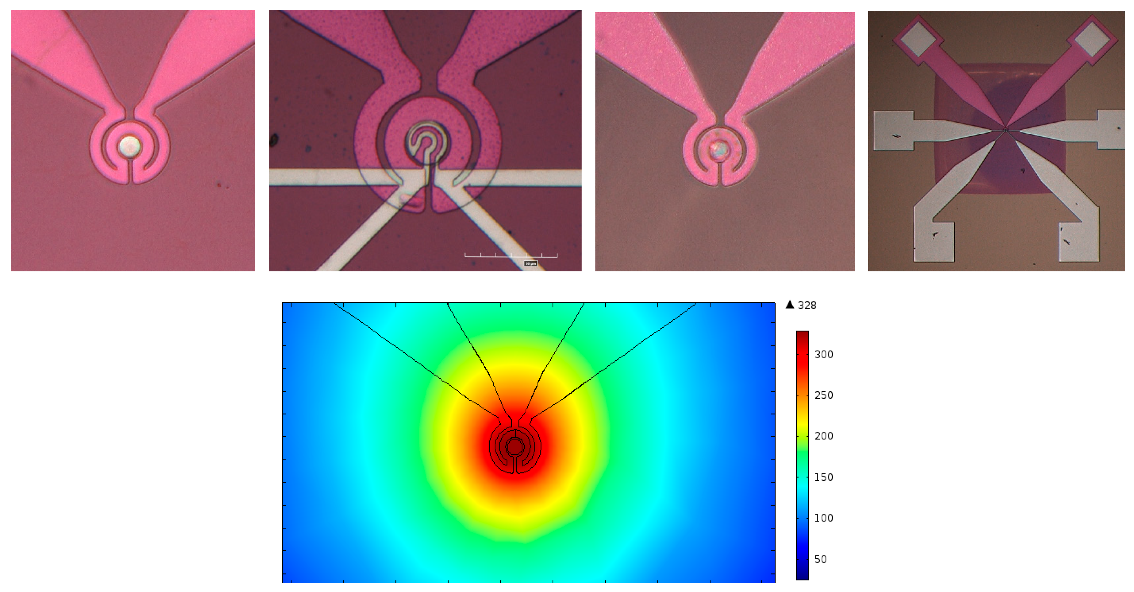
The calibration chips are made of a platinum heater, with an area of 50 × 50 µm2 sandwiched in a suspended silicon nitride membrane, and a SThM contact area of 10 × 10 µm2, as shown in Figure 1.
On top of the heating area and centered, the 1st design includes a pad of material of different nature to study its influence on SThM probes thermal contact resistance (here in Pt). The 2nd design has a RTD patterned locally and centered on top of the heating area. The RTD provides the actual surface contact temperature, which allows monitoring the thermal contact efficiency and the heat flux drained by the SThM probe when in contact with the chip. The 3rd design consists of a suspended circular standalone platinum membrane (150 nm-thick/10 µm-wide) defined in the heater layer. These three designs are depicted in the Figure 2.
3. Results
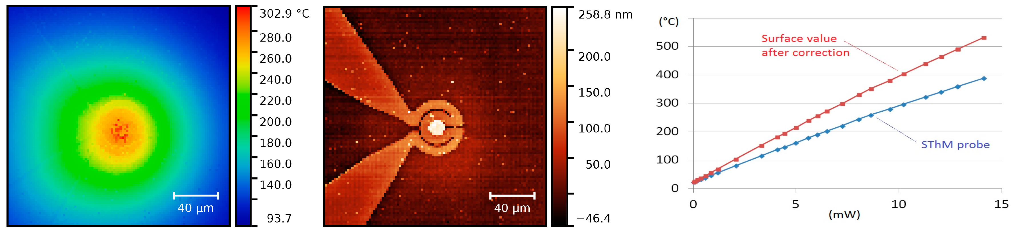
Devices have been electro-thermally characterized by determining the temperature coefficient of the resistors (TCR = 0.00185 K−1) and by measuring temperature vs. power consumption using the SThM thermocouple probe presented in [2]. Figure 3 presents a scan result on the 1st design (temperature and topography maps) at 11 mW power supply and the temperature at the center of the device versus power. Due to imperfect contact and heat sink effect, a contact probe only provides its own temperature which is different from the actual surface temperature [3]. The second design includes a central RTD sensor (four points measurements) in order to quantify this difference, leading to a possible correction as shown in the right plot of Figure 3.
Among the different tested designs, simulations and experiments allowed us to significantly improve our calibration devices. Figure 4 points out the typical influence of a probe contact with two different calibration devices.
Figure 4a,b present the SThM probe scans for topography and temperature obtained on the 2nd design, named Vsmall. Figure 4c shows a comparison made on the central point with respect to a larger version of device (named Vlarge) for which the larger heater (220 × 220 µm2) is shown on the figure (same RTD sensor not plotted). Ts is the RTD surface temperature before contact (Ts nc) and during contact (Ts) of the probe. Tp is the temperature provided by the SThM probe. It clearly shows a large reduction of power consumption and subsequently a greater sensitivity in the measurement of the thermal perturbation, as shown in the zoomed blue area. The mean values of the thermal responses of the SThM probe (see [1,3]) were found to be 0.79 and 0.6 for Vlarge and Vsmall, respectively. Such a factor is one of the most significant parameters that characterize temperature probe efficiency and can be used to correct the measured temperature value. Figure 5 presents the first results obtained on the 3rd design by comparing a SThM measurement scan and a Near Infrared thermograph [5]. The difference between both images clearly shows the influence of the measurement method and confirms the probe thermal response of 0.79. Since SThM provides perturbed surface temperature (uncorrected values), coupling the measurementswith non-contact infrared thermograph will provide a solution to measure the cooling effect induced by the SThM probe in vicinity or in contact with the sample surface.
4. Conclusions
We have developed a series of platforms for operation over a large temperature range, exhibiting low power consumption and high sensitivity. This will open new possibilities to calibrate any local thermal probe. Further tests still have to be performed to confirm the complementarity of these designs.
Acknowledgments
This work has received funding from the European Union Seventh Framework Program FP7-NMP-2013-LARGE-7 under GA No. 604668 Project QUANTIHEAT.
Conflicts of Interest
The authors declare no conflict of interest.
References
- Bontempi, A.; Thiery, L.; Teyssieux, D.; Briand, D.; Vairac, P. Quantitative thermal microscopy using thermoelectric probe in passive mode. Rev. Sci. Instrum. 2013, 84, 103703. [Google Scholar] [CrossRef]
- Bontempi, A.; Nguyen, T.P.; Salut, R.; Thiery, L.; Teyssieux, D.; Vairac, P. Scanning thermal microscopy based on a quartz tuning fork and a microthermocouple in active mode (2ω method). Rev. Sci. Instrum. 2016, 87, 063702. [Google Scholar] [CrossRef]
- Thiery, A.; Toullier, S.; Teyssieux, D.; Briand, D. Thermal contact calibration between a thermocouple probe and a microhotplate. J. Heat Transf. 2008, 130, 091601. [Google Scholar] [CrossRef]
- Lemaire, E.; Nguyen, T.P.; Bontempi, A.; Thiery, L.; Teyssieux, D.; Vairac, P.; Shea, H.; Briand, D. Micromachined calibration chip with heat source and temperature sensors for scanning thermal metrology (SThM). Procedia Eng. 2015, 120, 130–133. [Google Scholar] [CrossRef]
- Teyssieux, D.; Thiery, L.; Cretin, B. Near-infrared thermography using a charge-coupled device camera: Application to microsystems. Rev. Sci. Instrum. 2007, 78, 034902. [Google Scholar] [CrossRef]
Figure 1.
The three calibration chips designs.
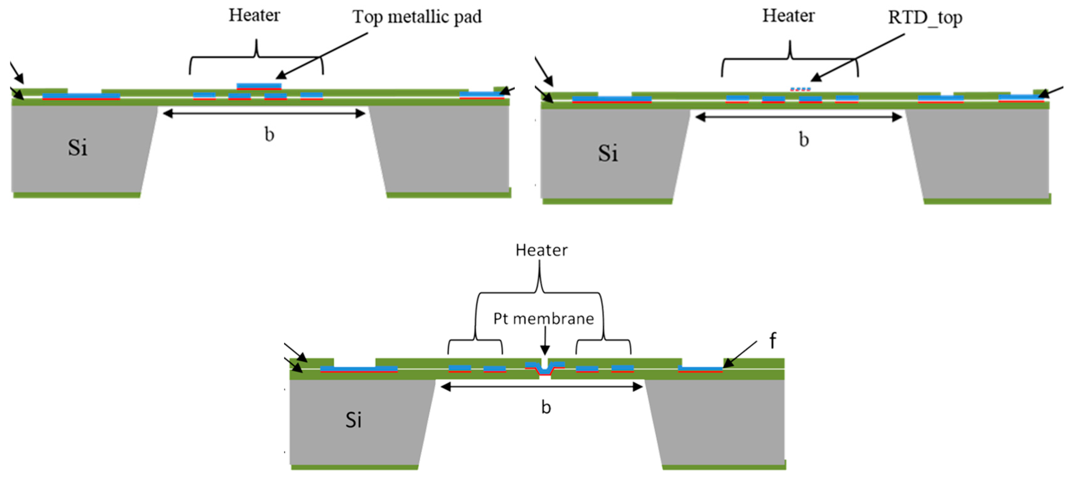
Figure 2.
Calibration chips with heating area of 50 × 50 µm2 and contact area of 10 × 10 um2. Top from left to right: 1st design with metallic pad; 2nd design with Pt RTD; 3rd design with the suspended platinum membrane; full chip. Bottom image: FEM simulation using COMSOL showing homogeneous temperature isotropic distribution on the active area.

Figure 3.
1st Design; (left) surface temperature distribution by SThM; (middle) SThM topography; (right) temperature at the center versus power.
Figure 3.
1st Design; (left) surface temperature distribution by SThM; (middle) SThM topography; (right) temperature at the center versus power.

Figure 4.
2nd Design: (a) SThM TC topography, (b) SThM TC temperature at 1.8 mW, (c) Comparison between TC SThM probe on Vlarge and Vsmall, respectively.
Figure 4.
2nd Design: (a) SThM TC topography, (b) SThM TC temperature at 1.8 mW, (c) Comparison between TC SThM probe on Vlarge and Vsmall, respectively.
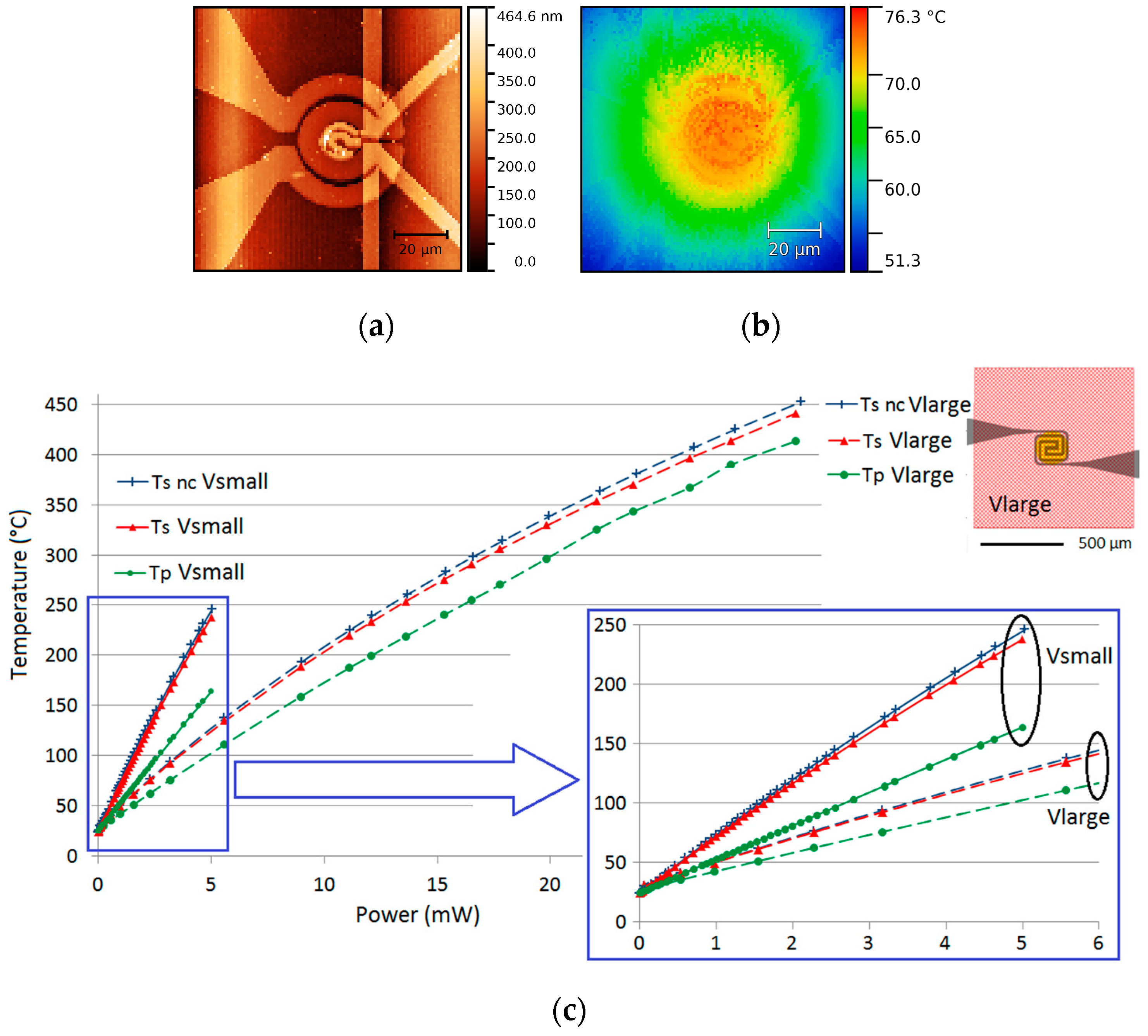
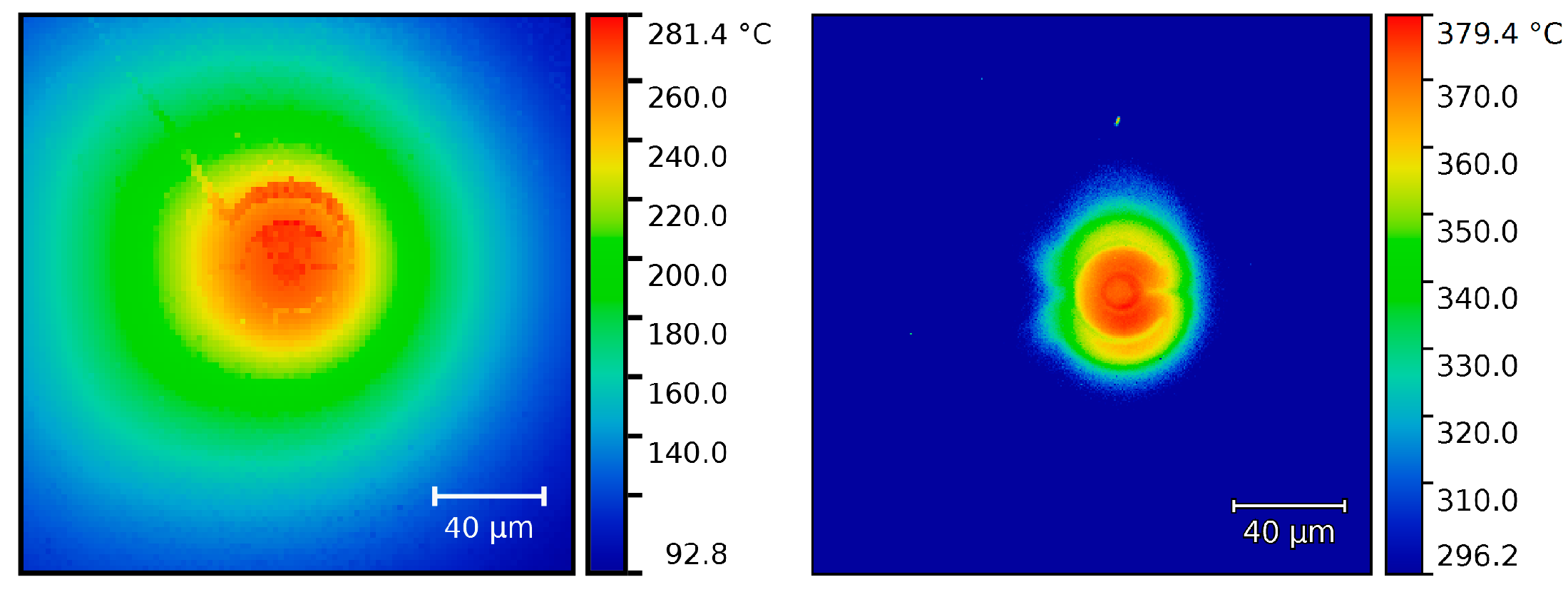
Figure 5.
3rd Design: (left) SThM temperature scan; (left) Near Infrared temperature image at 8.84 mW, before probe contact; (right) NIR temperature subtraction between no contact and contact images.
Figure 5.
3rd Design: (left) SThM temperature scan; (left) Near Infrared temperature image at 8.84 mW, before probe contact; (right) NIR temperature subtraction between no contact and contact images.
© 2017 by the authors. Licensee MDPI, Basel, Switzerland. This article is an open access article distributed under the terms and conditions of the Creative Commons Attribution (CC BY) license (https://creativecommons.org/licenses/by/4.0/).
Share and Cite
MDPI and ACS Style
Briand, D.; Nguyen, T.P.; Lemaire, E.; Thiery, L.; Vairac, P. Low-Power Heating Platform for the Characterization and Calibration of Scanning Thermal Probes. Proceedings 2017, 1, 334. https://doi.org/10.3390/proceedings1040334
AMA Style
Briand D, Nguyen TP, Lemaire E, Thiery L, Vairac P. Low-Power Heating Platform for the Characterization and Calibration of Scanning Thermal Probes. Proceedings. 2017; 1(4):334. https://doi.org/10.3390/proceedings1040334
Chicago/Turabian StyleBriand, Danick, Tran Phong Nguyen, Etienne Lemaire, L. Thiery, and P. Vairac. 2017. "Low-Power Heating Platform for the Characterization and Calibration of Scanning Thermal Probes" Proceedings 1, no. 4: 334. https://doi.org/10.3390/proceedings1040334