A Monolithic Three-Axis Accelerometer with Wafer-Level Package by CMOS MEMS Process †

National Chip Implementation Center, Natioanl Applied Research Laboratories, Taiwan
*
Author to whom correspondence should be addressed.
†
Presented at the Eurosensors 2017 Conference, Paris, France, 3–6 September 2017.
Proceedings 2017, 1(4), 337; https://doi.org/10.3390/proceedings1040337
Published: 11 August 2017
(This article belongs to the Proceedings of Proceedings of Eurosensors 2017, Paris, France, 3–6 September 2017)
Abstract
:This paper presents a monolithic three-axis accelerometer with wafer-level package by CMOS MEMS process. The compositions of the microstructure are selected from CMOS layers in order to suppress the in-plane and out-of-plane bending deflection caused by the residual stresses in multiple layers. A switched-capacitor sensing circuit with a trimming mechanism is used to amplify the capacitive signal, and decrease the output dc offset voltage to ensure the desired output voltage swing. The CMOS MEMS wafer is capped with a silicon wafer using a polymer-based material. The measured sensitivities with and without a wafer-level package range from 113 mV/G to 124 mV/G for the in-plane (x-axis, y-axis) accelerometer, and from 50 mV/G to 53 mV/G for the z-axis accelerometer, respectively.
1. Introduction
Two-chip solutions for MEMS accelerometers have been widely used in commercial inertial sensors [1,2]. The fabrication of the microstructure by surface micromachining with low stress control and high process yields has established a successful model in commercial consumer electronics over the past ten years. However, two-chip solutions usually utilize multiple bonding and packaging processes to integrate the sensor chip and the readout circuit chip, which cost more bond pad or seal-ring area during integration. To save on bonding and packaging, accelerometers based on CMOS MEMS have been proposed to integrate the microstructure and sensing circuit through metal routing or MEMS vias [3,4]. The integration can be categorized based on the use of single-crystalline-silicon (SCS)/polysilicon or multiple compound layers as the microstructure. Microstructures fabricated with SCS/polysilicon have excellent mechanical properties and relatively low stress, corresponding to lower cross-axis effects and excellent performance of sensor’s functionality [5]. Multilayer microstructure such as CMOS MEMS based on foundry-oriented platform is also utilized to fabricate monolithic sensor chip [6]. With this method, the CMOS foundry can conveniently integrate the post-CMOS MEMS process without altering the steps in the standard CMOS process.
This paper proposes a monolithic three-axis accelerometer using a UMC 0.18 μm 1P6M multi-project wafer CMOS MEMS process. Three individual micro-structures are used as in-plane (x-axis, y-axis), and z-axis sensors to reduce sensor size for low structural curling. The circuit topology employs a switched-capacitor integrator to read capacitance changes and uses an auto-trimming technique to cancel the output dc offset voltage. After the CMOS MEMS process, the CMOS MEMS wafer is bonded with a silicon cap using a polymer-based material and then diced out by a stealth laser dicing process [7].
2. Fabrication
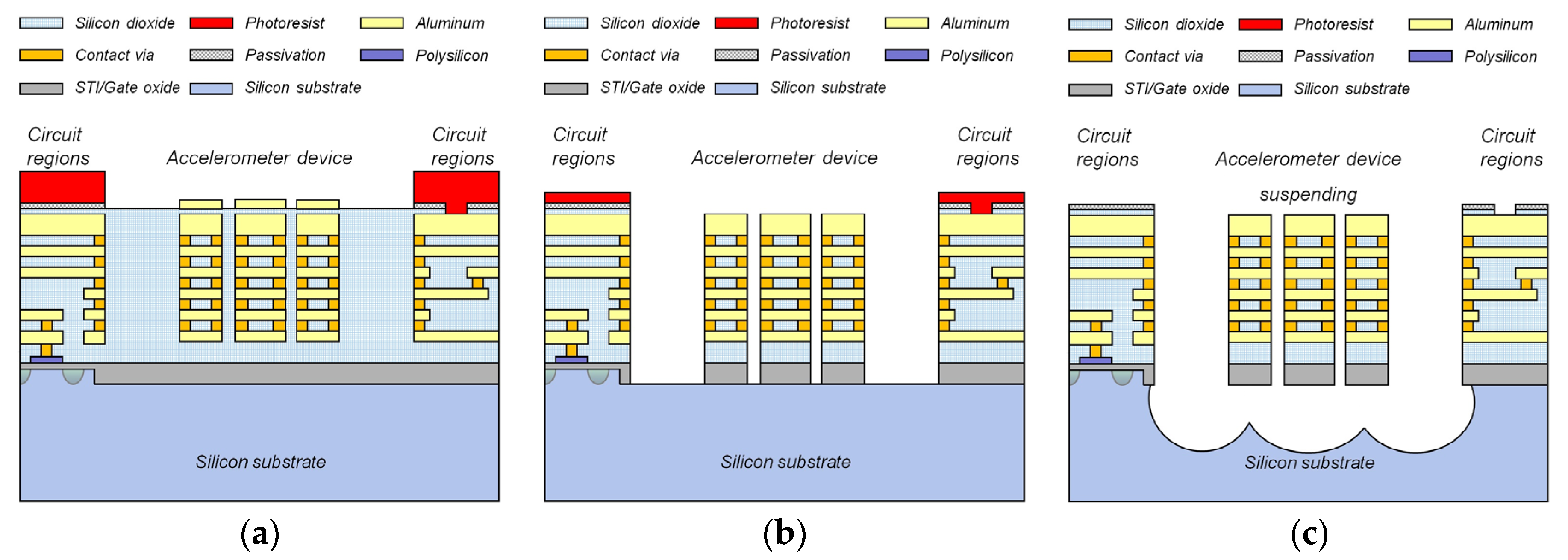
Figure 1 shows the flow of the UMC 0.18 μm 1P6M CMOS process with post-micromachining. The thickness of the microstructure is about 10.3 μm. After the standard CMOS process, a 0.9 μm thick silicon dioxide layer and a 0.8-μm thick aluminum layer are deposited and patterned above the metal-6 layer as the etch-resistant mask, as shown in Figure 1a. The passivation layers are then deposited and patterned except for the mechanical device region. After that, a 12 μm thick photoresist layer is defined above the circuit region for etch protection. The post-micromachining processes are performed using inductively coupled plasma (ICP) dry etching, which is fully compatible with the CMOS process. Figure 1b shows the anisotropic oxide etching between structural sidewalls using CF4 and C4F8. The gap spacing between the microstructure is 2.3 μm. The aluminum masking layer and the silicon dioxide layer above the microstructure are both exhausted in this etching step. Partial photoresist thin films still remain on top of the circuit region as the masking layer for subsequent isotropic release etching of the silicon substrate. After that, the microstructure is released using isotropic silicon undercut etching by SF6, as shown in Figure 1c. The wafer is finally cleaned using O2 plasma to ensure the removal of any residual photoresist thin films. The SEM image in Figure 2a shows the three-axis accelerometer with the sensing circuits. Figure 2b,c show the SEM images of the in-plane and z-axis sensor device, respectively.
3. Design Features
3.1. Micromechanical Resonator
The in-plane accelerometer is supported by four mechanical springs as shown in Figure 2b, where the sensing comb-fingers are attached to the curl-matching frame and the modulation signal is fed into the comb-fingers attached to the proof-mass. Four comb-fingers are employed to provide the electrostatic force for the built-in self-test. The simulated displacement of the sensor device is about 4 nm when the self-test applied voltage is 1.8 V. The shock-stop beam is placed in the middle of the anchor to protect the microstructure from damage due to high shock, where the gap spacing of the shock-stop beam is 2 μm smaller than the gap spacing (2.3 μm) in the sensing comb-fingers. The topology of the z-axis accelerometer uses two torsional beams to connect an asymmetric proof-mass. When an out-of-plane acceleration is applied on the z-axis accelerometer, an unbalanced inertial force causes the proof-mass to rotate slightly. The differential capacitors for in-plane and z-axis accelerometers are made by stacked aluminum and dioxide layers in comb-fingers as shown in Figure 3a,b, respectively. The electrodes of in-plane sensor are composed of the metal-1 to metal-6 layers. When the in-plane sensor is excited by transverse acceleration, differential capacitance changes are produced at V+ and V− according to VS. For the z-axis sensor, the layers of metal-5 to metal-6 act as the upper electrodes and metal-1 to metal-3 layers act as the bottom electrodes. When the sensor is excited in an out-of-plane acceleration, the upper (V+) and bottom (V−) electrodes can sense differential capacitance changes. The capacitance sensitivity of the in-plane and z-axis accelerometers are approximately 1fF/G and 0.52 fF/G, respectively, based on finite-element simulations [8].
3.2. Circuits
Figure 4 shows the schematic diagram of the switched- capacitor sensing circuit with the trimming diagram. Each axis has three non-overlapped clock signals CLKa, CLKb, CLKr, which are used for charge resetting, dc bias setting, signal sensing, and low frequency noise cancellation. The first stage is primarily used for the capacitance to voltage converter, and the gain is about 2∆C/Cint, where Cint is the feedback capacitor of the amplifier (~200 fF), ∆C is the sensing capacitance change. Generally, the dc offset voltage appears at the circuit output due to mismatches from process variations in the integrated capacitor and mismatches between the sensing capacitors between comb-fingers. The offset voltage may deteriorate the output dynamic range, and in the worst cases, the output signal may be saturated if the dc offset voltage is too large.
The offset voltage from the amplifier can be solved by using correlated double sampling to remove unwanted errors. Other techniques such as capacitor trimming and circuit calibration may be considered to remove offset voltage from the sensor device. Capacitor trimming usually relies on using a series of capacitors to compensate for different output voltages. This requires extra chip area to incorporate a number of capacitors. In this work, an external 8-bit trimming pattern is added into a digital to analog converter (DAC), which generates a compensated voltage. This voltage is then applied to another input pair of the amplifier which induces a reverse offset current added to the input node of the pre-amp. These steps are repeated until the pre-amp’s output offset voltage is smaller than 50 mV. The final stage is a programmable gain amplifier (PGA) which provides the extra gain for the output voltages of the three-axis accelerometers.
4. Experimental Results
The maximum structural curling of the in-plane and z-axis accelerometers with selected layers is controlled to remain under 0.2 μm and 4.6 μm, respectively. Figure 5 shows the self-test result of the accelerometer, where a 1.8 V square-wave with 20 Hz was fed into built-in self-test comb-fingers to provide the electrostatic force, corresponding to the output amplitude of about 119 mV. The sensitivities of the three-axis accelerometer with and without capping were measured between 0–6 G in Figure 6, where the nonlinearity is under 1%. The sensitivities of the three-axis accelerometer with and without the capping process are approximate, where they range from 113 mV/G to 124 mV/G for the in-plane accelerometer and from 50-mV/G to 53 mV/G for the z-axis accelerometer, respectively. The dissimilarities are possibly duep to process variations from structural thickness (about 10% mismatch) and the etching processes for different chips. In this work, a polymer-based bonding material was used for wafer level packaging. The bonding width is about 75 μm, and the spacing gap between bonded wafers is about 10-μm after bonding. Since the microstructure is composed of CMOS layers, the maximum baking temperature during the bonding process is controlled to be less than 220 °C. The individual CMOS MEMS chip with a cap was diced by stealth laser dicing after wafer bonding. Figure 7a shows the image of two monolithic three-axis CMOS MEMS accelerometers, where the left one is with a silicon cap and the right one is diced without a capping process. Figure 7b shows the SEM image of the cross-sectional view of the CMOS MEMS chip with a silicon cap.
5. Conclusions
This paper presents a monolithic three-axis accelerometer fabricated using a UMC 0.18 μm CMOS MEMS process. A switched-capacitor circuit with a trimming solution is used to decrease the output offset voltage. The mechanisms of self-test and shock-stop are both implemented in the sensor to meet the requirement for consumer electronics. A wafer-level package based on a polymer-based material is employed to achieve chip integration without other technique such as chip stacking. Including the process mismatch, variations in sensor sensitivity changes are under 10%, which shows that this packaging process is practical for the integration of the CMOS MEMS process.
Acknowledgments
The authors would like to thank the National Chip Implementation (CIC) and UMC Ltd., Taiwan, for financial support and chip fabrication.
Conflicts of Interest
The authors declare no conflict of interest.
References
- Vigna, B. MEMS epiphany. In Proceedings of the IEEE MEMS 2009, Sorrento, Italy, 26–29 January 2009; pp. 1–6. [Google Scholar]
- Marek, J. MEMS for automotive and consumer electronics. In Proceedings of the 2010 IEEE International Solid-State Circuits Conference, Francisco, CA, USA, 7–11 February 2010; pp. 9–17. [Google Scholar]
- Chua, S.L.; Razzaq, A.; Wee, K.H.; Li, K.H.; Yu, H.; Tan, C.S. 3D CMOS-MEMS stacking with TSV-less and face-to-face direct metal bonding. In Proceedings of the IEEE Symposium on VSLI Technology, Honolulu, HI, USA, 9–12 June 2014. [Google Scholar]
- Zhu, W.; Zhang, Y.; Meng, G.; Wallace, C.S.; Yazdi, N. A CMOS-integrated four-quadrant symmetric micro-g accelerometer. In Proceedings of the IEEE MEMS, Shanghai, China, 24–28 January 2016; pp. 926–929. [Google Scholar]
- Funk, K.; Emmerich, H.; Schilp, A.; Offenberg, M.; Neul, R.; Larmer, F. A surface micromachined silicon gyroscope using thick polysilicon layer. In Proceedings of the IEEE MEMS 1999, Orlando, FL, USA, 17–21 January 1999; pp. 57–60. [Google Scholar]
- Tseng, S.H.; Lu, M.S.C.; Wu, P.C.; Teng, Y.C.; Tsai, H.H.; Juang, Y.Z. Implementation of a monolithic capacitive accelerometer in a wafer-level 0.18 μm CMOS MEMS process. J. Micromech. Microeng. 2012, 22, 055010. [Google Scholar] [CrossRef]
- Klug, G. Advanced solutions for ultra-thin wafers and packaging. In Proceedings of the IEEE European Microelectronics and Packaging Conference (EMPC), Rimini, Italy, 16–18 June 2009; pp. 1–4. [Google Scholar]
- Coventor Inc. 2014. CoSolveEM Toolbox Rev. A.
Figure 1.
Steps of the CMOS MEMS process: (a) the aluminum hard mask and thick photoresist layer after completion of the standard CMOS process; (b) anisotropic dry silicon dioxide etching, and (c) isotropic dry silicon etching and structural release.
Figure 1.
Steps of the CMOS MEMS process: (a) the aluminum hard mask and thick photoresist layer after completion of the standard CMOS process; (b) anisotropic dry silicon dioxide etching, and (c) isotropic dry silicon etching and structural release.

Figure 2.
(a) SEM image of the monolithic CMOS MEMS three-axis accelerometer; (b) SEM image of in-plane (x-axis or y-axis) sensor, and (c) SEM image of z-axis sensor.
Figure 2.
(a) SEM image of the monolithic CMOS MEMS three-axis accelerometer; (b) SEM image of in-plane (x-axis or y-axis) sensor, and (c) SEM image of z-axis sensor.
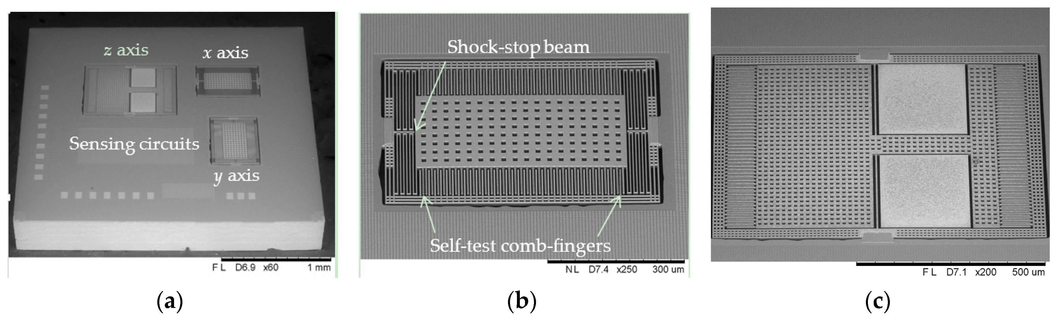
Figure 3.
CMOS stacked layers for differential electrodes (a) in-plane, and (b) z-axis accelerometer.
Figure 3.
CMOS stacked layers for differential electrodes (a) in-plane, and (b) z-axis accelerometer.

Figure 4.
Schematic diagram of the switched-capacitor sensing circuit with trimming diagram.
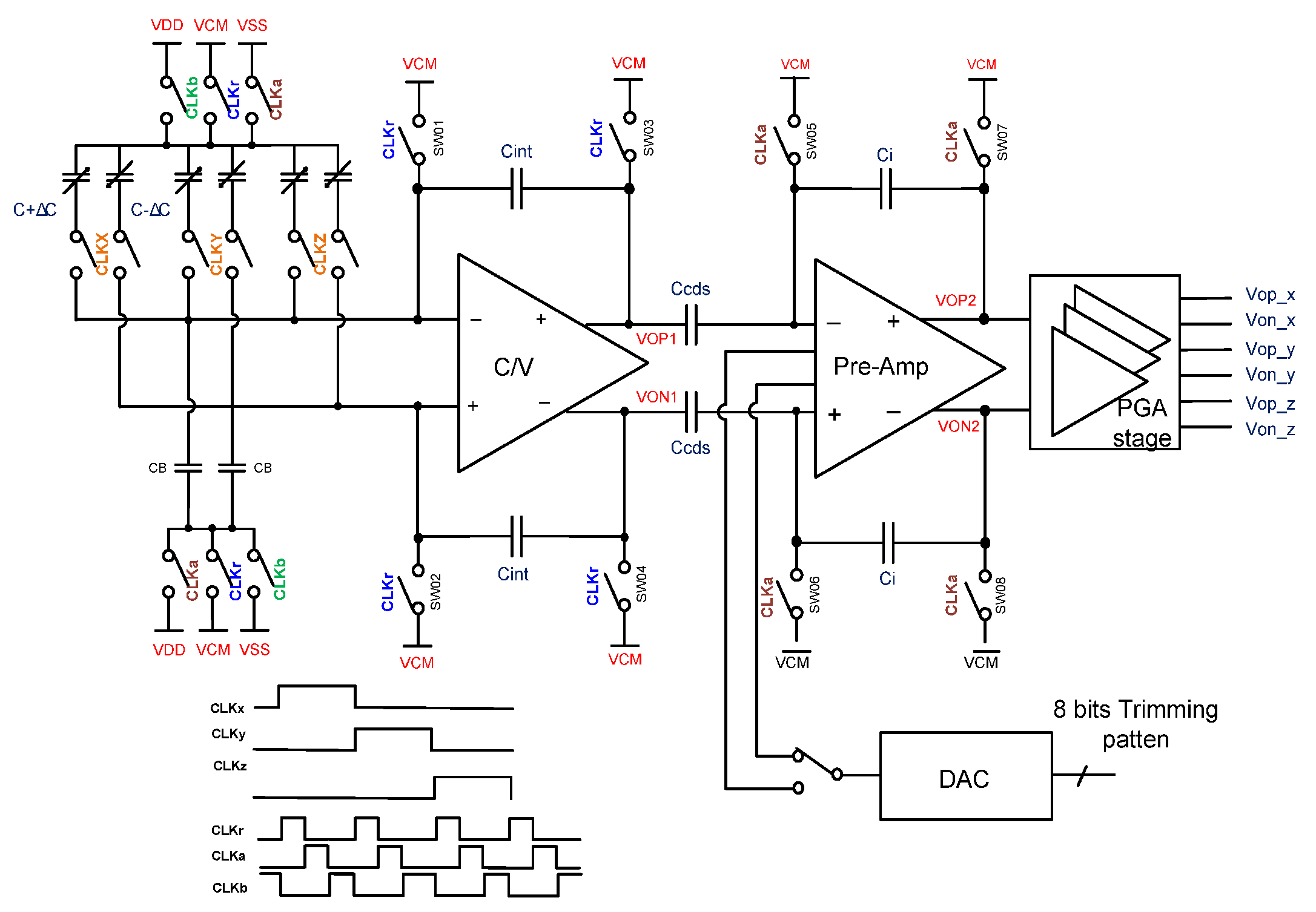
Figure 5.
Output waveforms excited by 1.8 V self-test voltage with 20 Hz.
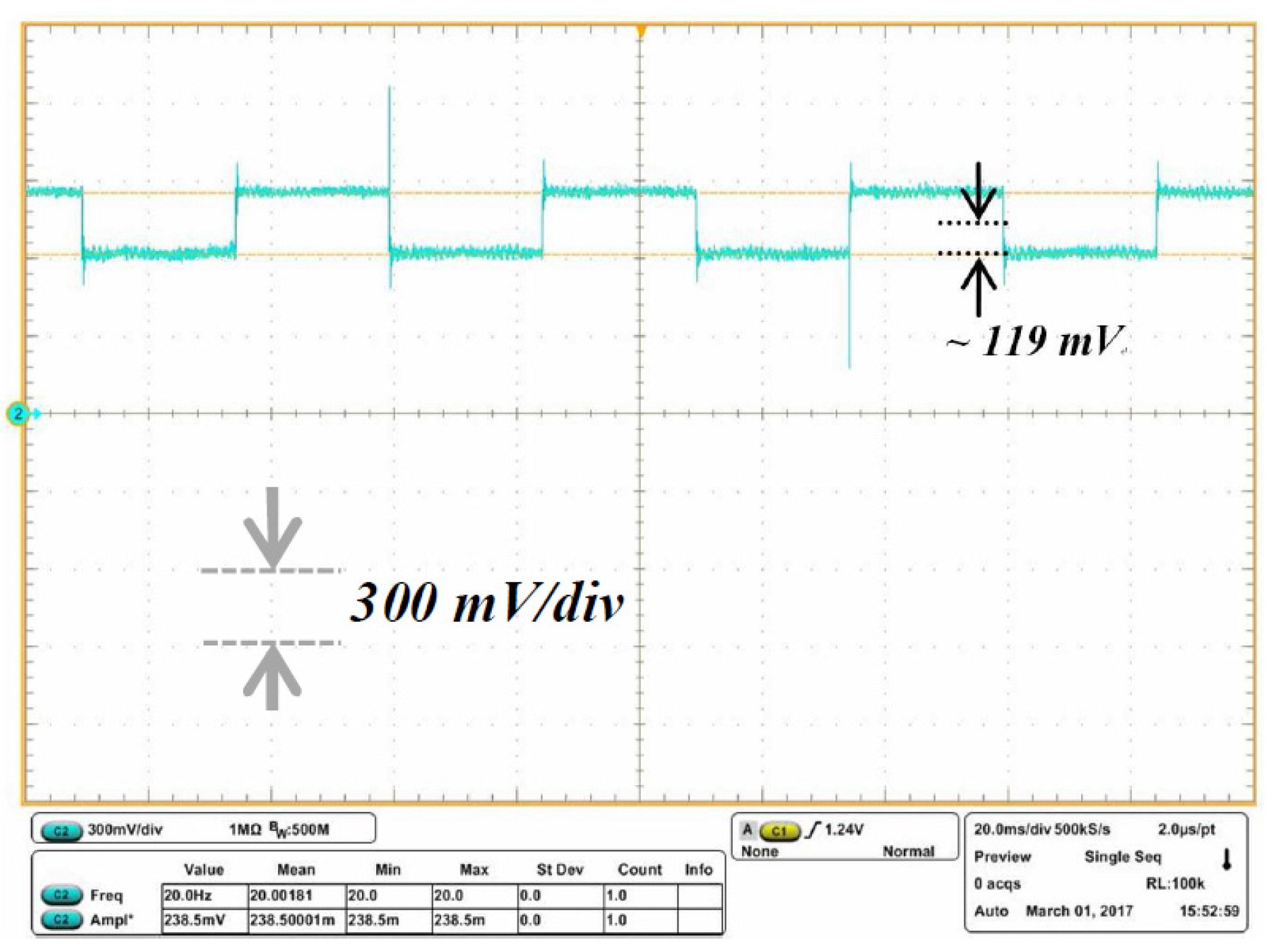
Figure 6.
Voltage output sensitivities of three-axis CMOS MEMS accelerometer with/without capping.
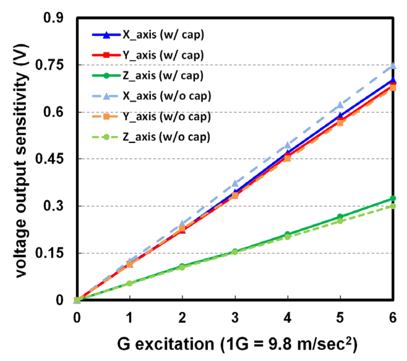
Figure 7.
(a) Monolithic three-axis CMOS MEMS accelerometer with/without cap packaging; (b) SEM of cross-sectional view of silicon cap and chip.
Figure 7.
(a) Monolithic three-axis CMOS MEMS accelerometer with/without cap packaging; (b) SEM of cross-sectional view of silicon cap and chip.

Publisher’s Note: MDPI stays neutral with regard to jurisdictional claims in published maps and institutional affiliations. |
© 2017 by the authors. Licensee MDPI, Basel, Switzerland. This article is an open access article distributed under the terms and conditions of the Creative Commons Attribution (CC BY) license (https://creativecommons.org/licenses/by/4.0/).
Share and Cite
MDPI and ACS Style
Tseng, S.H.; Yeh, C.Y.; Chang, A.Y.; Wang, Y.J.; Chen, P.C.; Tsai, H.H.; Juang, Y.Z. A Monolithic Three-Axis Accelerometer with Wafer-Level Package by CMOS MEMS Process. Proceedings 2017, 1, 337. https://doi.org/10.3390/proceedings1040337
AMA Style
Tseng SH, Yeh CY, Chang AY, Wang YJ, Chen PC, Tsai HH, Juang YZ. A Monolithic Three-Axis Accelerometer with Wafer-Level Package by CMOS MEMS Process. Proceedings. 2017; 1(4):337. https://doi.org/10.3390/proceedings1040337
Chicago/Turabian StyleTseng, S. H., C. Y. Yeh, A. Y. Chang, Y. J. Wang, P. C. Chen, H. H. Tsai, and Y. Z. Juang. 2017. "A Monolithic Three-Axis Accelerometer with Wafer-Level Package by CMOS MEMS Process" Proceedings 1, no. 4: 337. https://doi.org/10.3390/proceedings1040337