Linear-Logarithmic CMOS Image Sensor with Reduced FPN Using Photogate and Cascode MOSFET †
by
Myunghan Bae
1, 
Byung-Soo Choi
1,
Sang-Hwan Kim
1,
Jimin Lee
1,
Chang-Woo Oh
2,
Pyung Choi
1 and
Jang-Kyoo Shin
1,* 1
School of Electronics Engineering, Kyungpook National University, Daegu 41566, Korea
2
Department of Sensor and Display Engineering, Kyungpook National University, Daegu 41566, Korea
*
Author to whom correspondence should be addressed.
†
Presented at the Eurosensors 2017 Conference, Paris, France, 3–6 September 2017.
Proceedings 2017, 1(4), 338; https://doi.org/10.3390/proceedings1040338
Published: 18 August 2017
(This article belongs to the Proceedings of Proceedings of Eurosensors 2017, Paris, France, 3–6 September 2017)
Abstract
:We propose a linear-logarithmic CMOS image sensor with reduced fixed pattern noise (FPN). The proposed linear-logarithmic pixel based on a conventional 3-transistor active pixel sensor (APS) structure has additional circuits in which a photogate and a cascade MOSFET are integrated with the pixel structure in conjunction with the photodiode. To improve FPN, we applied the PMOSFET hard reset method as a reset transistor instead of NMOSFET reset normally used in APS. The proposed pixel has been designed and fabricated using 0.18-μm 1-poly 6-metal standard CMOS process. A 120 × 240 pixel array of test chip was divided into 2 different subsections with 60 × 240 sub-arrays, so that the proposed linear-logarithmic pixel with reduced FPN could be compared with the conventional linear-logarithmic pixel. We confirmed a reduction of pixel response variation which affected image quality.
1. Introduction
Real-world scenes have dynamic intra-scene ranges that might extend about seven orders or more of magnitude, from 10−2 lux in the shadows to 105 lux in the bright sunlight [1]. Unfortunately, charged coupled devices (CCDs) image sensors and complementary metal-oxide semiconductor (CMOS) image sensors (CISs), which currently dominate the image sensor market, have a dynamic range of less than four orders of magnitude. Consequently, when imaging natural and industrial scenes, the response of these sensors is to saturate parts of the scene. To overcome these problems, several on-chip techniques have been proposed that can extend the dynamic range of image sensors. Several approaches have been proposed to extend the dynamic range of an image sensor [2,3,4,5,6,7,8,9]. Logarithmic pixel can achieve a dynamic range above 100 dB. However, logarithmic pixel lead to a poor output swing. The multiple sampling technique provides wide dynamic range without pixel modification. However, the conventional multiple sampling method requires additional frame memories and an image synthesis process. Overflow integration capacitor method is not appropriate for small pixels due to their in-pixel lateral capacitor.
We proposed a new CMOS image sensor that extends the dynamic range using a photogate and a cascode MOSFET. The proposed linear-logarithmic CMOS image sensor successfully extended the dynamic range and perfectly worked as expected [10,11]. However, there is also a negative effect due to the added parts for extending the dynamic range. It is not serious to limit the size of the pixel or the size of the photodiode area. Their mismatch lead to variations in the image sensor’s output. This variation can be removed by using correlated double sampling (CDS) circuits or double sampling (DS) circuits. Before applying the CDS and the DS, we tried to find out how to reduce the variation at the pixel level.
2. Pixel Structure
The conventional linear-logarithmic pixel is proposed for wide dynamic range CMOS image sensors. The pixel based on a three-transistor active pixel sensor has two linear responses and a logarithmic response using a photogate and a cascode MOSFET. We propose a new linear-logarithmic pixel for a FPN reduction by slightly changing the structure of the previously proposed pixel. The MOSFET transfers the voltage using a soft reset and a hard reset. Generally, the soft reset method is mainly used. However, this method causes an offset level due to the influence of the threshold voltage mismatch. The hard reset can completely eliminate the influence of the threshold voltage [8]. The NMOSFET hard reset requires an additional larger voltage source than the power supply voltage. Thus, the PMOSFET hard reset that does not require an additional power source is applied to proposed pixel for FPN reduction. The proposed pixel was designed to evaluate the proposed method for FPN reduction. Figure 1 shows the schematic diagrams of the conventional linear-logarithmic pixel and the proposed linear-logarithmic pixel to reduce the pixel response variation using the PMOSFET hard reset.
3. Experimental Results
The pixels have been designed using 0.18-μm 1-poly 6-metal standard CMOS process. A 120 × 240 pixel array of test chip was divided into 2 different subsections with 60 × 240 sub-arrays, so that the proposed linear-logarithmic pixel with reduced FPN could be compared with the conventional linear-logarithmic pixel.
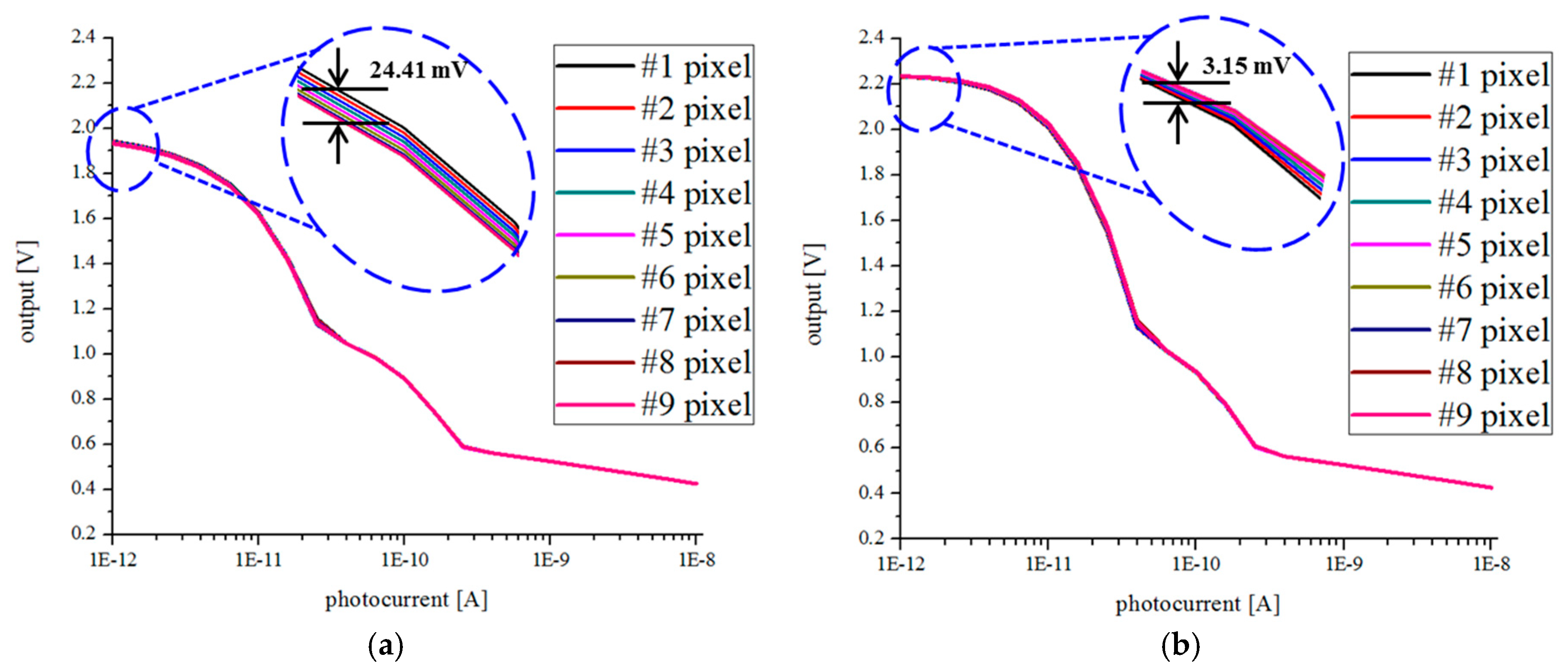
Figure 2 shows simulation results of the conventional linear-logarithmic pixel’s output curves and proposed linear-logarithmic pixel’s output curves according to the reset method. The conventional pixel using NMOSFET reset exhibits a rather wide range of variation in the first linear response region, whereas the proposed pixel using PMOSFET reset exhibits a relatively narrow range of variation. It indicates that the pixel responses are mostly uniform. That is, the FPN of proposed pixel is smaller than the conventional pixel.
Based on these simulation results, the image sensor was designed as a sub-array using the conventional linear-logarithmic pixel and the proposed linear-logarithmic pixel for a comparison. The image sensor for FPN reduction in the first linear response was designed in a 240 × 120 array with the conventional linear-logarithmic pixel in a 240 × 60 sub-array and the proposed linear-logarithmic pixel in a 240 × 60 sub-array. Figure 3 shows the output image of the image sensor. The image of the proposed linear-logarithmic pixel appears more uniform in the logarithmic response region as shown Figure 3. The reduction effect of the pixel response variation was pronounced.
4. Conclusions
We propose a linear-logarithmic CMOS image sensor with reduced FPN using the PMOSFET hard reset. The proposed image sensor has been designed and fabricated using 0.18-μm 1-poly 6-metal standard CMOS process. A test chip was divided into 2 different subsections with sub-arrays, so that the proposed linear-logarithmic pixel with reduced FPN could be compared with the conventional linear-logarithmic pixel. The proposed linear-logarithmic pixel exhibited a reduction of pixel response variation in the first linear region.
Acknowledgments
This work was supported by Samsung Electronics Co., Ltd., BK21 Plus project funded by the Ministry of Education, Korea (21A20131600011), and the Integrated Circuit Design Education Center (IDEC) in Korea.
Conflicts of Interest
The authors declare no conflict of interest.
References
- Theuwissen, A.J.P. Better pictures through physics. IEEE Solid-State Circuits Mag. 2010, 2, 22–28. [Google Scholar] [CrossRef]
- Graf, H.-G.; Harendt, C.; Engelhardt, T.; Scherjon, C.; Warkentin, K.; Richter, H.; Burghartz, J.N. High dynamic range CMOS imager technologies for biomedical applications. IEEE J. Solid-State Circuits 2009, 44, 281–288. [Google Scholar] [CrossRef]
- Mabuchi, K.; Nakamura, N.; Funatsu, E.; Abe, T.; Umeda, T.; Hoshino, T.; Suzuki, R.; Sumi, H. CMOS image sensors comprised of floating diffusion driving pixels with buried photodiode. IEEE J. Solid-State Circuit 2004, 39, 2408–2416. [Google Scholar] [CrossRef]
- Cheng, H.; Choubey, B.; Collins, S. An integrating wide dynamic range image sensor with a logarithmic response. IEEE Trans. Electron Devices 2009, 56, 2423–2428. [Google Scholar] [CrossRef]
- Park, D.; Rhee, J.; Joo, Y. Wide dynamic range CMOS image sensor using self-reset technique. IEEE Electron Device Lett. 2007, 28, 890–892. [Google Scholar] [CrossRef]
- Lee, W.; Akahane, N.; Adachi, S.; Mizobuchi, K.; Sugawa, S. A 1.9 e-random noise CMOS image sensor with active feedback operation in each pixel. IEEE Trans. Electron Devices 2009, 56, 2436–2445. [Google Scholar] [CrossRef]
- Hsu, T.H.; Yaung, D.N.; Lin, J.S.; Wuu, S.G.; Chien, H.C.; Tseng, C.H.; Wang, C.S.; Chen, S.F.; Lin, C.Y.; Lin, C.S.; et al. An effective method to improve the sensitivity of deep submicrometer CMOS image sensors. IEEE Electron Device Lett. 2005, 26, 547–549. [Google Scholar] [CrossRef]
- Pain, B.; Yang, G.; Cunningham, T.J.; Wrigley, C.; Hancock, B. An Enhanced-Performance CMOS Imager with a Flushed-Reset Photodiode Pixel. IEEE Trans. Electron Devices 2003, 50, 48–56. [Google Scholar] [CrossRef]
- Chae, Y.; Choe, K.; Kim, B.; Han, G. Sensitivity controllable CMOS image sensor pixel using control gate overlaid on photodiode. IEEE Electron Device Lett. 2007, 28, 495–498. [Google Scholar] [CrossRef]
- Bae, M.; Jo, S.-H.; Choi, B.-S.; Lee, H.H.; Choi, P.; Shin, J.-K. Wide dynamic range linear-logarithmic CMOS image sensor using photogate and cascode MOSFET. Electron. Lett. 2016, 52, 198–200. [Google Scholar] [CrossRef]
- Bae, M.; Choi, B.-S.; Jo, S.-H.; Lee, H.H.; P. Choi, J.-K. A Linear-Logarithmic CMOS Image sensor With Adjustable Dynamic range. IEEE Sens. J. 2016, 16, 5222–5226. [Google Scholar] [CrossRef]
Figure 1.
Schematic diagrams; (a) conventional linear-logarithmic pixel and (b) proposed linear-logarithmic pixel.
Figure 1.
Schematic diagrams; (a) conventional linear-logarithmic pixel and (b) proposed linear-logarithmic pixel.

Figure 2.
Simulation results of output curves according to the reset method; (a) conventional linear-logarithmic pixel and (b) proposed linear-logarithmic pixel.
Figure 2.
Simulation results of output curves according to the reset method; (a) conventional linear-logarithmic pixel and (b) proposed linear-logarithmic pixel.

Figure 3.
Output image of the image sensor.

Publisher’s Note: MDPI stays neutral with regard to jurisdictional claims in published maps and institutional affiliations. |
© 2017 by the authors. Licensee MDPI, Basel, Switzerland. This article is an open access article distributed under the terms and conditions of the Creative Commons Attribution (CC BY) license (https://creativecommons.org/licenses/by/4.0/).
Share and Cite
MDPI and ACS Style
Bae, M.; Choi, B.-S.; Kim, S.-H.; Lee, J.; Oh, C.-W.; Choi, P.; Shin, J.-K. Linear-Logarithmic CMOS Image Sensor with Reduced FPN Using Photogate and Cascode MOSFET. Proceedings 2017, 1, 338. https://doi.org/10.3390/proceedings1040338
AMA Style
Bae M, Choi B-S, Kim S-H, Lee J, Oh C-W, Choi P, Shin J-K. Linear-Logarithmic CMOS Image Sensor with Reduced FPN Using Photogate and Cascode MOSFET. Proceedings. 2017; 1(4):338. https://doi.org/10.3390/proceedings1040338
Chicago/Turabian StyleBae, Myunghan, Byung-Soo Choi, Sang-Hwan Kim, Jimin Lee, Chang-Woo Oh, Pyung Choi, and Jang-Kyoo Shin. 2017. "Linear-Logarithmic CMOS Image Sensor with Reduced FPN Using Photogate and Cascode MOSFET" Proceedings 1, no. 4: 338. https://doi.org/10.3390/proceedings1040338