High Sensitivity Ultraviolet Light Off-Stoichiometric Silicon Oxide-Based Sensors †


Universidad Autónoma de Puebla, Av. San Claudio y 14 Sur. Cp. 72570, Puebla, Mexico
*
Author to whom correspondence should be addressed.
†
Presented at the Eurosensors 2017 Conference, Paris, France, 3–6 September 2017.
Proceedings 2017, 1(4), 382; https://doi.org/10.3390/proceedings1040382
Published: 25 August 2017
(This article belongs to the Proceedings of Proceedings of Eurosensors 2017, Paris, France, 3–6 September 2017)
Abstract
:We have developed a UV silicon detector made of silicon and off-stoichiometric silicon dioxide that shows high efficiency and is completely compatible with silicon devices technology. The silicon-based UV detector present a solar cell-like structure which does not require any voltage source. In addition, an off-stoichiometric silicon dioxide film (Silicon Rich Oxide) with silicon nanocrystals has been integrated to this structure. It is shown that the spectral response is due to the high photoluminescence of Si nanocrystals in the visible region when illuminated with UV light and an increase of 100% in the UV detector efficiency is observed with respect to conventional silicon dioxide layers.
1. Introduction
Many potential applications exist for sensitive UV detectors, which has led to increase the interest in developing Si-based UV sensors because the technology is mature and cheaper than others. It is possible to extend the sensitivity of silicon in the UV region, by integrating an off-stoichiometry silicon dioxide layer with silicon nanocrystals. Many different techniques have been reported to get silicon nanocrystals, however, Chemical Vapor Deposition (CVD) is a very simple method to obtain a good control in the size and concentration of silicon nanocrystals. The principle of detection of a p-n silicon photodetector is very similar to that of a p-n silicon solar cell: when irradiated with light, the photons absorbed generate a photocurrent proportional to the incoming radiation. However, the fundamental spectral losses in these devices can be large because of the mismatch between the incident solar spectrum and the spectral absorption properties of the material [1]. One of the aims of this work was to increase the photogenerated current in a UV p-n silicon photodetector by means of off-stoichiometric silicon dioxide (Silicon Rich Oxide) deposited on the photodetector surface. The silicon nanocristals embedded in the Silicon Rich Oxide layer have the optical property of absorption below ~250 nm radiation (UV), so that the absorbed energy by the SRO film is then reemitted as red light (by photoluminescence); in this way the redshift of the short wavelengths offers an increase in the energy conversion efficiency of the silicon photodetector with no significant increase in the cost of fabrication. This work presents all the experimental conditions and results of the UV silicon photodetector using a silicon rich oxide to increase the sensitivity.
2. Experimental Conditions
The SRO films were deposited on (100) p-type CZ silicon wafers with 3–5 Ohm-cm resistivity. The wafers were cleaned by RCA 1 and RCA 2 standard cleaning process prior to deposit. The SRO films were deposited using a hot-wall LPCVD (Low pressure CVD) furnace at 725 °C using silane and nitrous oxide as reactive gases; the flow ratio (Ro) between nitrous oxide and silane was used to control the amount of silicon excess into the SRO films; for Ro = 30 (SRO30), the silicon excess is of 4.5% according to previous work [2], and for the SRO films with Ro = 45 (SRO45), the silicon excess is of 1%, which is similar to a standard silicon oxide deposited by LPCVD. The films were characterized by Photoluminiscence (PL) at room temperature by using a Horiba Jobin Yvon Fluoro-Max3 spectrofluorometer; the films were excited using a light beam of 300 nm, and the luminescence was collected from 350 to 1000 nm. The structure of the photodetector produced is shown in Figure 1.
The experimental process for the UV photodetector fabrication was as follows: before phosphorus diffusion to form the p-n junction, the wafer surface was textured through an anisotropic etching solution with a 30 wt % potassium hydroxide and deionized water during 20 min at 60 °C. This texturing was made with the aim of reducing the losses due to surface reflection. Then the n-type was formed by phosphorus diffusion using phosphine gas source at 900 °C during 30 min. Once the p-n junction was formed, the SRO 30 and 45 SRO films were deposited on the wafer surface of photodetector, as previously mentioned. The UV detectors were characterized with an UV light source in the 250–450 nm range. The current was measured using a 617 Keithly electrometer.
3. Results and Discussion
As shown in previous work [3], the PL intensity of an SRO layer with silicon nanocrystals embedded in the silicon dioxide matrix is related to a better efficiency in the down conversion effect. The PL intensities of the SRO30 films after different annealing treatments are plotted in Figure 2a. All the films exhibit a luminescence band in the 1.43–2.0 eV range. A peak at 1.73 eV was observed in all samples. When the annealing time applied to SRO30 increases, the PL increases as well, as shown in Figure 2. On the other hand, the SRO45 films have very small silicon excess (<1%); in these films the PL was not observed with 20 and 80 min of thermal treatment. After 180 min of thermal treatment a small intensity appears in the films from blue to red regions, as shown in Figure 2b. The above is due to the long thermal treatment, which is enough for the formation of agglomerations of the small silicon excess, creating the defects and silicon clusters that cause the luminescence as explained in [4]. However, the PL intensity of the SRO45 film is practically negligible in order to be used as a photon converter film in a photodetector.
To observe more clearly the influence of the PL on the behavior of the UV silicon photodetector response, in the Table 1 are presented the values of photocurrent and voltage for the detectors fabricated with SRO containing different silicon excesses.
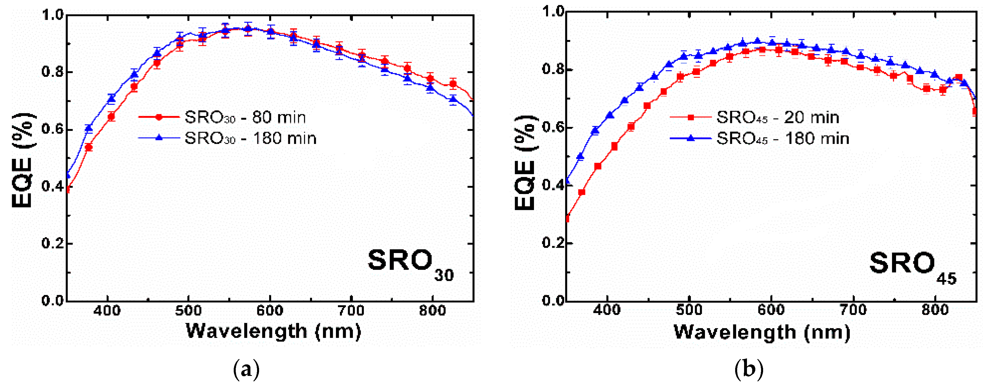
These results clearly show that the SRO-based UV photodetectors present a better response to UV light than the photodetectors covered with conventional silicon dioxide. Several effects could produce the high difference in the values of current and voltage observed. The first effect can result from a very efficient down conversion mechanism from the UV to a longer more easily detectable wavelength (red). In this way all the incident UV radiation can contribute to the SRO emission. To demonstrate this hypothesis, in Figure 3 are shown the External Quantum Efficiency of both kinds of photodetectors, measured in the 350–850 nm range.
The redshift produced by the silicon nanocrystals generates a photocurrent in the SRO30 photodetector which contributes to a higher response, because the emitted light is in the range of the high silicon efficiency. It has also been observed that high photocurrents are obtained when the SRO films are used to produce voltage induced in p-n junction (like in silicon solar cells covered with SRO film). Thus it is possible that SRO contributes in several ways to the photodetector current, so that an extra contribution to the photodetector response has to be considered.
4. Conclusions
A high response of UV detectors using SRO30 with silicon nanocrystals embedded in a silicon dioxide matrix has been observed, compared with a detector using conventional silicon dioxide. It was observed that the PL intensity of the SRO films is related with the response of the photodetector. Also, it was observed that the response of the detector is not affected by a deep junction, so that the annealing temperature to improve the PL intensity is not a significant factor. In addition, the fabrication of the UV detector presented is totally compatible with silicon technology, with a very economic process and easy to implement in a production line.
Acknowledgments
José Alberto Luna collaborated in the fabrication and measurements of the photodetector. Godofredo García participated in the measurements of the EQE of the UV photodetector. Héctor Juárez collaborated in the fabrication of the UV detector. Jesús Carrillo wrote the proceedings. The authors would like to thank Vicerrectoría de Investigación y Estudios de Posgrado (VIEP)-BUAP for providing support for this work. The funds for covering the costs to publish the work will be provided by Instituto de Ciencias-BUAP and VIEP.
Conflicts of Interest
The authors declare no conflict of interest.
References
- Barnham, K.; Marques, J.L.; Hassard, J.; Brien, P.O. Quantum dot concentrator and thermodynamic model for the global redshift. Appl. Phys. Lett. 2000, 76, 1197–1199. [Google Scholar] [CrossRef]
- Morales, A.; Barreto, J.; Domínguez-Horna, C.; Aceves-Mijares, M.; Luna-López, J.A. Optical Characterization of silicon rich oxide films. Sens. Actuators A 2008, 142, 12–18. [Google Scholar] [CrossRef]
- Carrillo-López, J.; Luna-López, J.A.; Vivaldo, I.; Aceves, M.; Morales, A.; García, G. UV enhancement of silicon solar cells using thin SRO films. Sol. Energy Mater. Sol. Cells 2012, 39, 39–42. [Google Scholar] [CrossRef]
- Vivaldo, I.; Carrillo, J.; López, O.; Jiménez, S.; Martínez, J.; Murias, D.; Luna, J.A. Study of the photon down-conversion effect produced by thin silicon-rich oxide films on silicon solar cells. Int. J. Energy Res. 2016. [Google Scholar] [CrossRef]
Figure 1.
Structure of the UV silicon photodetector using an off-stoichiometric silicon oxide layer with silicon nanocrystals embedded in a silicon dioxide matrix.
Figure 1.
Structure of the UV silicon photodetector using an off-stoichiometric silicon oxide layer with silicon nanocrystals embedded in a silicon dioxide matrix.

Figure 2.
(a,b) Photoluminescence spectra of SRO30 and SRO45 films, respectively, for three different annealing times at 1100 °C.
Figure 2.
(a,b) Photoluminescence spectra of SRO30 and SRO45 films, respectively, for three different annealing times at 1100 °C.

Figure 3.
Experimental EQE measured for UV photodetectors covered with SRO30 and SR45 films.


Table 1.
Currents and voltages measured for photodetectors with SRO30 and SRO45 films.
| Photodetector covered with SRO30 | Photodetector covered with SRO45 |
| Current measured 1282 μA and a voltage of 315 mV | Current measured 638 μA and a voltage of 82.6 mV |
© 2017 by the authors. Licensee MDPI, Basel, Switzerland. This article is an open access article distributed under the terms and conditions of the Creative Commons Attribution (CC BY) license (https://creativecommons.org/licenses/by/4.0/).
Share and Cite
MDPI and ACS Style
Carrillo, J.; Luna, J.A.; García, G.; Juárez, H. High Sensitivity Ultraviolet Light Off-Stoichiometric Silicon Oxide-Based Sensors. Proceedings 2017, 1, 382. https://doi.org/10.3390/proceedings1040382
AMA Style
Carrillo J, Luna JA, García G, Juárez H. High Sensitivity Ultraviolet Light Off-Stoichiometric Silicon Oxide-Based Sensors. Proceedings. 2017; 1(4):382. https://doi.org/10.3390/proceedings1040382
Chicago/Turabian StyleCarrillo, Jesús, José Alberto Luna, Godofredo García, and Héctor Juárez. 2017. "High Sensitivity Ultraviolet Light Off-Stoichiometric Silicon Oxide-Based Sensors" Proceedings 1, no. 4: 382. https://doi.org/10.3390/proceedings1040382