1. Introduction
Shape memory alloys (SMA) are materials with various advantages for actuating applications. Their scalability, high work/weight ratio and large stroke, among other properties, account for their suitability for many actuation tasks [
1]. There are, however, challenges regarding their integration in MEMS and the lack of broad experience with this actuation principle. In previous projects, SMA actuators have been used for the actuation of micro-grippers [
2,
3]. The manufacturing process involved manual cold deformation to initialize the actuator and manual assembly of each actuator and gripper. Here we present a novel approach for wafer-level assembly of actuators and grippers by galvanic riveting including femtosecond-laser fabrication of the actuator elements. Using femtosecond-laser pulses minimizes heat transfer into the material, which is of high importance in the case of shape memory alloy micro-actuators [
4].
The micro-grippers to be actuated by the SMA actuators are designed for use in biological applications. Their designated application implies the integration of force-sensitive elements that will be effected by piezoresistive elements. For this reason, silicon has been chosen as the basic gripper material. The activation and control of the actuators will be achieved by resistive heating.
The parameters for the femtosecond-laser fabrication of the shape memory alloy actuators have been studied to avoid thermal damage to the material while obtaining an efficient ablation process. The actuators are cut out of a sheet of NiTi, but after laser-cutting still remain connected in a mesh.
Figure 1 shows the design of the micro-gripper. In panel (a) the silicon gripper structure and the SMA actuator are shown in an exploded view. The spring elements attached to the gripper frame indicated in the figure enable the elongation of the spring-shaped SMA elements after assembly of both parts. This step is necessary, since the actuators are cut out of a sheet of raw material and need to be prestrained before the memory effect can be exploited for gripper actuation, resulting in a contraction of the actuator elements. Both actuator elements, each of them consisting of two parallel SMA springs, are alternately heated by applying a current [
5]. The red arrows in
Figure 1a indicate the electric circuits used to activate the two SMA actuator elements. Panel (b) of
Figure 1 shows the initial deformation of the actuator. Panel (c) of
Figure 1 shows the micro-gripper inserted in a holder that has been designed to enable the prestrain of the actuator elements. The movable part of the gripper frame is shifted outward by a micrometer screw, elongating both silicon and SMA spring elements.
2. Materials and Methods
The shape memory alloy actuators are manufactured from NiTi sheets (54.72 wt-% Ni and 45.25 wt-% Ti) that have been cold formed by milling, annealed and etched by the manufacturer (Memry GmbH Deutschland). The sheet material has a thickness of 70 μm.
The raw SMA material is structured by a femtosecond laser ablation process. The laser used to this end is a frequency-doubled Yb:KGW-solid-state laser (Light Conversion Pharos) with 515 nm wavelength, emitting a beam with a gaussian profile and a diameter of 2.1 mm. The beam is focused on the sample surface using an f-theta lens with a focal length of 100 mm. The spot has an approximate diameter of 25 μm and is positioned on the SMA surface by a galvo-scanner (Scanlab Intelliscan 14/RTC 5) enabling high processing speeds up to 3600 mm/s. The sample is mounted on a micromachining platform (Microstruct-C from 3D-Micromac). The repetition rate was set to 100 kHz for the experiments with a fixed pulse duration of 227 fs.
3. Laser-Cutting of SMA Actuators
In laser micromachining of SMA material, two ablation regimes are described in the literature [
4]. For high precision, a gentle ablation regime with a threshold fluence of 0.16–0.22 J/cm
2, depending on the number of pulses, is recommended. Processes requiring high material removal rates, as is the case for cutting through a 70 μm sheet of SMA, are more efficiently carried out in the strong ablation regime with threshold fluences of 0.75–1.16 J/cm
2.
The parameter sets obtained during the parameter studies for low thermal damage and fast ablation processes are both based on a wavelength of 515 nm, a repetition rate of 100 kHz and a pulse-to-pulse distance of 4 μm. At low pulse energy of 5 μJ, the zone of thermal damage is small, but due to the low ablated material quantities, each contour would have to be repeated approximately 1600 times to cut through the material. The processing time for a wafer-sized batch of SMA actuators fabricated with these parameters is beyond the acceptable range of few hours. At higher pulse energy values of around 65 μJ the thermal damage to the material is more pronounced, but the contour repetitions can be reduced to approximately 125. This strategy is applied for actuator fabrication. With an estimated spot diameter of 25 μm, the fluence values for the two strategies are 1.11 J/cm
2 and 13.24 J/cm
2, respectively. These values are both well in the range of strong ablation according to Uppal et al. [
4]. Deviations in fluence values might in part be due to uncertainties in estimating the spot diameter.
Even though the heat-affected zone is visible at the structure edges, it is limited to few micrometers and has a negligible effect on the shape memory properties of the material. A short wet etching step after laser cutting to remove ridges also diminishes the heat-affected material.
Figure 2 shows images of laser-cut structures before the wet etching.
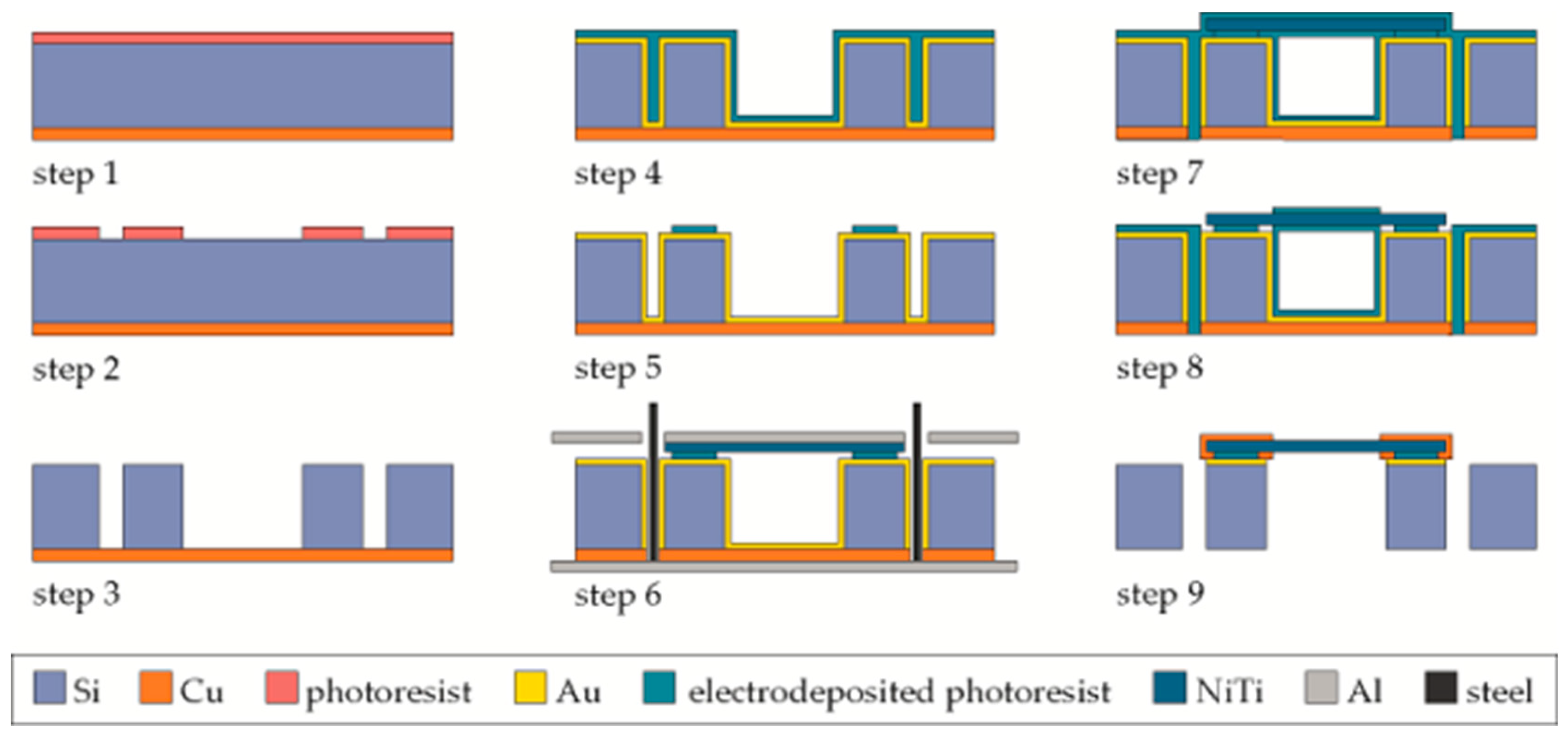
4. Fabrication of Silicon Micro-Grippers and Wafer-Level Assembly of Grippers and Actuators
The fabrication of the micro-grippers and the integration of the actuators at wafer level are illustrated in
Figure 3, the shown steps 1–9 are referenced in the following text.
The backside of a silicon wafer is coated with copper in a physical vapor deposition process (LS 440 S, Ardenne Anlagentechnik). This copper layer has a thickness of approximately 2 μm and serves as a barrier for the reactive-ion etching (RIE) of the silicon and consequently as a stabilization membrane for the wafer, after the micro-gripper outlines have been etched through the entire wafer thickness. The top side of the wafer is spin-coated with photoresist (AZ
® 9260, Microchemicals), which is then photolithographically structured to serve as a mask for the RIE process (steps 1 and 2). The RIE process is carried out in a dry etching unit (STS Multiplex, STS) (step 3). The wafer is consequently sputter-coated with gold and electroplated with a negative 3D photoresist (INTERVIA
TM 3D-N, Dow) (step 4). After photolithography, the remaining photoresist areas serve as adhesive to temporarily fasten the SMA actuators to the silicon wafer (step 5). The laser-cut SMA sheet is sputter-coated with a metallization layer, and both the silicon wafer and the SMA sheet are aligned on an aluminum platform by the use of set pins (step 6). The stack is then loaded with a weight and heated to 60 °C to melt the photoresist. After cooling to room temperature, the wafer and the actuator mesh are temporarily connected and can be coated by another layer of 3D photoresist (step 7), serving as a mask for the subsequent copper electroplating (step 8). A current density of 20 mA/cm
2 is applied for 200 min, yielding a copper layer of approximately 90 μm that connects grippers and actuators by forming a rivet structure. The 3D photoresist is then removed and the copper membrane etched, releasing the single micro-grippers (step 9).
Figure 4 shows microscope pictures of selected intermediate process results.
By means of the silicon element attached to the stiff gripper frame (as shown in
Figure 1a), the initial cold deformation can be carried out after the cleanroom fabrication process is completed. Prior to application in a handling task, each micro-gripper is mounted on a holder for defined positioning and connection to the periphery. Part of the holder fixes the gripper frame, while a second part of the holder allows the defined initial deformation of the SMA actuator (
Figure 1c).
5. Conclusions
The femtosecond-laser ablation of NiTi material has been optimized for the batch fabrication of SMA actuators and different ablation strategies have been studied. A novel wafer-level assembly process for in-plane shape memory alloy actuators and silicon micro-grippers has been developed and tested and first results are shown. The process enables reliable manufacture and in-plane operation of the actuators. A defined prestrain of the actuators is introduced within the process of mounting the grippers to a holder and connecting it to energy supply.

 and
and 


