Low Temperature CVD Grown Graphene for Highly Selective Gas Sensors Working under Ambient Conditions †

 ,
, 
 and
and 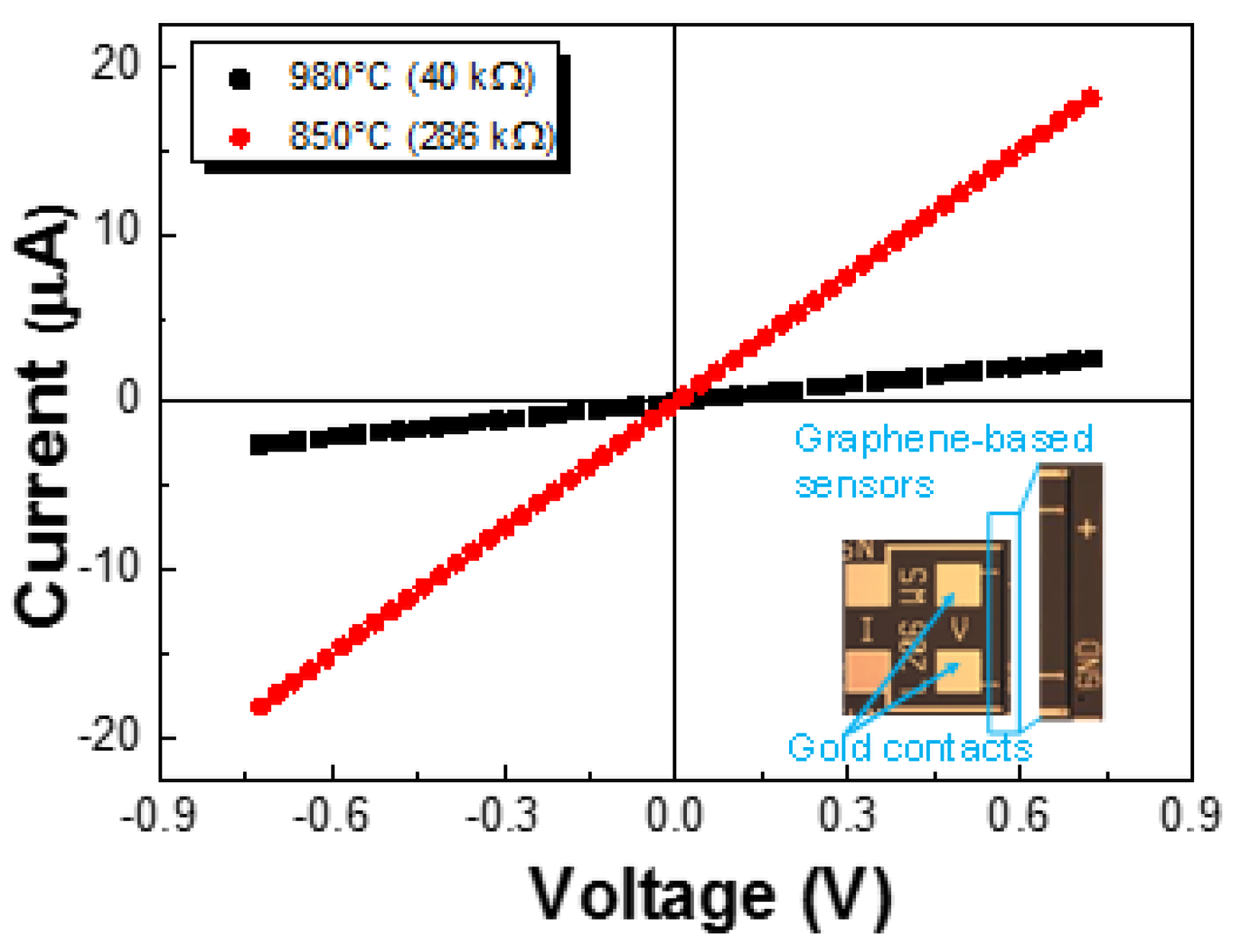
Abstract
:1. Introduction
2. Materials and Methods
2.1. Sensors Preparation
2.2. Sensors Characterization
2.3. Sensors Test-Protocol Description
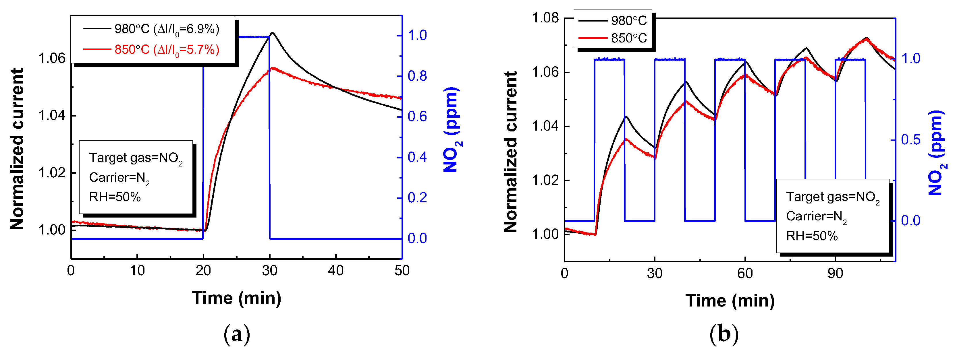
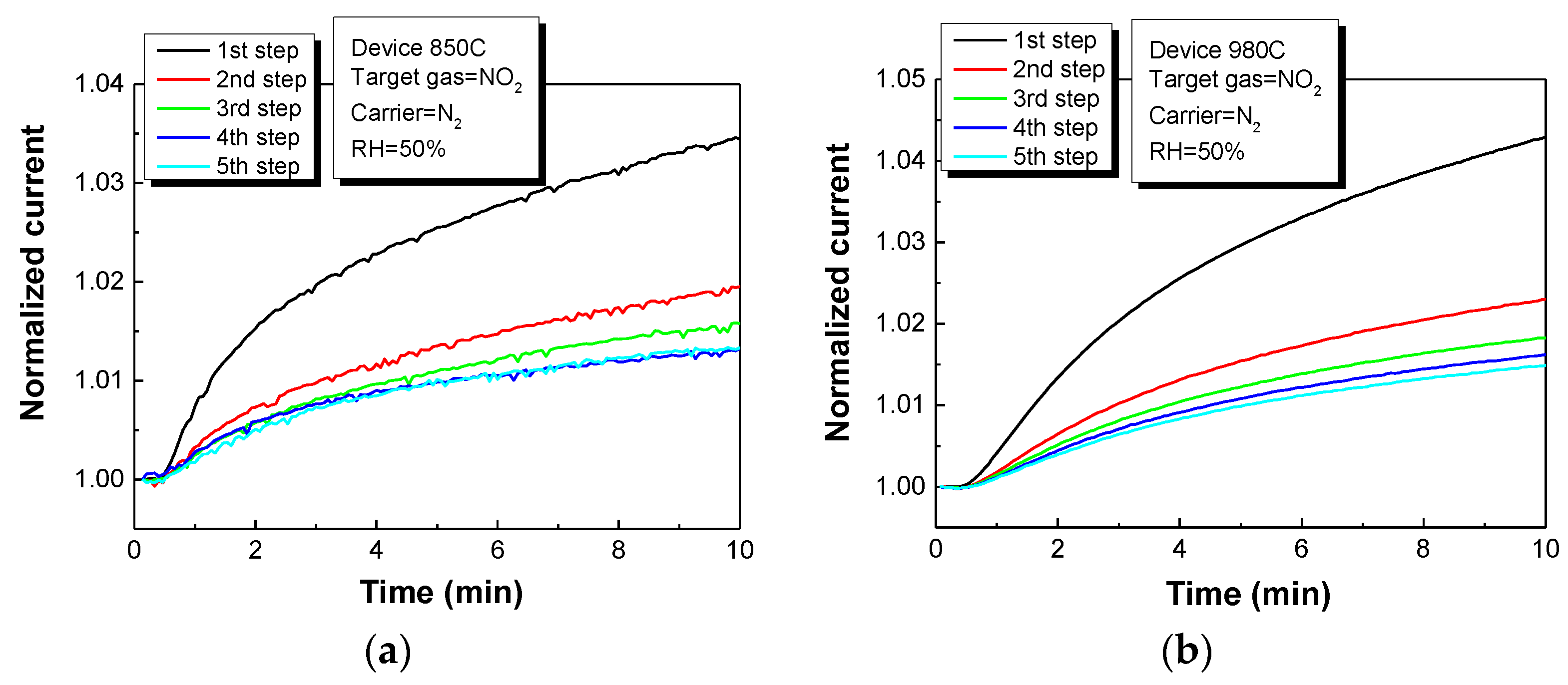
3. Results and Discussion
4. Conclusions
Acknowledgments
Conflicts of Interest
References
- Yuan, W.; Shi, G. Graphene-based gas sensors. J. Mater. Chem. A 2013, 1, 10078–10091. [Google Scholar] [CrossRef]
- Soldano, C.; Mahmood, A.; Dujardin, E. Production, properties and potential of graphene. Carbon 2010, 48, 2127–2150. [Google Scholar] [CrossRef]
- Choi, J.-Y. A stamp for all substrates. Nat. Nanotechnol. 2013, 8, 311–312. [Google Scholar] [CrossRef] [PubMed]
- Ricciardella, F.; Vollebregt, S.; Polichetti, T.; Alfano, B.; Massera, E.; Sarro, P.M. High sensitive gas sensors realized by a transfer-free process of CVD graphene. In Proceedings of the IEEE Sensors, Orlando, FL, USA, 30 October–3 November 2016. [Google Scholar]
- Vollebregt, S.; Alfano, B.; Ricciardella, F.; Giesbers, A.J.M.; Grachova, Y.; van Zeij, H.W.; Polichetti, T.; Sarro, P.M. A transfer-free wafer-scale CVD graphene fabrication process for MEMS/NEMS sensors. In Proceedings of the IEEE MEMS, Shanghai, China, 24–28 January 2016. [Google Scholar]


Publisher’s Note: MDPI stays neutral with regard to jurisdictional claims in published maps and institutional affiliations. |
© 2017 by the authors. Licensee MDPI, Basel, Switzerland. This article is an open access article distributed under the terms and conditions of the Creative Commons Attribution (CC BY) license (https://creativecommons.org/licenses/by/4.0/).
Share and Cite
Ricciardella, F.; Vollebregt, S.; Polichetti, T.; Alfano, B.; Massera, E.; Sarro, P.M. Low Temperature CVD Grown Graphene for Highly Selective Gas Sensors Working under Ambient Conditions. Proceedings 2017, 1, 445. https://doi.org/10.3390/proceedings1040445
Ricciardella F, Vollebregt S, Polichetti T, Alfano B, Massera E, Sarro PM. Low Temperature CVD Grown Graphene for Highly Selective Gas Sensors Working under Ambient Conditions. Proceedings. 2017; 1(4):445. https://doi.org/10.3390/proceedings1040445
Chicago/Turabian StyleRicciardella, Filiberto, Sten Vollebregt, Tiziana Polichetti, Brigida Alfano, Ettore Massera, and Pasqualina M. Sarro. 2017. "Low Temperature CVD Grown Graphene for Highly Selective Gas Sensors Working under Ambient Conditions" Proceedings 1, no. 4: 445. https://doi.org/10.3390/proceedings1040445