Influence of Electrical Modes on Radiation Sensitivity of Hydrogen Sensors Based on Pd-Ta2O5-SiO2-Si Structures †

1
Moscow Engineering Physics Institute, National Research Nuclear University MEPhI, Moscow, Russia
2
Induko Ltd., 32/2 Seslavinskaia str., Moscow, Russia
*
Author to whom correspondence should be addressed.
†
Presented at the Eurosensors 2017 Conference, Paris, France, 3–6 September 2017.
Proceedings 2017, 1(4), 446; https://doi.org/10.3390/proceedings1040446
Published: 25 August 2017
(This article belongs to the Proceedings of Proceedings of Eurosensors 2017, Paris, France, 3–6 September 2017)
Abstract
:The influence of the circuit’s electric modes on the radiation sensitivity of hydrogen sensors based on the metal-insulator-semiconductor field-effect transistor with structure Pd-Ta2O5-SiO2-Si (MISFET) was investigated. There were measured the hydrogen responses of output voltages V of the MISFET-based circuits at different gate voltages before and after the electron irradiations. The voltages V as functions of hydrogen concentration C were determined for different ionizing doses D. Models of influence of the electric modes on the radiation sensitivity of sensors were based on experimental dependencies of V(C, D). The recommendations for the optimal choice of MISFET-based circuit’s electric modes were formulated.
1. Introduction
The hydrogen sensors based on the metal-insulator-semiconductor field-effect transistor (MISFETs) have been studied by many investigators [1,2,3,4,5,6,7]. The studies have shown that the conversion characteristics (the sensor output signals V as function of the hydrogen concentration C) depend on MISFET’s technological parameters [3,5] chip temperature [6] and external factors (other gases, irradiation) [4,7].
This work deals with the integrated hydrogen gas sensors with MISFET sensing element based on Pd-Ta2O5-SiO2-Si structure. The characteristics of these sensors have been already investigated at normal levels of background radiation. However, there are cases, when the gas analysis devices must be used for a long time at raised radiation levels. For examples, in nuclear reactors, in uranium mines, into oil underground deposits search tools based on hydrogen-methane-radon discharge from soil, into the upper atmosphere monitoring systems or into space systems. In spite of low dose rates in above examples, the long-time irradiation (during 200–500 days) may result in degradation of performance characteristics of semiconductor sensors. So the question is: how MISFET-based sensors’ performance characteristics should change under irradiation?
The radiation effects in MIS-structure-based devices are studying since the 1960-ies [7,8,9,10,11,12,13]. It was found the basic radiation effects in MIS structures: increase the concentration of trapping centers under the ionizing radiation, change charges in the dielectrics Qt and on its border with the semiconductor Qss. As a consequence the electrical characteristics of MISFETs are changing. The studies have shown that changes of characteristics depend on temperature, structural-technological characteristics of MISFETs, on total ionizing dose D (TID) and its rate P [9,10,13]. The aim of this work is to investigate the influence of the measuring circuit’s electrical modes on the radiation sensitivity of MISFET-based hydrogen sensors, and to develop models for forecasting the performances of gas-analysis MISFET-based devices under action of ionizing radiation.
2. Materials and Methods
The testing MISFET element based on Pd-Ta2O5-SiO2-Si structure was fabricated on single chip (2 × 2 mm2) together with (p–n)-junction temperature sensor, heater-resistor and Pd-resistor by means of conventional n-MOS-technology using laser evaporation Pd-films. The integrated sensor chip layout with outputs’ pads and the temperature-stabilization circuitry supported chip temperature 130 °C by feedback loop using thermo-sensor and heater are shown in Figure 1.
The parameters of MISFET are the following: acceptors concentration Na = 5 × 1015 cm–3; length L and width z of the channel are 10 µm and 3.2 mm; dielectric capacitance C0 ≈ 30 nF/cm2; transconductance b0 ≈ 2.0 mA/V2. In the first stage of experiments the ID–VG characteristics (VG is the gate voltage) of MISFETs were measured using the measuring system MERA-3 and of circuit No. 1 (Figure 2a; position 2). These characteristics were used to determine the initial values of the threshold voltage VT0, the transconductance b0, the charges in the oxide Qt0 and at SiO2-Si interface Qss0 as in [13]. In the next stages of the experiments before and after the electrons’ irradiations there were measured the hydrogen responses of output voltages V at step-rising concentration C (e.g., Figure 3a) for two types circuits (Figure 2a,b) at different electrical modes, as well as ID–VG characteristics. The sensors were 4 times exposed to electron radiation (6 MeV energy) by the following TID(Si): 50 Gy, 100 Gy, 250 Gy and 850 Gy. The dose rate P(Si) ≈ 2.0 Gy/s.
3. Results Are Presented in Figure 3and Figure 4
4. Discussion
To describe the results there was used the 4-component model of V vs. (C; D) as in [13]:
V (C; D) = V0 (D) − ΔVC (C; D) = V00 − ΔVte (D) + ΔVss(D) − ΔVC (C; D); ΔVte = ΔVteM [1−exp(−k1D)];
ΔVss = ΔVssM [1−exp(−k2D)]; ΔVC (C; D) =ΔVCM [1−exp(−kC)]·{1 − exp[−k3(D3 − D)]}
ΔVss = ΔVssM [1−exp(−k2D)]; ΔVC (C; D) =ΔVCM [1−exp(−kC)]·{1 − exp[−k3(D3 − D)]}
In circuit No. 1 the voltage V is equal to VD, the voltage VG is the controlling parameter:
V = E − 0.5β·(U)2 at 0 < U ≤ Um; V = 1/β + U − [(1/β + U)2 − 2E/β]0.5 at U >Um= [(1 + 2βЕ)0.5 − 1]/β;
U(C; D) = VG − VT0 = VG − VT00 + ΔVC + ΔVte − ΔVss; β = bR.
U(C; D) = VG − VT0 = VG − VT00 + ΔVC + ΔVte − ΔVss; β = bR.
In circuit No. 2 the voltage V is equal to VG, the current ID is the controlling parameter:
V = U(ID) + VT00 − ΔVC − ΔVte + ΔVss; U = {2[ID/b − (φT)2]}0.5, if VD ≥ U; U = ID /(bVD) + 0.5VD, if U > VD
The MISFET’s parameters and the model parameters are presented in [13] and in Table 1. The hydrogen and radiation sensitivities SC(C) = |dV/dC| and SD(D) = |dV/dD| are decreasing in both circuits. Results of experiments and calculations have shown how the conversion functions V(C) and the hydrogen sensitivity SC depend on TID for different gate voltages and drain currents. In circuit No. 1 the sensitivity SC increases with dose’s rising, when MISFET is working in the saturation region of the ID (VD) characteristic (U ≤ Um). Calculated optimum parameters (VG = 1.36 V and R = 3.2 kΩ) correspond to the maximum hydrogen sensitivity SCM ≈ 46 V/% for TID < 850 Gy (Si). In circuit No. 2 the voltage V0 (D) and dose swipe ΔV(D) are increasing with the growth of ID, but the sensitivity SC is not depending on ID.
5. Conclusions
TID effects in the MISFET-based hydrogen sensors depend on electrical modes, which are determined by the type of circuit and its electrical parameters. In circuit No. 1 the conversion characteristics V (C, D) depend on the selected operating voltage VG and value resistor R, which determine the initial value of the output voltage V0 (D) and the hydrogen sensitivity SC. The maximum hydrogen sensitivity SCM is proportional to kβ·ΔVTCM·U(D). So the sensitivity SC is rising with the growth of TID, if parameter U is less than Um. There were determined the optimum parameters VG and R, corresponding to the maximum sensitivity SCM for D < 850 Gy(Si). In circuit No. 2 the initial value of output voltage V0 (D) depends on the current drain ID. With the growth of ID the voltages V0 (D) and the swipe of dose characteristic ΔV(D) are increasing. The sensitivity SC is equal to MISFET’s hydrogen sensitivity |dVT/dC|, which is not depending on ID. Under irradiation doses of D ≤ 700 Gy(Si) the hydrogen sensitivity does not change.
Conflicts of Interest
The authors declare no conflict of interest.
References
- Lundström, I.; Armgarth, M.; Spetz, A.; Winquist, F. Gas sensors based on catalytic metal-gate field-effect devices. Sens. Actuators 1986, 3–4, 399–421. [Google Scholar] [CrossRef]
- Lin, K.-W.; Cheng, C.-C.; Cheng, S.-Y.; Yu, K.H.; Wang, C.-K.; Chuang, H.-M.; Chen, J.Y.; Wu, C.-Z.; Liu, W.-C. A novel Pd/oxide/GaAs metal–insulator–semiconductor field-effect transistor (MISFET) hydrogen sensor. Semicond. Sci. Technol. 2001, 16, 997–1001. [Google Scholar] [CrossRef]
- Lundström, I.; Sundgren, H.; Winquist, F.; Eriksson, M.; Krants-Rülcker, C.; Lloyd-Spets, A. Twenty-five years of field effect gas sensor research in Linköping. Sens. Actuators B 2007, 121, 247–262. [Google Scholar] [CrossRef]
- Kalinina, L.; Litvinov, A.; Nikolaev, I.; Samotaev, N. MIS-Field Effect Sensors for low concentration of H2S for enviromental monitoring. Procedia Eng. 2010, 5, 1216–1219. [Google Scholar] [CrossRef]
- Andersson, M.; Pearce, R.; Lloyd-Spetz, A. New generation SiC based field effect transistor gas sensors. Sens. Actuators B 2013, 179, 95–106. [Google Scholar] [CrossRef]
- Podlepetsky, B.I.; Nikiforova, M.Y.; Kovalenko, A.V. Chip temperature influence on characteristics of MISFET hydrogen sensors. Procedia Eng. 2016, 168, 251–254. [Google Scholar] [CrossRef]
- Podlepetsky, B.I. Effect of irradiation on hydrogen sensors based on MISFET. Sens. Actuators B 2017, 238, 1207–1213. [Google Scholar] [CrossRef]
- Zaininger, K.H. Electron bombardment of MOS capacitors. Appl. Phys. Lett. 1966, 8, 140–144. [Google Scholar] [CrossRef]
- Lenahan, P.M.; Dressendorfer, P.V. Hole traps and trivalent silicon centers in metal/oxide/silicon devices. J. Appl. Phys. 1984, 55, 3495–3499. [Google Scholar] [CrossRef]
- Ionizing Radiation Effects in MOS Devices and Circuits; Ma, T. , Dressendorfer, P., Eds.; Willey & Sons: New York, NY, USA, 1989. [Google Scholar]
- Esqueda, I.S.; Barnaby, H.J.; King, M.P. Compact Modeling of Total Ionizing Dose and Aging Effects in MOS Technologies. IEEE Trans. Nucl. Sci. 2015, 62, 1501–1515. [Google Scholar] [CrossRef]
- Podlepetsky, B.I. Integrated Hydrogen Sensors Based on MIS Transistor Sensitive Elements: Modeling of Characteristics. Autom. Remote Control 2015, 76, 535–547. [Google Scholar] [CrossRef]
- Podlepetsky, B.I. Total Ionizing Dose Effects in Hydrogen Sensors based on MISFET. IEEE Trans. Nucl. Sci. 2016, 63, 2095–2105. [Google Scholar] [CrossRef]
Figure 1.
The temperature-stabilization circuitry, the sensor chip layout with output pads’ and MISFET’s designations: 1—MISFET (G—gate, S—source, D—drain, SB—substrate); 2—heater-resistor (H1–H2); 3—temperature sensor (TS–SB).
Figure 1.
The temperature-stabilization circuitry, the sensor chip layout with output pads’ and MISFET’s designations: 1—MISFET (G—gate, S—source, D—drain, SB—substrate); 2—heater-resistor (H1–H2); 3—temperature sensor (TS–SB).
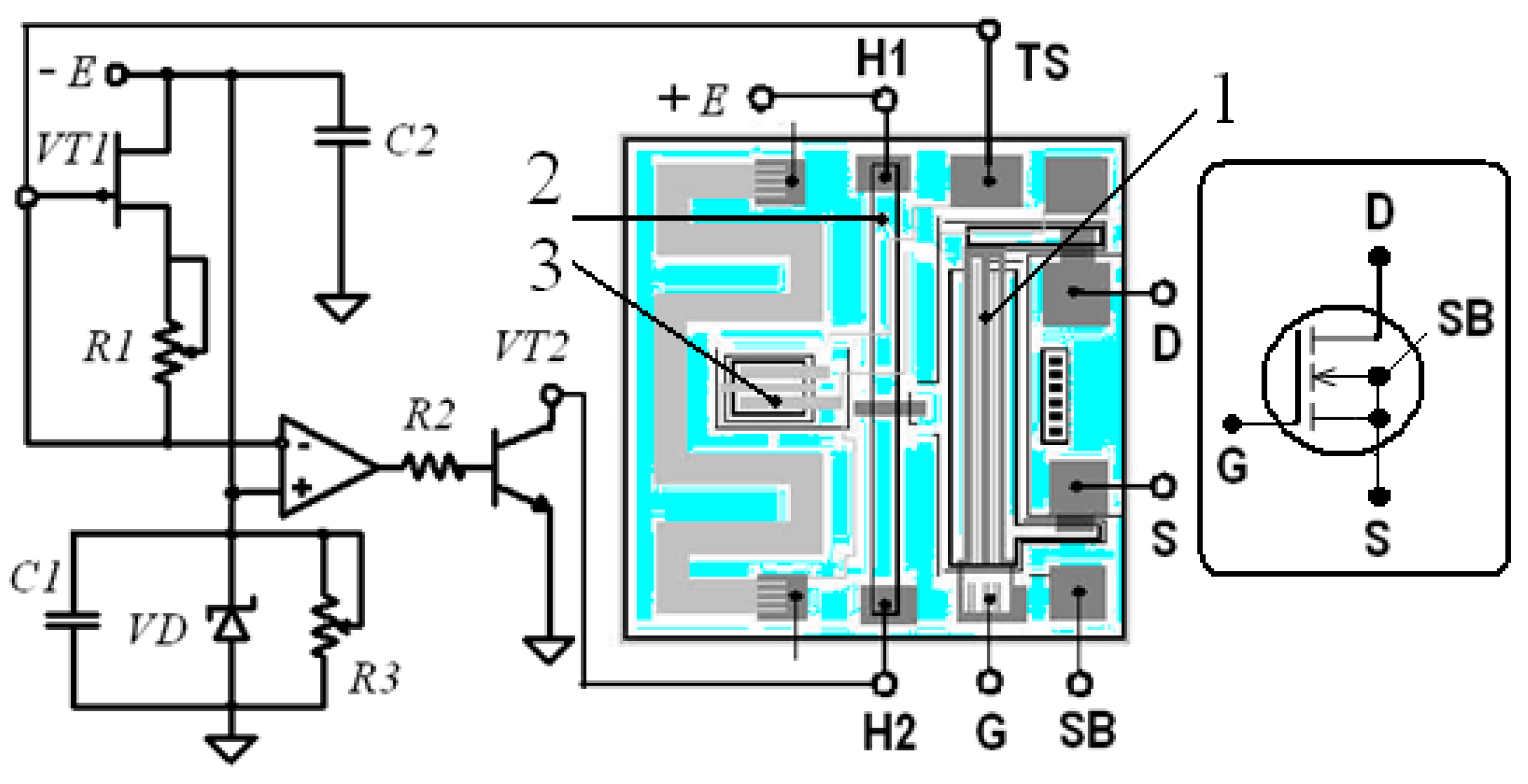
Figure 2.
(a) The circuit No. 1 for measurement the MISFET-based sensors’ conversion functions V(C; D) (position 1) and (ID–VG) characteristics (position 2); (b) The circuit No. 2.
Figure 2.
(a) The circuit No. 1 for measurement the MISFET-based sensors’ conversion functions V(C; D) (position 1) and (ID–VG) characteristics (position 2); (b) The circuit No. 2.
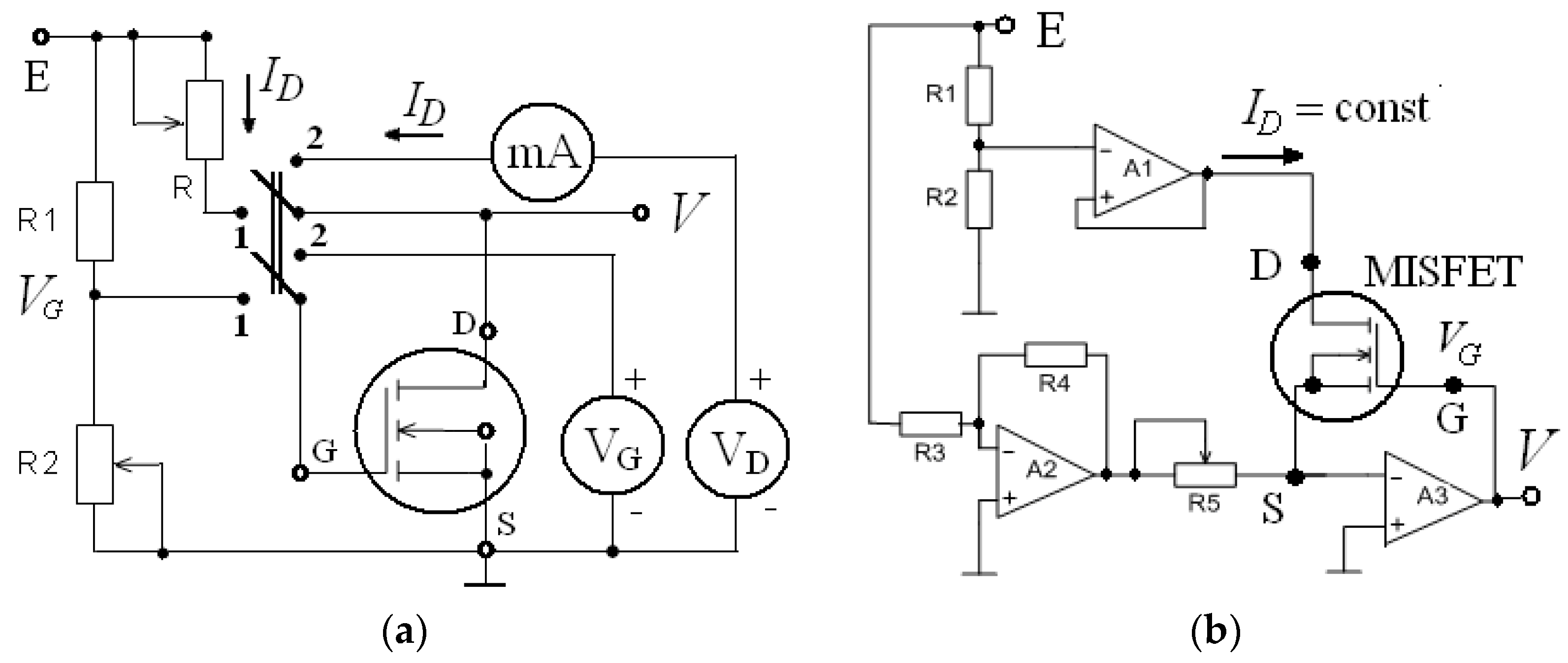
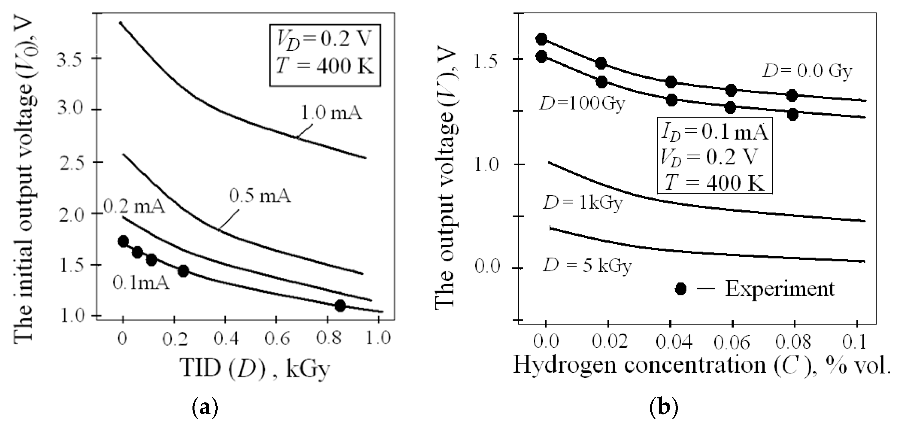
Figure 3.
(a) The hydrogen responses before (1) and after (2) the irradiation by 850 Gy(Si) for circuit No. 1; (b) The output voltages V vs. C at doses D: 0(1); 100 Gy(Si) (2); 250 Gy(Si) (3); 850 Gy(Si) (4) for circuit No. 1.
Figure 3.
(a) The hydrogen responses before (1) and after (2) the irradiation by 850 Gy(Si) for circuit No. 1; (b) The output voltages V vs. C at doses D: 0(1); 100 Gy(Si) (2); 250 Gy(Si) (3); 850 Gy(Si) (4) for circuit No. 1.

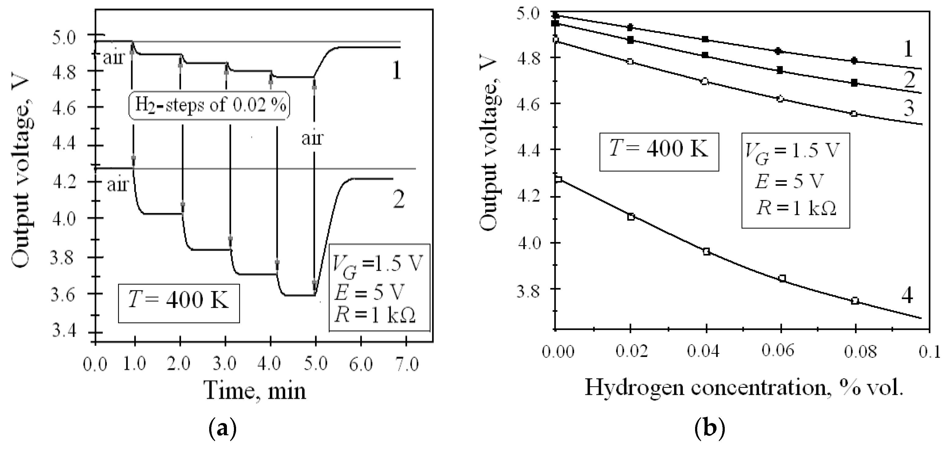
Figure 4.
(a) The initial voltage V0 vs. D at different drain currents for circuit No. 2; (b) The conversion characteristics V vs. C of circuit No. 2 for different TIDs.
Figure 4.
(a) The initial voltage V0 vs. D at different drain currents for circuit No. 2; (b) The conversion characteristics V vs. C of circuit No. 2 for different TIDs.

Table 1.
Average values (dispersion < 10%) of MISFET’s, circuit’s and the model parameters.
| Parameters | VT00, V | b0, mA/V2 | ΔVteM, V | ΔVssM, V | k (1/%) | k1, Gy–1 | k2, Gy–1 | k3, Gy–1 | D3, kGy(Si) |
|---|---|---|---|---|---|---|---|---|---|
| Values | 1.35 | 2.0 | 1.65 | 1.5 | 14 | 6 × 10⁻⁴ | 3 × 10⁻⁵ | 2 × 10⁻⁴ | 15 |
| TID, Gy(Si) | ΔVTCM, V | ∆Vte, V | ∆Vss, V | VT0, V | V0, V | SCM, %/V | b, mA/V2 | ||
| VG = 1.5 V | VG =2 V | VG = 1.5 V | VG = 2 V | ||||||
| 50 | 0.47 | 0.06 | 0.002 | 1.32 | 4.96 | 4.50 | 2.76 | 9.34 | 2.0 |
| 100 | 0.47 | 0.10 | 0.005 | 1.26 | 4.94 | 4.44 | 3.29 | 9.87 | 2.0 |
| 250 | 0.47 | 0.23 | 0.012 | 1.13 | 4.86 | 4.24 | 4.85 | 12.1 | 1.9 |
| 850 | 0.45 | 0.66 | 0.04 | 0.73 | 4.28 | 3.39 | 8.9 | 14.5 | 1.7 |
Publisher’s Note: MDPI stays neutral with regard to jurisdictional claims in published maps and institutional affiliations. |
© 2017 by the authors. Licensee MDPI, Basel, Switzerland. This article is an open access article distributed under the terms and conditions of the Creative Commons Attribution (CC BY) license (https://creativecommons.org/licenses/by/4.0/).
Share and Cite
MDPI and ACS Style
Podlepetsky, B.; Kovalenko, A.; Nikiforova, M. Influence of Electrical Modes on Radiation Sensitivity of Hydrogen Sensors Based on Pd-Ta2O5-SiO2-Si Structures. Proceedings 2017, 1, 446. https://doi.org/10.3390/proceedings1040446
AMA Style
Podlepetsky B, Kovalenko A, Nikiforova M. Influence of Electrical Modes on Radiation Sensitivity of Hydrogen Sensors Based on Pd-Ta2O5-SiO2-Si Structures. Proceedings. 2017; 1(4):446. https://doi.org/10.3390/proceedings1040446
Chicago/Turabian StylePodlepetsky, Boris, Andrew Kovalenko, and Marina Nikiforova. 2017. "Influence of Electrical Modes on Radiation Sensitivity of Hydrogen Sensors Based on Pd-Ta2O5-SiO2-Si Structures" Proceedings 1, no. 4: 446. https://doi.org/10.3390/proceedings1040446