Proceeding Paper

Restraining the Diffusion of Photocarriers to Improve the Spatial Resolution of the Chemical Imaging Sensor †

by
Ko-ichiro Miyamoto
1,*,
Takeyuki Suto
1,
Carl Frederik Werner
1,
Torsten Wagner
2,3,
Michael J. Schöning
2,3 and
Tatsuo Yoshinobu
1
1
Department of Electronic Engineering, Tohoku University, 6-6-05, Aza-Aoba, Aramaki, Aoba-ku, Sendai 980-8579, Japan
2
Institute of Nano- and Biotechnologies, Aachen University of Applied Sciences, Heinrich-Mußmann-Str. 1, Jülich, Germany
3
Peter-Grünberg Institute (PGI-8), Forschungszentrum Jülich GmbH, Leo-Brandt-Str., Jülich, Germany
*
Author to whom correspondence should be addressed.
Presented at the Eurosensors 2017 Conference, Paris, France, 3–6 September 2017.
Proceedings 2017, 1(4), 477; https://doi.org/10.3390/proceedings1040477
Published: 3 August 2017
(This article belongs to the Proceedings of Proceedings of Eurosensors 2017, Paris, France, 3–6 September 2017)

Abstract

:
The chemical imaging sensor is capable of visualizing the ion distribution. The spatial resolution of the chemical image depends on the horizontal diffusion of photocarriers generated by illumination. In this study; a novel optics is designed to realize a hybrid illumination of a ring of constant light and a spot of modulated light. Improved spatial resolution of the order of few tens of microns was successfully demonstrated.

1. Introduction

The chemical imaging sensor [1] is able to visualize the distribution of chemical species by utilizing the principle of a light-addressable potentiometric sensor (LAPS) [2]. As shown in Figure 1a, it has a simple structure consisting of electrolyte—insulator—semiconductor and the amplitude of the photocurrent is recorded during scanning of the sensor plate by a modulated light. Although the chemical imaging sensor can be a powerful tool in analytical chemistry, the problem of relatively low spatial resolution still remains. In the measurement of the chemical imaging sensor, the spatial resolution depends on the horizontal diffusion of photocarriers (Figure 1b).
To overcome the problem, several approaches using thinner silicon substrate have been reported: thinning the wafer by chemical etching [3], using thin-film silicon such as silicon-on-insulator, silicon-on-sapphire [4,5], or amorphous silicon [6]. The improved resolutions of the order of a few microns have been reported in those studies, however, a thinner substrate becomes either mechanically fragile or expensive. Another approach to enhance the spatial resolution is to use a semiconductor material with a shorter diffusion length of minority carriers such as GaAs [7].
In our previous study [8], we demonstrated the enhancement of spatial resolution by a hybrid illumination of a constant light and a modulated light. The additional constant light surrounding the modulated light suppresses the diffusion of photocarriers (Figure 1c), and the spatial resolution can be improved. In the previous study, however, the hybrid illumination was realized by bundled-fibers, which could not precisely define the area of illumination. In this study, we developed a novel optical system for hybrid illumination based on a binocular tube head.

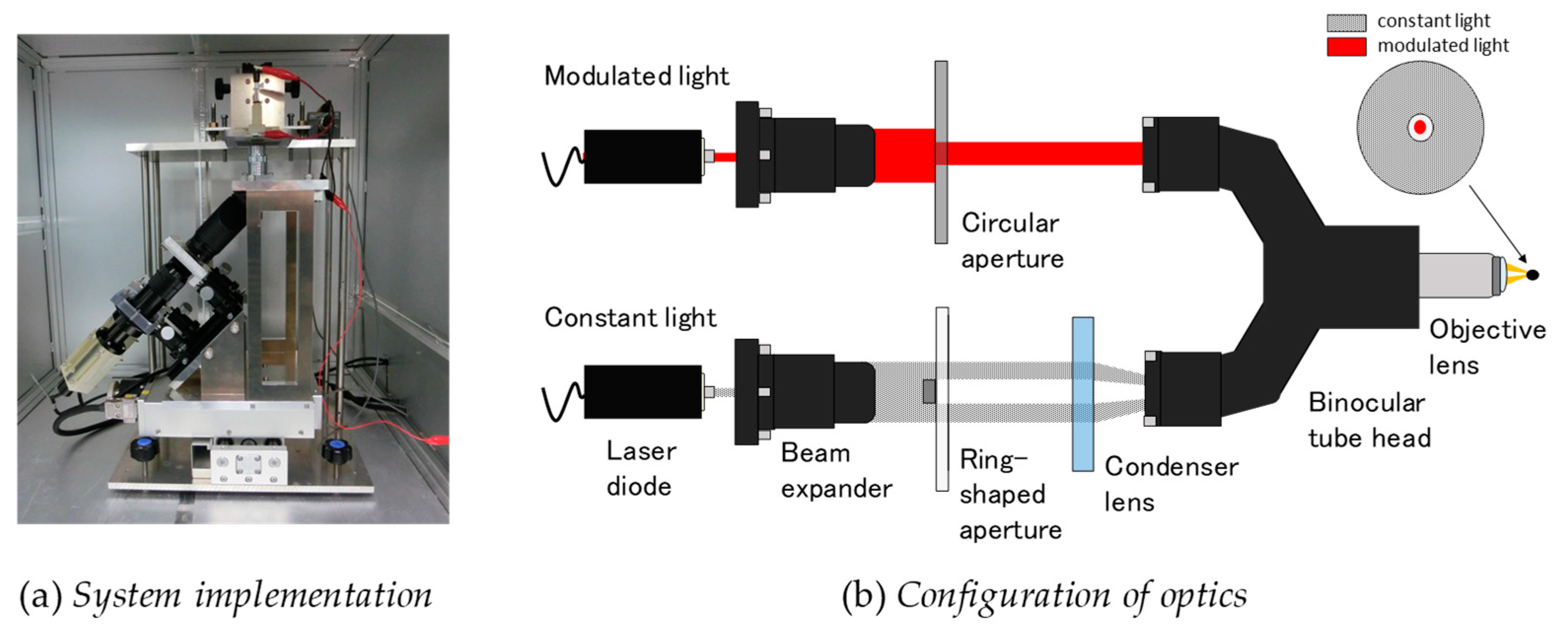
2. Materials and Methods
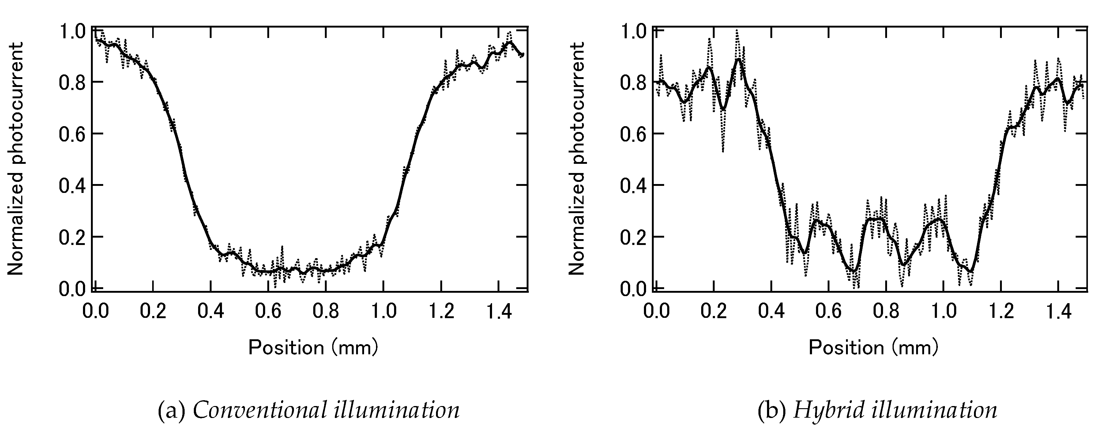
Sensor substrates were intrinsically the same as those used in our previous reports [9,10]. The surface of an n-type silicon wafer (1–10 ohm·cm, t = 200 μm) was insulated by a thermal oxide (SiO2) layer, then a layer of 50 nm silicon nitride (Si3N4) was deposited by LP-CVD as a sensing layer. Backside of the wafer was mechanically polished, then stripe-shaped gold electrodes were deposited as ohmic contacts.
Figure 2a shows the illumination system newly designed in this study. The optical system is schematically depicted in Figure 2b. Light beams from two laser diodes (λ = 832 nm, DPS-3001, NEOARK Corp., Japan), one modulated and one constant, go through ×10 beam expanders (LBE-10L, SIGMAKOKI Co. Ltd., Japan). They go through circular and ring-shaped apertures, respectively, and are mixed in a binocular tube (CH3-B145, Olympus Corp., Japan). The synthesized beam is focused onto the backside of sensor by an objective lens (ULWD MIRPlan50, Olympus Corp., Japan). Those optics were mounted on an X-Y stage (ALD-115-E1P, Chuo Precision Industrial Co. Ltd., Japan). The scanning of the sensor and the acquisition of the photocurrent were controlled by a homemade measurement software written in LabVIEW® (National Instruments Corp., USA).
To optimize the hybrid illumination, the gap between the modulated light and the ring-shaped constant light needs to be adjusted. In addition, the modulated light must be focused onto the backside of the sensor. The focal point of the constant light was displaced from that of the modulated light so that a ring-shaped illumination surrounded the focused modulated light as shown in Figure 3a. Figure 3b shows an example pattern of hybrid illumination. The beam of the modulated light was focused at the center, surrounded by the constant light with a certain gap between them.

3. Results

According to the experimental result, the photocurrent decreased as increasing of the intensity of the constant light was increased (data not shown), which suggested enhanced recombination due to photocarriers excited by the constant illumination.
The spatial resolution of the measurement was evaluated from photocurrent profiles across the edge of a photo-resist pattern deposited on the sensor surface. It was found that the spatial resolution depends on the intensity of the constant light and that of the modulated light. On the other hand, when the intensity of the constant light became excessive, the S/N ratio of the sensor signal was decreased. The optimized combination of the intensity of the modulated light and that of the constant light in this system was 0.002 mW and 0.7 mW, respectively.
In addition, it was also found that the spatial resolution could be enhanced as the inner diameter of the constant illumination was narrowed. Figure 4 shows the profile of the photocurrent corresponding to the photo-resist pattern (four striped pattern with a width and space of 100 μm). Under the conventional illumination, the striped pattern could not be recognized. On the other hand, after the optimization of the inner diameter of the ring and the intensities of the two beams, the stripe pattern could be clearly distinguished under the novel hybrid illumination. A spatial resolution of about 80 μm was achieved with the hybrid illumination, which was 40 μm better than that achieved with the conventional illumination. It was clearly demonstrated that the hybrid illumination proposed in this study could enhance the spatial resolution of the order of few tens of microns by effectively restraining the diffusion of photocarriers.

Acknowledgments

This work was supported by JSPS KAKENHI Grant Number 24310098. A part of this research was carried out at the Machine Shop Division of Fundamental Technology Center, Research Institute of Electrical Communication, Tohoku University.

Conflicts of Interest

The founding sponsors had no role in the design of the study; in the collection, analyses, or interpretation of data; in the writing of the manuscript, and in the decision to publish the results.

References

  1. Nakao, M.; Yoshinobu, T.; Iwasaki, H. Scanning-laser-beam semiconductor pH-imaging sensor. Sens. Actuators B 1994, 20, 119–123. [Google Scholar] [CrossRef]
  2. Hafeman, D.G.; Parce, J.W.; McConnell, H.M. Light-addressable potentiometric sensor for biochemical systems. Science 1988, 240, 1182–1185. [Google Scholar] [CrossRef] [PubMed]
  3. Nakao, M.; Yoshinobu, T.; Iwasaki, H. Improvement of spatial resolution of a laser-scanning pH-imaging sensor. Jpn. J. Appl. Phys. Part 2-Lett. 1994, 33, L394–L397. [Google Scholar] [CrossRef]
  4. Krause, S.; Moritz, W.; Talabani, H.; Xu, M.; Sabot, A.; Ensell, G. Scanning photo-induced impedance microscopy—Resolution studies and polymer characterization. Electrochim. Acta 2006, 51, 1423–1430. [Google Scholar] [CrossRef]
  5. Chen, L.; Zhou, Y.L.; Jiang, S.H.; Kunze, J.; Schmuki, P.; Krause, S. High resolution LAPS and SPIM. Electrochem. Commun. 2010, 12, 758–760. [Google Scholar] [CrossRef]
  6. Moritz, W.; Yoshinobu, T.; Finger, F.; Krause, S.; Martin-Fernandez, M.; Schöning, M.J. High resolution LAPS using amorphous silicon as the semiconductor material. Sens. Actuators B 2004, 103, 436–441. [Google Scholar] [CrossRef]
  7. Moritz, W.; Gerhardt, I.; Roden, D.; Xu, M.; Krause, S. Photocurrent measurements for laterally resolved interface characterization. Fresenius J. Anal. Chem. 2000, 367, 329–333. [Google Scholar] [CrossRef]
  8. Miyamoto, K.; Seki, K.; Guo, Y.; Wagner, T.; Schöning, M.J.; Yoshinobu, T. Enhancement of the spatial resolution of the chemical imaging sensor by a hybrid fiber-optic illumination. Procedia Eng. 2014, 87, 612–615. [Google Scholar] [CrossRef]
  9. Miyamoto, K.; Itabashi, A.; Wagner, T.; Schöning, M.J.; Yoshinobu, T. High-speed chemical imaging inside a microfluidic channel. Sens. Actuators B Chem. 2014, 194, 521–527. [Google Scholar] [CrossRef]
  10. Miyamoto, K.; Yu, B.; Isoda, H.; Wagner, T.; Schöning, M.J.; Yoshinobu, T. Visualization of the recovery process of defects in a cultured cell layer by chemical imaging sensor. Sens. Actuators B Chem. 2016, 236, 965–969. [Google Scholar] [CrossRef]
Figure 1. (a) Schematic view of chemical imaging sensor scanned by a modulated light beam. Carrier diffusion in cases of (b) conventional illumination and (c) hybrid illumination proposed in this study, respectively.
Proceedings 01 00477 g001
Figure 2. (a) Implementation of the measurement system in this study; and (b) schematic configuration of optics.
Proceedings 01 00477 g002
Figure 3. (a) Displacement between focal points of modulated light and constant light; and (b) an example of hybrid illumination.
Proceedings 01 00477 g003
Figure 4. Photocurrent profile across the striped photo-resist pattern with a width of 100 μm.
Proceedings 01 00477 g004
Publisher’s Note: MDPI stays neutral with regard to jurisdictional claims in published maps and institutional affiliations.

