Flow-Ratio Monitoring in a Microchannel by Liquid-Liquid Interface Interferometry †
by
 , and
, and
Martin Oellers
1,2,*, 
Frank Bunge
1,2,
Poornanchandra Vinayaka
1,2,
Sander van den Driesche
1,2 and
Michael J. Vellekoop
1,2 1
Institute for Microsensors, -actuators and -systems (IMSAS), University of Bremen, 28359 Bremen, Germany
2
Microsystems Center Bremen (MCB), Bremen, Germany
*
Author to whom correspondence should be addressed.
†
Presented at the Eurosensors 2017 Conference, Paris, France, 3–6 September 2017.
Proceedings 2017, 1(4), 498; https://doi.org/10.3390/proceedings1040498
Published: 30 August 2017
(This article belongs to the Proceedings of Proceedings of Eurosensors 2017, Paris, France, 3–6 September 2017)
Abstract
:A new method to monitor the relative flow rates of two different liquids in a microchannel is presented. By using a simple out-of-plane interferometer setup, shifts in the position of the interface between the two liquids can be determined. This label-free and real-time approach to observe the interface position yields the ratio of the flow rates. Applying an out-of-plane geometry allows the use of a flexible setup of chip-external optical components such as a laser and an image sensor, which is an advantage over fixed in-plane optics. With this measurement method we are able to monitor a change of about 1% of the relative flow rate between two fluidic inlets.
1. Introduction
The superiority of optofluidic devices over conventional solid-state devices is mainly based on their reconfigurability (such as refraction index control by replacement of a liquid in a microchannel). In such devices which employ microfluidics, non-mixing, coexisting fluid streams of multiple liquids within a single channel can be created. The resulting interface between those liquids in a laminar regime can be referred to as liquid-liquid (L2) interface. So far, many devices employ a planar configuration for generating such interfaces [1,2]. However, optical elements such as optical fibers and lenses have to be integrated into the microfluidic structures and therefore allow neither for realignment after the chip has been fabricated nor for adding additional optical components. The advantages of using external optical components [3] is an alternative to these existing concepts.
The presented device is built in an out-of-plane configuration where two liquids are horizontally positioned on top of each other next to a separate reference channel. The horizontal orientation of the chip facilitates optical measurements using an external laser. Therefore the L2- and reference-channel can be enlightened simultaneously by the same laser spot which is hard to realize in an in-plane configuration. It is essential in an interferometry setup to create a phase-shift of the incident light between sensing- and reference channel [4,5]. In our case this is provided by tuning the optical path length in the sensing channel by controlling the L2-interface position (e.g., increasing the thickness of one fluid while decreasing the thickness of the other). The position is changed by regulating the flow-ratios of the respective fluidic inlets.
Here we use low-cost equipment such as a pigtailed laser diode and a conventional CMOS camera-chip from a Raspberry Pi. In contrast to other in-plane fiber-optic interferometers and tuned cavity microfluidic devices we are not in need of a tunable light-source and spectrometer which is not only a simplification to the setup but also a cost-efficient way to determine the position of the L2-interface. By that we can monitor and adjust the ratio of the two liquids in the L2-channel which eradicates the need for flow sensors.
2. Materials and Methods
A photograph of the device is shown in Figure 1a. The device is comprised of a reference channel and a second channel (in the following referred to as L2-channel) in which a flow consisting of two liquids can be created on top of each other as horizontal layers. The reference channel has two fluidic connections (inlet and outlet) whereas the L2-channel has three (two inlets and one outlet). The two inlets are used to create a horizontal L2-interface (two layers on top of each other) which is a well-established technique in microfluidics. Both channels are 2 mm wide and separated by a 300 µm wide wall of silicon. The fluidic inlets have a radius of 500 µm (inlet 1), the rectangular inlet (inlet 2) covers the whole width of the L2-channel (2 mm) and has a length of 400 µm.
The glass-encapsulated silicon chip has been fabricated in a cleanroom using standard microfabrication techniques, see Figure 1b–d. To get an accurate measure of the final channel-height, we used a Keyence VK-9710 3D confocal laser scanning microscope. The measurement gives a value of 392 µm, which is consistent with the silicon wafer datasheet that provides a height of 380 ± 15 µm. The measurement of the L2-interface position is based on double-slit interference of light travelling through both fluidic channels. This principle was also employed in the sensing of refractive indices [5]. Since the liquid in the reference channel is fixed and also the refractive indices of both horizontal liquid layers are known it is possible to calculate the change in position of the L2-interface when the numbers of oscillations on the CMOS camera-output are counted. From the formula for a double-slit interference pattern on a screen [5] one can infer the change in position of the L2-interface by the refractive indices of the two horizontally aligned liquids which is:
where λ is the wavelength of the laser light and n1 and n2 are the refractive indices of the liquids entering inlet 1 and 2 of the L2-channel, respectively. The interference measurements are performed using a 660 nm fiber-pigtailed laser-diode with an output power of 5 mW. The device in Figure 1 is covered with a double-slit mask which yields the interference pattern on a CMOS-Chip in Figure 2a,b. The double-slit mask is printed on a foil and connected to the bottom of the device, see Figure 2. The slits have a width of 600 µm and are separated by 1 mm. The CMOS camera has a pixel-pitch of 1.4 µm and the analysis is done using the output of one single pixel (see red and green dot in Figure 2a,b). Using deionized (DI) water (n1 = 1.335) and a four-molar solution of CaCl2 (n2 = 1.422) where the heavier liquid is placed at the bottom of the chip (provided at inlet 2) and lighter one is placed at the top (via inlet 1). The flow-rates used during the experiment are on the order of 50 nL/s, which for aqueous solutions and the characteristic length of the device (380 µm) yields a flow in the laminar regime. We use two neMESYS low pressure, pulsation free syringe pumps for the injection of liquids by placing the chip in a 3D-printed connector-structure. The volume of the L2-interface channel is 19.5 µL.
The measurement principle of the setup is shown in Figure 2 where monochromatic, coherent incident light travels through the L2- and reference channel, respectively. The light coming from the reference channel (right) never experiences any phase-shift. In Figure 2a the maxima (minima) of the light are depicted as solid (dashed) lines. Waves coming from both channels interfere and a pattern as in Figure 2a,b can be observed. As the position of the L2-interface is shifted to a lower position as in Figure 2b the exiting light of the L2-channel is phase-shifted which leads to a shift in the observed interference pattern.
3. Results
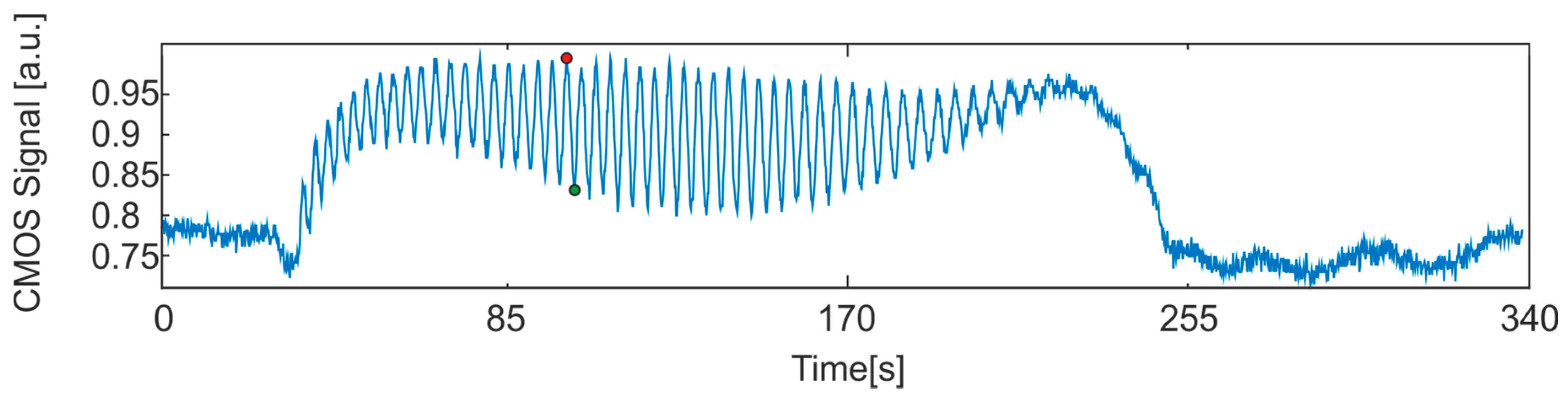
From Equation (1) the change in position (height) of the L2 interface can be calculated for each fringe which for the given values of n1, n2 and λ yields a value of 7.6 µm. In order to measure the height of the channel by interference, we first filled the L2-channel with a four-molar CaCl2-solution and started replacing this liquid with DI-water with a flow-rate of 50 nL/s. Hence, at t = 0 in Figure 3 the channel was completely filled with CaCl2-solution and it took around 40 s until the solution was starting to be replaced by DI water when the first oscillations were observed.
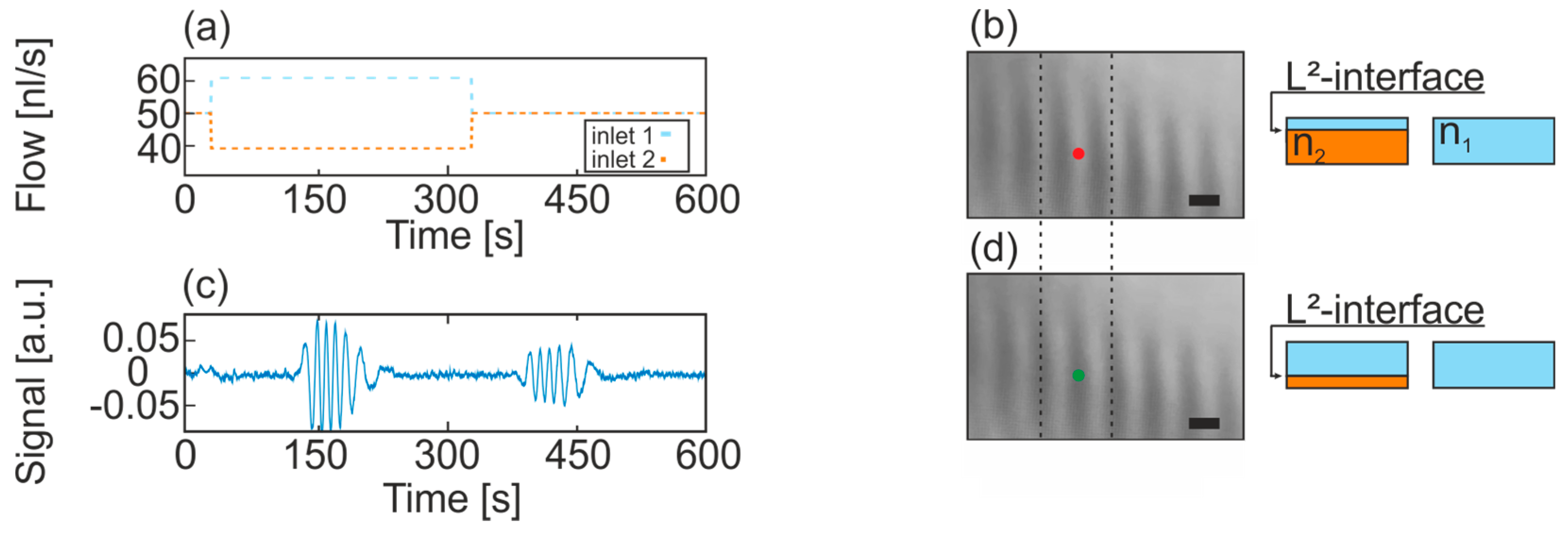
The number of fringes seen in Figure 3 is a measure of the distance the L2-interface has been displaced and a direct measure of the L2-channel height. If we multiply the 51 oscillations with ΔL the total distance the L2-interface has been shifted is 387 µm. This is in good agreement with the height extracted from the confocal laser spectroscopy measurements of 392 µm. To verify full control over the L2-interface we apply a flow-rate of 50 nL/s for both inlets 1 and 2 prior to starting the experiment shown in Figure 4. After waiting for 90 s, the flow-rates of the inlets are altered according to Figure 4a. Because of the equal flow rates the L2-interface will be positioned in the middle of the L2-channel. At t = 30 s the flow-rates are increased for inlet 1 and decreased for inlet 2 by 10 nL/s, respectively, which results in a repositioning of the L2-interface. The interference signal can be observed after 150 s in Figure 4c. As there are six fringes, the distance the L2-interface has been shifted can be calculated to 45 µm. Once a stationary position of the L2-interface is reached, no further shift in the interference-pattern is observed. As the flow-rates are tuned back to their initial values the L2-interface returns to its position in the middle of the channel which can be observed by the second interference-signal after 450 s. Within the 6 fringes, at least 4 positions per fringe can be determined, yielding a resolution of about 0.4 nL/s in flow change (about 1% of the flow rate).
4. Conclusions
We have presented an L2-interface interferometer fabricated from glass-encapsulated silicon. Choosing an out-of-plane geometry and creating a horizontal L2-interface allows for using chip-external optical components as well as a low-cost measurement setup. By using interference, we can monitor and adjust the position of an L2-interface in real-time without the use of any labeling and monitor a change in relative flow-rate of two different fluidic inlets of about 1%.
Acknowledgments
The authors would like to thank M. Kirsch, E. Ritter, C. Habben, I. Ersöz and I. Michels for the fabrication of the devices as well as F. Lucklum for 3D-printing of the fluidic connector structure. We thank all the above mentioned for fruitful discussions.
Conflicts of Interest
The authors declare no conflict of interest.
References
- Rosenauer, M.; Vellekoop, M.J. Characterization of an on-chip reconfigurable 3D optofluidic microlens by confocal laser scanning microscopy. Procedia Eng. 2010, 5, 440–443. [Google Scholar] [CrossRef]
- Wolfe, D.; Conroy, R.; Garstecki, P.; Mayers, B.; Fischbach, M.; Paul, K.; Prentiss, M.; Whitesides, G. Dynamic control of liquid-core/liquid-cladding optical waveguides. Proc. Natl. Acad. Sci. USA 2004, 101, 12434–12438. [Google Scholar] [CrossRef] [PubMed]
- Brandhoff, L.; Vellekoop, M.J. Optofluidic out-of-plane interferometer. In Proceedings of the IEEE Sensor, Baltimore, MD, USA, 3–6 November 2013. [Google Scholar]
- Lapsley, M.; Chiang, I.; Zheng, Y.; Ding, X.; Mao, X.; Huang, T. A single-layer, planar, optofluidic Mach-Zehnder interferometer for label-free detection. LOC 2011, 11, 1795–1800. [Google Scholar] [CrossRef] [PubMed]
- Sumriddetchkajorn, S.; Chaitavon, K.; Nukeaw, J. A free-space interferometric refractometer structure with simple microfluidic chips. IEEE Sens. J. 2012, 12, 404–409. [Google Scholar] [CrossRef]
Figure 1.
(a) Photograph of a glass-encapsulated silicon device with circular (inlet 1) and rectangular (inlet 2) fluidic connections. The scale bar at the upper left is 2 mm. (b–d) Fabrications steps including (b) powder blasting of glass, (c) anodic bonding of silicon to glass, DRIE of silicon, and (d) anodic bonding of a second glass-wafer. A cross-section of a plane-cut taken along the dotted red line of (a) is shown in (d). The sketch shows the inlets and outlet for the creation of two horizontally aligned (L2) liquid layers.
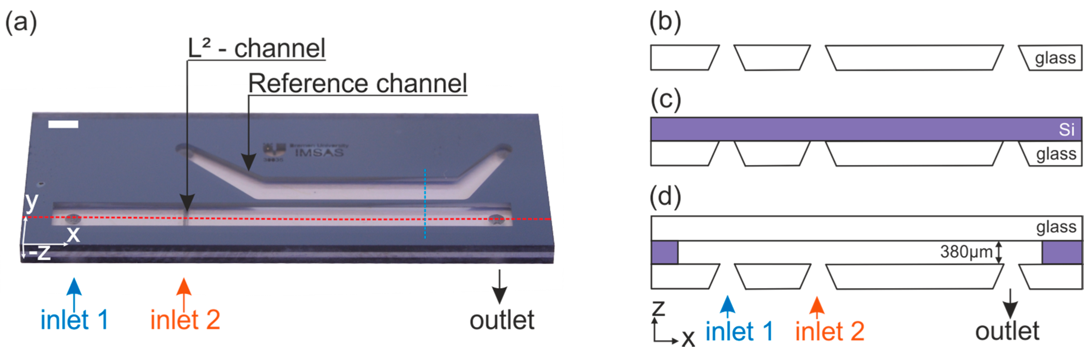
Figure 2.
Measurement principle showing a plane-cut of the device along the blue dotted line in Figure 1a in two different states of the L2-channel in (a,b). Solid (dashed) lines represent a wave-maximum (minimum).
Figure 2.
Measurement principle showing a plane-cut of the device along the blue dotted line in Figure 1a in two different states of the L2-channel in (a,b). Solid (dashed) lines represent a wave-maximum (minimum).
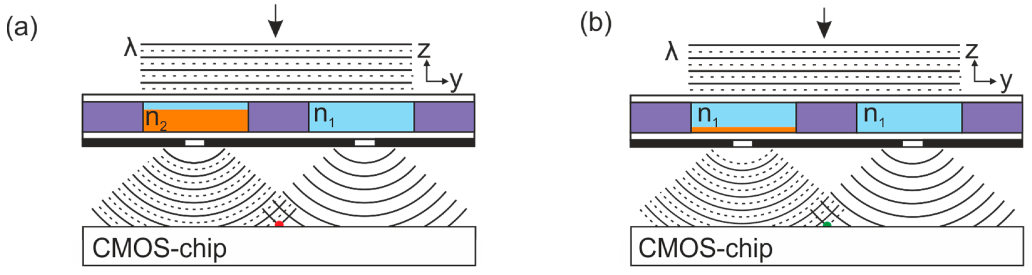
Figure 3.
Unprocessed CMOS-signal taken from a single pixel as indicated in Figure 2. The green and orange dots correspond to the interference maximum and -minimum shown in Figure 2, respectively.

Figure 4.
(a) Change in flow-rates of both inlets over time. (c) Background-subtracted signal of the CMOS-chip from one single pixel (compare with Figure 2). (b,d) Images taken from CMOS-camera at two different times (compare red and green dot in Figure 2) and L2-interface positions. The scale bar is 40 µm.

Publisher’s Note: MDPI stays neutral with regard to jurisdictional claims in published maps and institutional affiliations. |
© 2017 by the authors. Licensee MDPI, Basel, Switzerland. This article is an open access article distributed under the terms and conditions of the Creative Commons Attribution (CC BY) license (https://creativecommons.org/licenses/by/4.0/).
Share and Cite
MDPI and ACS Style
Oellers, M.; Bunge, F.; Vinayaka, P.; Driesche, S.v.d.; Vellekoop, M.J. Flow-Ratio Monitoring in a Microchannel by Liquid-Liquid Interface Interferometry. Proceedings 2017, 1, 498. https://doi.org/10.3390/proceedings1040498
AMA Style
Oellers M, Bunge F, Vinayaka P, Driesche Svd, Vellekoop MJ. Flow-Ratio Monitoring in a Microchannel by Liquid-Liquid Interface Interferometry. Proceedings. 2017; 1(4):498. https://doi.org/10.3390/proceedings1040498
Chicago/Turabian StyleOellers, Martin, Frank Bunge, Poornanchandra Vinayaka, Sander van den Driesche, and Michael J. Vellekoop. 2017. "Flow-Ratio Monitoring in a Microchannel by Liquid-Liquid Interface Interferometry" Proceedings 1, no. 4: 498. https://doi.org/10.3390/proceedings1040498