Proceeding Paper

Vertical 3D GaN Nanoarchitectures towards an Integrated Optoelectronic Biosensing Platform in Microbial Fuel Cells †

1
Institute of Semiconductor Technology (IHT), TU Braunschweig, 2, 38106 Braunschweig, Germany
2
Laboratory for Emerging Nanometrology (LENA), TU Braunschweig, 2, 38106 Braunschweig, Germany
3
Institute of Environmental and Sustainable Chemistry (IÖNC), TU Braunschweig, 2, 38106 Braunschweig, Germany
4
MIND-IN2UB, Department of Engineering-Electronics, University of Barcelona, 585, 08007 Barcelona, Spain
*
Author to whom correspondence should be addressed.
Presented at the Eurosensors 2017, Paris, France, 3–6 September 2017.
Proceedings 2017, 1(4), 508; https://doi.org/10.3390/proceedings1040508
Published: 4 August 2017
(This article belongs to the Proceedings of Proceedings of Eurosensors 2017, Paris, France, 3–6 September 2017)

Abstract

:
An integrated nano-optoelectronic biological sensor system is developed to obtain insights of the biochemical and physical processes of Geobacter sulfurreducens-based biofilm growth inside a miniaturized microbial fuel cell (MFC) reactor. Gallium nitride (GaN), which was used as a novel electrode material, has been investigated in terms of its biocompatibility and performance to transport the electrons delivered by the microorganisms. Moreover, in order to enhance the produced current density, vertical 3D GaN nanoarchitectures (i.e., arrays of nanowires and nanofins) with larger surface-to-volume ratios were fabricated using a top-down nanomachining method involving nanolithography and hybrid etching technique.

1. Introduction

Microbial fuel cells (MFCs) are an emerging sector of regenerative energies. Owing to the ability of generating electricity directly from chemical energy saved in organic compounds, they are well suited for being used as power saving modules in wastewater cleaning. The core component of a microbial fuel or electrolysis cell (MEC) is an electrochemically active biofilm (EAB), which is formed, e.g., by bacteria of the species Geobacter sulfurreducens. Although MFCs are being researched for several years, the electron transfer process, which is critical for the current production is not yet sufficiently understood for significantly increasing their power efficiency [1]. For targeted enhancement of MFCs, a comprehensive understanding of the bacterial metabolism is necessary. Therefore, a miniaturized portable MFC integrated with a nano-optoelectronic sensor platform is currently developed to conduct in situ optical measurements, which are intended to give insights into the biochemical and physical processes during the biofilm growth, including the relationships between the thickness of the grown biofilm and the bioelectrocatalytic current density [2].

2. Materials and Methods

2.1. Electrochemical Cell Setup

All bioelectrochemical measurements of the three-electrode system were performed using a potentiostat type VMP3 (BioLogic, France) connected to a homebuilt Teflon biofilm reactor with a reactor chamber volume of approximately 88 cm3 (Figure 1a,b). The surface area of the electrode directly in contact to the growth medium was kept at ~12.6 cm2. Here we used a transparent two-inch working electrode consisting of n-GaN (planar or nanowires) on a sapphire substrate. The MEC (Figure 1a,b) used in this work, consists of a working electrode on which a biofilm of bacteria predominantly of the species Geobacter sufurreducens grows. These bacteria oxidize acetate into CO2, protons and electrons and transfer the electrons to the working electrode, from which they pass through a wire to the counter electrode where they are required for the reduction of protons to hydrogen gas.

2.2. Sensor for Transmission Measurements

The integrated sensor system will monitor the continuous growth of EABs over a longer time, to obtain information about the biochemical processes occurring in the biofilm. Various already existing non-destructive optical measuring methods are evaluated, adapted for application on optical in situ characterization of biofilms and combined in a sensor platform. The first measurement method integrated into the system is the transmission measurement for the determination of the biofilm thickness with the purpose of differentiating increasing current density for reasons of the growth of the biofilm or increasing metabolic activity, respectively. Depending on the material of the working electrode, the thickness reaches a maximum value [2,3], which cannot be increased, despite enough growth medium being available. The reason for this is not yet fully understood. It is only known that the factors, e.g., high conductivity and roughness, have a positive effect on the biofilm thickness [1]. Therefore, with increasing film thickness, deeper lying bacteria are becoming poorly supplied with nutrients. Currently, the biofilm thickness can only be determined by means of very complex and expensive measuring methods, e.g., confocal laser scanning microscopy (CLSM) [1,2,3] or atomic force microscopy (AFM) [4].
Figure 1c shows the status of the first generation of a compact micro controlled sensor platform comprising two LEDs and two photodiodes as light sources or transmitted light detectors, respectively. Initially the extinction coefficient is approximated due to the biofilm density change caused by gas inclusions and dead bacteria as shown by preliminary investigations with ITO and ITO/gold electrodes [2]. By cross-sectional imaging using CLSM, the thickness of the biofilm can be determined ex situ and used together with the intensity measured by the photodiode for calculating the extinction coefficient, so that it is known for later in situ measurements. If transparent electrode materials are used, the biofilm thickness can then be determined from the amount of light transmitted through the biofilm. Alternatively, the possibility of cultivating the bacteria directly on the LED material (GaN) should be investigated to achieve maximum light intensities and optimal coupling with the EAB to reduce environmental interferences. This requires biocompatibility of GaN, which was investigated within this work. Consequently, GaN simultaneously fulfills the function of the electron-emitting working electrode. As an extension, the use of 3D nanoLED [5] arrays will allow the determination of thicknesses with high spatial resolution, as well as holographic photographs.

2.3. GaN as Electrode Material

Two different electrode morphologies (i.e., A and B) were fabricated using metal-organic vapor phase epitaxy (MOVPE) on a commercial two-inch sapphire wafer of 430 μm thickness. The GaN layer sequence consists of an n-GaN nucleation layer of approximately 30 nm and:
  • For A: an n-GaN layer (2.3 µm, donor concentration ND = 1018 cm−3) and a 1.9 µm n-doped layer in the range of 1018–1019 cm−3. This working electrode was cleaned with isopropanol before usage.
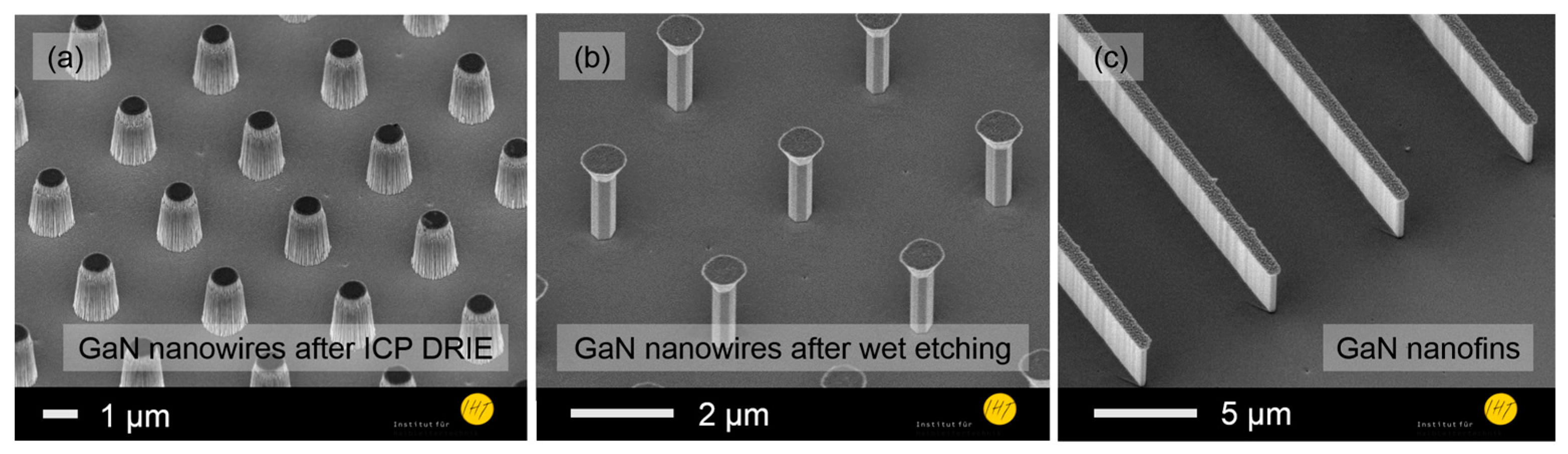
  • For B: an n-GaN layer (2.5 µm, ND = 1018 cm−3), a low doped GaN layer (1.5 µm, ND = 1016 cm−3) and an n-GaN layer (1.0 µm, ND = 1018 cm−3). Nanowires and nanofins (Figure 2) were fabricated by inductively coupled plasma deep reactive ion etching (ICP-DRIE), followed by wet etching for sidewall smoothing and wire diameter reduction [6]. The nanowire array had a pitch of ~2 µm, a height of about 1.45 µm and a diameter of 380 nm.

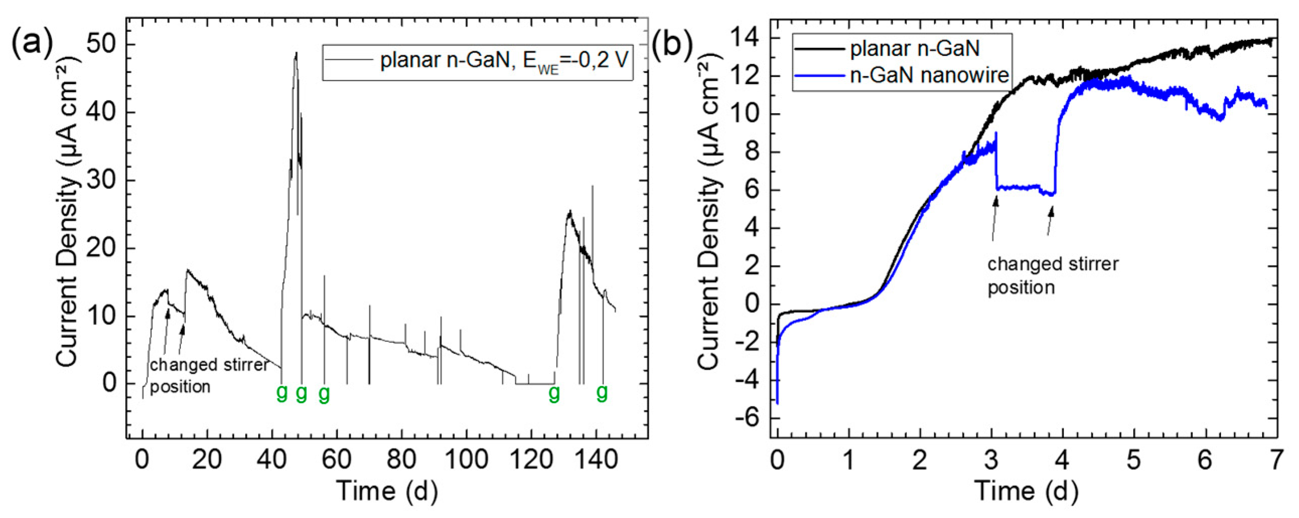
3. Experimental Results and Discussion

The EAB growth was performed under anaerobic conditions at 35 °C employing the same growth medium and inoculum source as Schmidt et al. [2]. The electrochemical characterization of GaN was carried out using chronoamperometry recorded at applied potential −0.2 V vs. Ag/AgCl reference electrode (Figure 3). In the case of 2D planar GaN material, current densities up to 48 μA cm−2 were measured proving the material compatibility in long-time biofilm growth processes. The reason for not reaching the maximum current again after the second medium exchange could be unwanted oxygen input into the biofilm reactor or possible biofilm detachment during growth medium exchange. With the use of the finished sensor system, a better understanding of the influences on the biofilm growth will be made possible and the measurements will then be repeated.
Furthermore, an MEC current density enhancement, at least at the beginning of the growth, was expected by utilizing vertical 3D GaN nanostructures with varied sizes and geometries (i.e., arrays of nanowires and nanofins) using GaN nanomachining techniques, which may enable the bacteria to grow either in the spaces between the GaN nanostructure sidewalls or directly on their top parts (Figure 2). This also increases the surface and can protect the initially growing isles of bacteria against the forces of the growth medium flow. The comparison between the initial biofilm growth of planar and nanostructured n-GaN shows a similar trend whereby the electrode with nanowires is providing somewhat lower current densities, thus not confirming the assumption so far. The current densities observed were not comparable with those of, for example, graphite or copper electrodes [3]. Further experiments with nanofins are intended to be added to the experiments with planar GaN and nanowires.

4. Conclusions

In this paper, it was shown that GaN is biocompatible and suitable as electrode material for use in MECs, regardless of producing lower current density than normally used electrodes (e.g., graphite and copper). We also presented the first steps towards an integrated sensor system coupled directly to the biofilm. More experiments using 3D GaN nanostructures are required to be performed to clarify and explain the effect of surface area enhancement.

Author Contributions

H.B., G.S. and H.S.W. developed the sensor system; I.M.C., M.F.F., K.S., F.Y. and S.M. provided planar or nanostructured GaN samples; H.B. and H.W. performed the experiments and analyzed the data; H.B. wrote the paper; J.D.P., H.S.W., A.W. and U.S. revised the paper and provided significant inputs on LED-based sensing or EAB characterization; H.S.W. and A.W. led the development of the optical system.

Acknowledgments

The authors thank J. Breitfelder for processing assistance and K.-H. Lachmund for technical support. This work is performed within projects of LENA-OptoSense and QUANOMET funded by the Lower Saxony Ministry for Science and Culture. H.B. thanks for the Georg-Christoph-Lichtenberg Ph.D. scholarship (Tailored Light). G.S. and H.S.W. acknowledge the support from Photonik Inkubator GmbH.

Conflicts of Interest

The authors declare no conflict of interest.

References

  1. Beyenal, H.; Babauta, J.T. Biofilms in Bioelectrochemical Systems: From Laboratory Practice to Data Interpretation, 1st ed.; Wiley: Hoboken, NJ, USA, 2015. [Google Scholar]
  2. Schmidt, I.; Gad, A.; Scholz, G.; Boht, H.; Martens, M.; Schilling, M.; Wasisto, H.S.; Waag, A.; Schröder, U. Gold-modified indium tin oxide as a transparent window in optoelectronic diagnostics of electrochemically active biofilms. Biosens. Bioelectron. 2017, 94, 74–80. [Google Scholar] [CrossRef] [PubMed]
  3. Baudler, A.; Schmidt, I.; Langner, M.; Greiner, A.; Schröder, U. Does it have to be carbon? Metal anodes in microbial fuel cells and related bioelectrochemical systems. Energy Environ. Sci. 2015, 8, 2048–2055. [Google Scholar] [CrossRef]
  4. Connolly, J.; Jain, A.; Pastorella, G.; Krishnamurthy, S.; Mosnier, J.-P.; Marsili, E. Zinc oxide and indium tin oxide thin films for the growth and characterization of Shewanella loihica PV-4 electroactive biofilms. Virulence 2011, 2, 489–490. [Google Scholar] [CrossRef] [PubMed]
  5. Waag, A.; Wang, X.; Fündling, S.; Ledig, J.; Erenburg, M.; Neumann, R.; Al Suleiman, M.; Merzsch, S.; Wei, J.; Li, S.; et al. The nanorod approach: GaN NanoLEDs for solid state lighting. Phys. Status Solidi 2011, 8, 2296–2301. [Google Scholar] [CrossRef]
  6. Yu, F.; Yao, S.; Römer, F.; Witzigmann, B.; Schimpke, T.; Strassburg, M.; Bakin, A.; Schumacher, H.W.; Peiner, E.; Wasisto, H.S.; et al. GaN nanowire arrays with nonpolar sidewalls for vertically integrated field-effect transistors. Nanotechnology 2017, 28, 95206. [Google Scholar] [CrossRef] [PubMed]
Figure 1. (a) 3D sketch of a homebuilt miniaturized bio-electrochemical reactor consisting of (1) the reactor cover frames, (2) the adhesive copper tape, (3) the counter electrode, (4) the O-rings, (5) the reactor chamber with (6) three tube fittings and (7) the GaN working electrode; (b) Scheme of a microbial electrolysis cell (MEC) with highlighted bacterial metabolism (inset); (c) Current status of the sensor system. The photodiode and LED board can be screwed on the outside of both rector sides.
Proceedings 01 00508 g001
Figure 2. Vertical 3D GaN nanoarchitectures in shapes of nanowires after (a) inductively coupled plasma deep reactive ion etching (ICP-DRIE) and (b) KOH-based wet chemical etching and (c) nanofins.
Proceedings 01 00508 g002
Figure 3. Figure 3. (a) Chronoamperogram of biofilms growing on 2D n-type GaN (g: medium exchange); (b) Comparison of the initial biofilm growth of planar and nanostructured n-GaN.
Proceedings 01 00508 g003
Publisher’s Note: MDPI stays neutral with regard to jurisdictional claims in published maps and institutional affiliations.

