Hermetic Cavities Using Gold Wafer Level Thermocompression Bonding †


1
LAAS-CNRS, Université de Toulouse, CNRS, 31077 Toulouse, France
2
Company Esterline, 18941 Bourges, France
*
Author to whom correspondence should be addressed.
†
Presented at the Eurosensors 2017 Conference, Paris, France, 3–6 September 2017.
Proceedings 2017, 1(4), 607; https://doi.org/10.3390/proceedings1040607
Published: 24 August 2017
(This article belongs to the Proceedings of Proceedings of Eurosensors 2017, Paris, France, 3–6 September 2017)
Abstract
:This paper presents the study of gold/gold thermocompression bonding at silicon wafer level. The first samples contains sealing rings and electrical pads, and are characterized on pull, and shear test showing bond strength similar to silicon/glass anodic bonding (10 MPa–80 MPa). A sealed cavity and a piezoresistor on a 30 µm-thick silicon membrane are added in the second samples. Helium test, membrane deflection and piezoresistor signal monitoring after aging 14 days at 250 °C confirm the vacuum stability inside the cavity after bonding.
1. Introduction
The use of wafer level packaging for MEMS fabrication offers many benefits as lower cost and higher reliability such as 3D integration, hermeticity and collective fabrication. Several bonding techniques exist to ensure hermeticity of micro-cavities as fusion, eutectic, fritted glass, anodic and thermo compression. However, when MEMS realization requires also electrical contact through the cavity, thermocompression bonding appears as a good candidate. The use of gold material for the electrical contacts and for the cavity sealing is widespread because of its advantages as very good electrical conductivity, low temperature process and very stable physical properties [1,2,3,4,5,6]. The present works is focused on the realization and qualification of micro-cavities with electrical contacts using Au/Au thermocompression wafer level bonding. After the description of process flow, test structures and technological bonding parameters, results are given on bonding quality and cavity hermeticity using bond strength measurements and membrane deflection using piezoresistor signal monitoring.
2. Experimental
2.1. Process Flow Description
The different layers obtained at the end of the process are described below. We use 4 inches 500 µm thick double-sided polished silicon wafers with 200 nm thick thermal SiO2. A 50 nm thick TiW diffusion barrier followed by 50 nm/500 nm thick Ti/Au seed layer is then evaporated before 3 µm thick gold electroplating inside photo patterned resin mold in order to define sealing rings and electrical pads. The electroplated gold has low tensile stress (20 MPa) and low roughness (20 nm). The photoresist mold as well as the seed layers and the diffusion barrier are then chemically etched.
2.2. Equipment and Bonding Parameters
The wafers alignment as well as the bonding process are done respectively in BA8 and SB6 SUSS Microtech equipment. During alignment, spacers located between the two bonded wafers allow obtaining vacuum inside the cavity (≈ 5.10–3 mbar). The parameters used for bonding were pre-established from the literature as well as by preliminaries experimental pull tests. Just before bonding, surface cleaning is performed using chemical piranha followed by ozone plasma treatment. The temperature and the contact pressure during bonding are set respectively to 420 °C and 5.7 MPa. A bonding time of 50 min is performed with theses parameters. A 1 mm graphite film is used between the upper silicon wafer and the piston of the sealing machine to homogenize the contact pressure.
2.3. Tests Structures
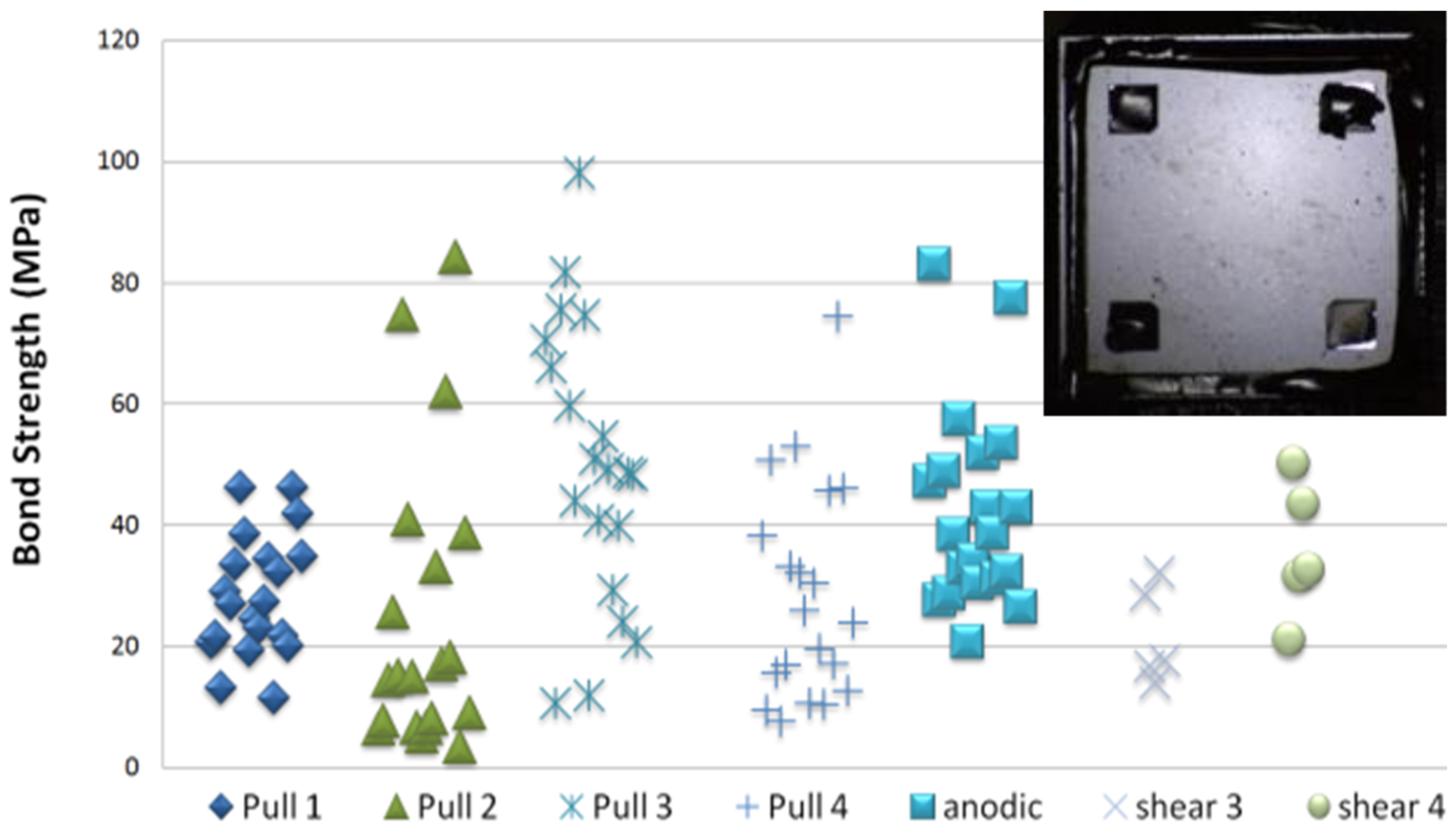
Two different tests structures were fabricated for bond strength (Figure 1) and hermeticity (Figure 2) experiments. Each chip has a dimension of 4700 µm × 4700 µm and 212 chips are distributed on the wafer. The first test structure will be used for pull and shear test in order to evaluate the mechanical strength of the Au/Au bonding. These values will be compared to reference values obtained by silicon/glass anodic bonding. In the second test structure, a piezoresistance is placed on a 30 µm thick and 2000 µm square silicon membrane in order to qualify the cavity hermeticity by measuring membrane deflection shift over time. Moreover fine leak tests with helium allowed us to characterize the loss of hermeticity after membrane breaking. For both test structures, the width rings was set to 300 µm. This value has been selected after mechanical simulations performed with COMSOL software. Also, in each structure, four 400 µm square metallic pads have been added all around the cavity in order to simulate the mechanical/electrical impact of electrical contacts in view of designing a future device.
3. Results
3.1. Gold Interface
In order to assess first the quality of Au/Au interface, we have done a cross section using diamond blade followed by polishing. FIB etching of the Au/Au interface has been also performed in order to remove parasitic burr (Figure 3). SEM observations show that we obtain a good sealing joint without voids or peeling.
3.2. Bond Strength
Four wafers were fabricated with the same bonding conditions described in § 2.1 to assess the reproducibility of the bonding. For each wafer, 20 dies collected from different wafer areas have been used for pull test (Figure 4). The dies were glued between two screws mounted then into the tools of the traction machine. Shear tests were also performed on dies from two wafers to compare the two techniques. Pull tests have been done also on 20 silicon/glass bonded dies. For pull tests, main results are higher than 10 MPa with an average of 33 MPa and a standard deviation of 18 MPa. We can notice a quite high dispersion on bond strength for dies coming from the same wafer. For comparison, average bond strength obtained with silicon/glass anodic bonding is 40 MPa with a standard deviation of 5 MPa. We can see that the dispersion obtained with the anodic bonding is also significant. Preliminary analysis have concluded that the strong inhomogeneity in bond strength are related to pull test experiment itself. This conclusion is corroborating with results obtained by shear tests that show less scattered values (average of 32 MPa and 6 MPa deviation).
In conclusion, we can say that numerous cells with Au/Au thermocompression bonding exhibit bond strength comparable or superior than those obtained with silicon/glass anodic bonding. Despite strong inhomogeneity in bond strength value, the fracture surface analysis shows generally cohesive failure in silicon even with low bond strength value. We can therefore conclude that Au/Au bonding is satisfactory. Bond strength analysis done with pull tests require then enough dies to reduce uncertainty and avoid bad interpretation.
3.3. Hermeticity
The vacuum created inside the cavity during bonding gives a 1 bar differential pressure on the silicon membrane. The membrane deflection is monitored with a mechanical profiler for the different cells on a wafer. It may be noted that 50% of the dies have membranes deflection close to 5 µm (depends on draft measure approximation) that is consistent with simulations. These deflections remained unchanged (shift lower than ±0.1 µm) after two months under room temperature and atmospheric pressure and after 24 h thermal cycling (−45 °C to 250 °C), validating the hermeticity of Au/Au bonding.
He tests under the standard specification were also done. To perform the wafer bonding leakage measurement, some dies with good vacuum have been used after breaking the deflected silicon membrane. The dies have been glued on a special tool connected to vacuum detector equipment (Figure 5). On one side of the sample vacuum has been pump down to 1.10−9 mbar, and on the other side, He has been injected. The mean leak measured by He detector was 10−8 mbar.L/s for the best dies structure bonded which correspond to an excellent hermeticity.
To monitored the membrane deviation more accurately and ensure the vacuum quality, one piezoresistor has been added on the membrane. The hermeticity reliability has been characterized by following the response of the piezoresistor after aging at 250 °C during 14 days for 6 cells (Table 1). The piezoreristance shift is lower than 250 ppm for the best cell that correspond to a 75 mbar variation inside the cavity.
4. Conclusions
Even if pull tests are often used for the qualification of bond strength, this technique don’t give reproducible results. Monitoring the bond strength value by this technique is then not a relevant parameter to assess accurately the bonding quality. However the hermeticity of micro-cavities fabricated with Au/Au thermocompression bonding has been validated thanks to direct silicon membrane deflection monitoring and also by following the value of a piezoresitor embedded on the membrane. The validation has been performed for a 2 months duration at room temperature and atmospheric pressure and for 24 h thermal cycling (−45 °C to 250 °C). In addition, the leak rate confirmed the good hermeticity inside the cavity of the bonded dies.
Acknowledgments
This work was partly supported by the french RENATECH network.
Conflicts of Interest
The authors declare no conflict of interest.
References
- Malik, N.; Tofteberg, H.R.; Poppe, E.; Finstad, T.G.; Schjølberg-Henriksenb, K. Environmental Stress Testing of Wafer-Level Au-Au Thermocompression Bonds Realized at Low Temperature: Strength and Hermeticity. ECS J. Solid State Sci. Technol. 2015, 4, P236–P241. [Google Scholar] [CrossRef]
- Tsau, C.H.; Spearing, S.M.; Schmidt, M.A. Low temperature wafer-level bonding for hermetic packaging of 3D microsystems. Micromech. Microeng. 2011, 21, 075006. [Google Scholar]
- Tsau, C.H.; Spearing, S.M.; Schmidt, M.A. Characterization of wafer-level thermocompression bonds. J. Microelectromech. Syst. 2004, 13, 6. [Google Scholar] [CrossRef]
- Taklo, M.M.V.; Storas, P.; Schjølberg-Henriksen, K.; Hasting, H.K.; Jakobsen, H. Strong, high-yield and low-temperature thermocompression silicon wafer-level bonding with gold. J. Micromech. Microeng. 2004, 14, 884. [Google Scholar] [CrossRef]
- Ishida, H. Low Temperature Hermetic Seal Bonding for Wafer Level MEMS Packaging Using Submicron Gold Particles with Stencil Printing Patterning, Braunschweig; ProceedingsWaferBond15. 2015.
- Kebabi, B.; Malek, C.K.; Ladan, F.R. Stress and microstructure relationships in gold thin films. Vacuum 1990, 41, 1353–1355. [Google Scholar] [CrossRef]
Figure 1.
Optical view of upper silicon die on the (left) and cross sectional drawing on the (right) for bond strength test structure.
Figure 1.
Optical view of upper silicon die on the (left) and cross sectional drawing on the (right) for bond strength test structure.

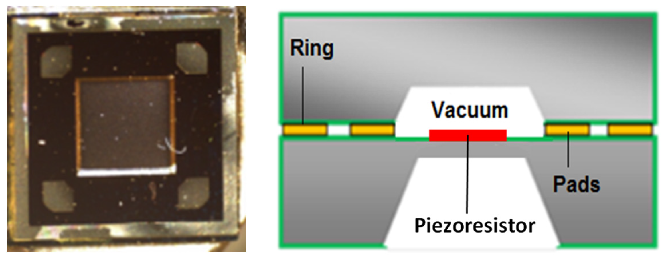
Figure 2.
Optical view of upper silicon die on the (left) and crosssectional drawing on the (right) for hermeticity test structure.
Figure 2.
Optical view of upper silicon die on the (left) and crosssectional drawing on the (right) for hermeticity test structure.

Figure 3.
Ring cross section view, Optical image after polishing (a); SEM image after FIB etching (b).
Figure 3.
Ring cross section view, Optical image after polishing (a); SEM image after FIB etching (b).

Figure 4.
Cohesive fracture on silicon die and bond strength obtained with pull and shear tests.

Figure 5.
He Hermiticity test on structure 2.


Table 1.
Piezoresistor shift after aging 14 days at 250 °C for 6 different cells.
| Cell Number | 1 | 2 | 3 | 4 | 5 | 6 |
|---|---|---|---|---|---|---|
| ΔR/R (ppm) | 248 | 568 | 333 | 3770 | 2370 | 1070 |
Publisher’s Note: MDPI stays neutral with regard to jurisdictional claims in published maps and institutional affiliations. |
© 2017 by the authors. Licensee MDPI, Basel, Switzerland. This article is an open access article distributed under the terms and conditions of the Creative Commons Attribution (CC BY) license (https://creativecommons.org/licenses/by/4.0/).
Share and Cite
MDPI and ACS Style
Charlot, S.; Pons, P.; Dilhan, M.; Vallet, I.; Brida, S. Hermetic Cavities Using Gold Wafer Level Thermocompression Bonding. Proceedings 2017, 1, 607. https://doi.org/10.3390/proceedings1040607
AMA Style
Charlot S, Pons P, Dilhan M, Vallet I, Brida S. Hermetic Cavities Using Gold Wafer Level Thermocompression Bonding. Proceedings. 2017; 1(4):607. https://doi.org/10.3390/proceedings1040607
Chicago/Turabian StyleCharlot, Samuel, Patrick Pons, Monique Dilhan, Isabelle Vallet, and Sebastiano Brida. 2017. "Hermetic Cavities Using Gold Wafer Level Thermocompression Bonding" Proceedings 1, no. 4: 607. https://doi.org/10.3390/proceedings1040607