Printed Sensors for Material Integrated Sensing: Functionalization of Semi-Finished Parts †

Institute for Microsensors, -actuators and -systems (IMSAS), Microsystems Center Bremen (MCB), University of Bremen, 28359 Bremen, Germany
*
Author to whom correspondence should be addressed.
†
Presented at the Eurosensors 2017 Conference, Paris, France, 3–6 September 2017.
Proceedings 2017, 1(4), 608; https://doi.org/10.3390/proceedings1040608
Published: 8 August 2017
(This article belongs to the Proceedings of Proceedings of Eurosensors 2017, Paris, France, 3–6 September 2017)
Abstract
:A new and innovative approach is presented to integrate sensors in materials and set up “smart materials”. Semi-finished parts are functionalized by printed sensors and printed interconnects. These functionalized parts are then further processed to components. This is a new and simple approach to integrate sensors in a material. Two examples of printed sensors and the process of integration are presented. One is a printed sensor on carbon weaves, integrated in carbon fiber reinforced plastic. The other one is a sensor structure printed on an aluminum sheet and integrated during high pressure die casting. Besides the benefits of this technological approach, challenges are focused in the paper as well.
1. Introduction
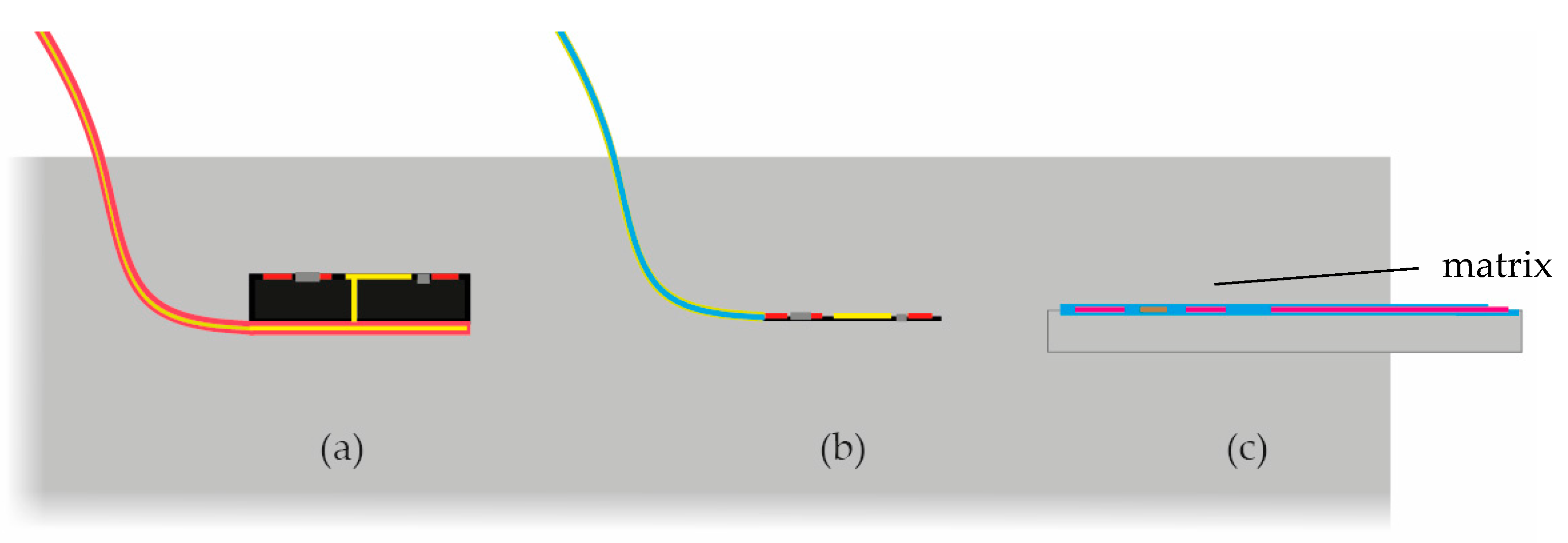
There is strong trend in getting physical measurement quantities, like strain or temperature, out of a material. This data is used to characterize production processes for example, or they are the basis for structural health monitoring systems. Most of the sensors are based on simple and well-known measurement principles like strain gauges, thermocouples, thermoresistive structures or piezoelectric ceramics. So far two different technology approaches have been used to integrate sensors in a material: PCB (Printed Circuit Board) technology and thin film technology. Both are exemplarily shown in Figure 1a,b where a sensor is brought into a matrix (material). In case of PCB technology, a sensor chip is mounted on a flexible or rigid board. To power the sensor and to send data out of the material, a cable or the flex board itself is leading out of the material. The characteristic size of such systems is a few hundred microns up to a few millimeters. One example is a sensor integrated in concrete [1,2], another example is piezoelectric transducer integrated in aluminum [3,4]. With this technology approach, sensors can be integrated in materials. The parts are relatively large and a relatively large amount of different materials are brought into the matrix. Regardless of whether the sensor material and the materials for the interconnections are either more flexible or more rigid than the matrix, it will affect the structural behavior of the matrix. This has been discussed by the authors in [5] and is called the foreign body effect. In addition to a mechanical foreign body effect, a mismatch in the coefficient of thermal expansion or a mismatch in the thermal conductivity can have a huge impact on the matrix, especially when relatively large sensor and interconnects are used.
To reduce this foreign body effect and integrate sensors in minimal invasive way, a second approach is the use of thin film technology. Sensor structures are fabricated on thin foils on wafer level. One example is an interdigital structure on 5 µm thick polyimide foil to monitor the curing of carbon fiber reinforced plastics [6]. The characteristic size of such systems is less than 10 µm. The goal is to make sensors as tiny as possible, to bring them down to size of natural material inhomogeneity such as fiber bundles or trapped air. Since those tiny minimal invasive foil sensors work very well, the problem of a simple and minimal invasive interconnection technology has not been focused yet.
Our paper focuses on a new approach: Printed sensors for material integrated sensing. Sensors and the electrical interconnects are printed on semi-finished parts. Those functionalized parts are further processed to get smart components as shown in Figure 1c. In this case, interconnection is relatively simply done by printing technology. However, other challenges occur which are discussed in the next section.
2. Printed Sensors for Material Integrated Sensing
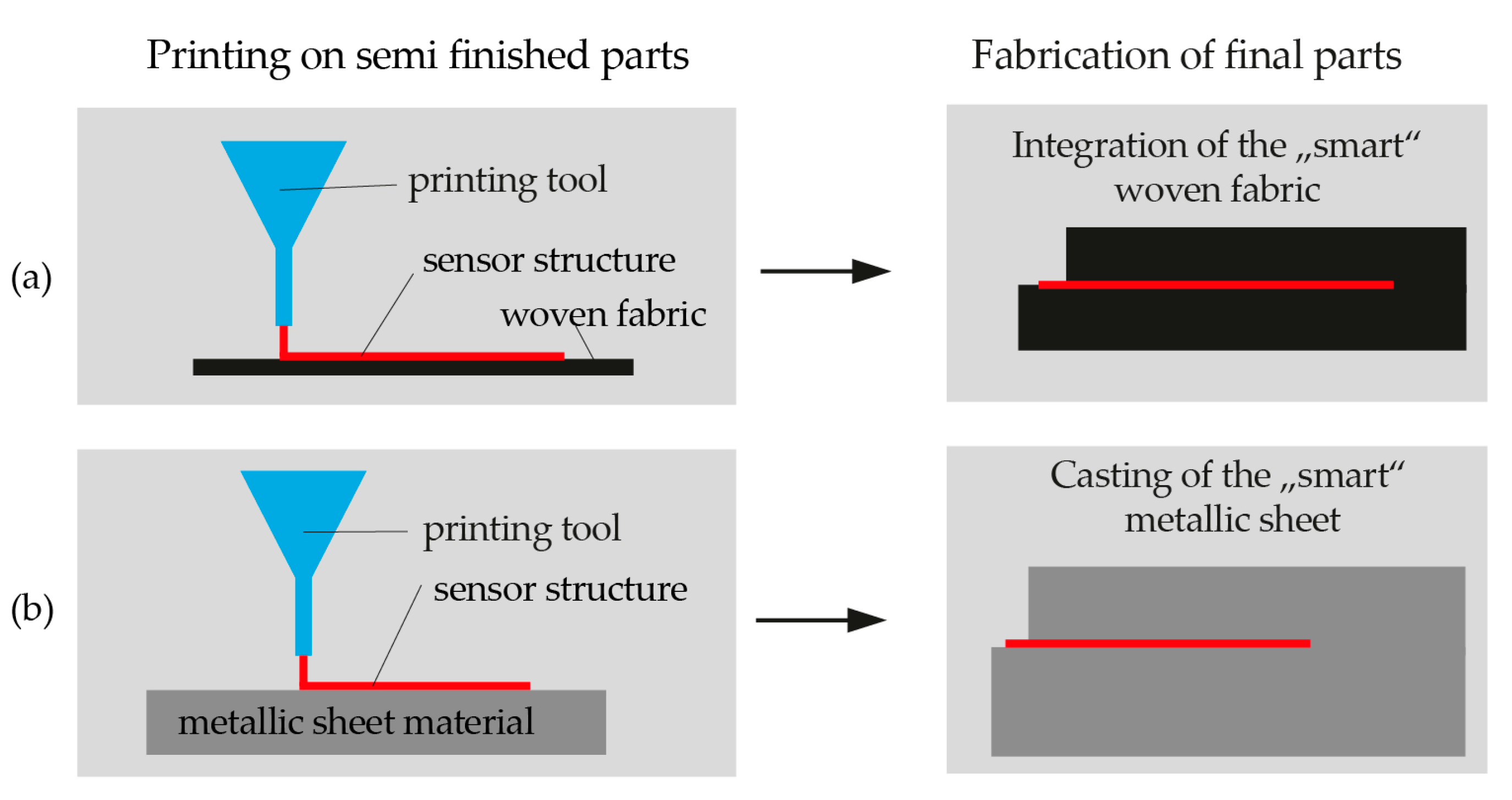
The idea to functionalize semi-finished parts by printing sensors on them, is shown in Figure 2. A sensor structure, made of conductive, semi conductive or insulating materials, is printed on a semi-finished part by e.g., screen printing, inkjet or roll to roll process. The semi-finished part could be a woven fabric as shown in Figure 2a, a metallic sheet (see Figure 2b) or any other material. After printing process, the semi-finished part is brought into the fabrication process of the final part. In comparison to thin film technology, the sensor structure and the interconnections are built up by printing process. No further cables or any other connection technology, which has to withstand the process of integration, are necessary. The semi-finished part is designed and integrated in a way that the electrical contacts lead to the outer edge of the final part. And since the process of building up the sensor is already adapted to the boundary conditions of the final integration process (e.g., thermal stress or thermal budget), the interconnections are optimized too.
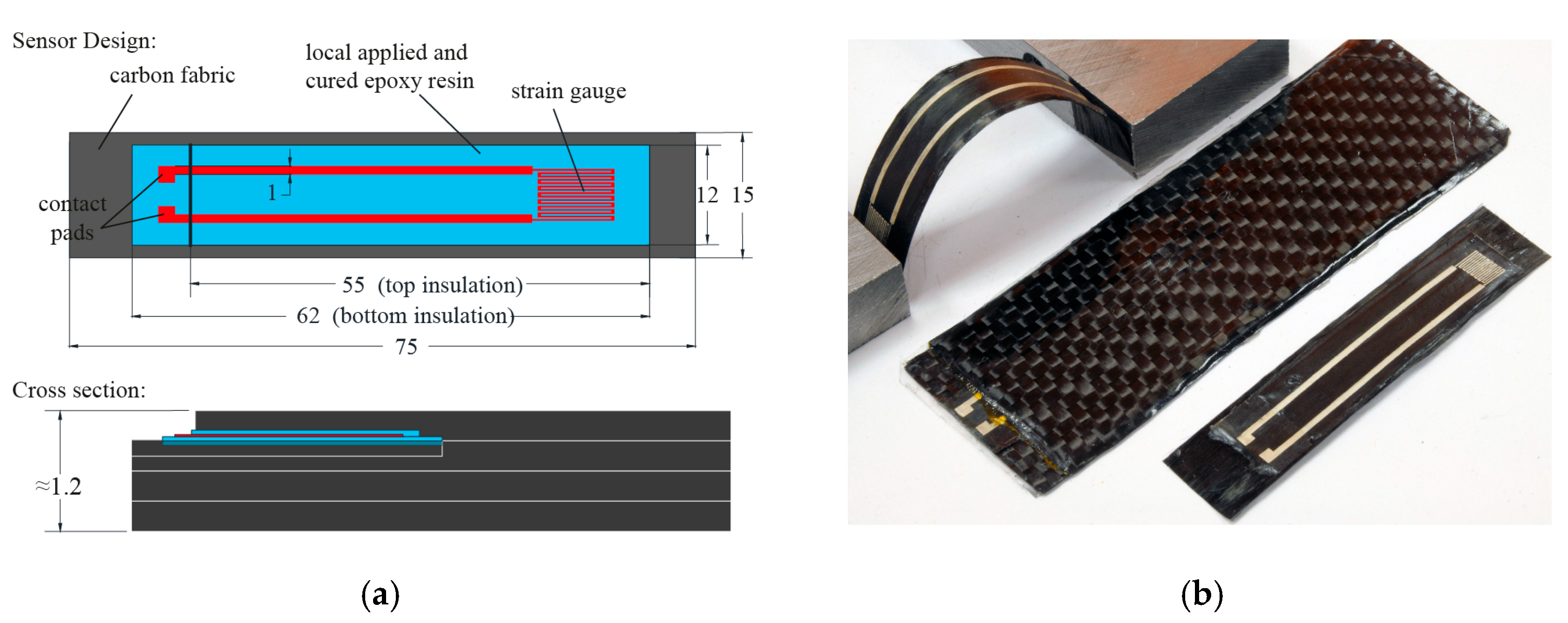
Two different approaches of printed and integrated sensors are shown in Figure 3 and Figure 4. The first example is a strain gauge printed on carbon weave and integrated in CFRP (carbon fiber reinforced plastics) [7] as seen in Figure 3. Therefore, the carbon weave is partially insulated and the sensor structures are printed on the carbon weave (similar to the process shown in Figure 2a). The “smart” woven fabric is then handled as a common woven fabric and integrated in a standard CFRP process. A second example is a resistive structure printed on an aluminum sheet [8], as shown in Figure 4. The sensor can be used as either a strain gauge or a thermoresistive temperature sensor. The “smart” aluminum sheet is integrated in a casting process. In both cases, aluminum and CFRP, the interconnections are printed. No further materials for packaging or cables are necessary. And in both cases the materials for the interconnections are already adapted to the process of integration.
If we compare printing technology with thin film technology, printing process is cheap, quickly adaptable, and up scaling to large structures is easy. No cleanroom technology is necessary and the sensors can be directly built up on the matrix material. In comparison to PCB technology, printing on semi-finished parts and integrating them is expected to be less invasive, because the characteristic length of such sensors is in the range of a few 10 µm.
However, the mechanical coupling between the semi-finished part, the sensor structures and the matrix is one of the most challenging things. If we get back to the examples shown in Figure 3, the coupling of the carbon weave is expected to be good. During fabrication of the final part, the fibers of the “smart” carbon weave merge with the resin of the matrix. In case of the “smart” aluminum sheet in Figure 4, the native oxide prevents a substance-to-substance bond, leading to a friction-locked connection. Getting a substance-to-substance bond between sheet and matrix is, so far, the most challenging thing from the view of the casting technology. Furthermore, there might be a risk of crack formation at the point, where interconnects lead out of the part. During long-term mechanical or thermal load, crack propagation might start from this point, leading to a failure of the part.
There is also a need of new materials like inks and pastes. So far, most inks are based on carbon or silver. Printable metals or metal alloys, especially polymer based pastes/inks for low temperature curing, are rarely found. Furthermore, new materials might be focused to print insulating materials for sensors integrated in casted iron.
3. Conclusions and Outlook
We have presented a new technology approach to integrate sensors in a material. Sensors are printed on semi-finished parts and then further processed to get “smart” components. With printing technology, the problem of interconnection technology is relatively simple, because they are printed in parallel with the sensor structures. Two examples, a smart woven fabric and a smart aluminum sheet, have been presented. We have shown that the approach of printing technology can be used to integrate sensors in a material. Advantages and challenges have been focused. One of the main challenges in the functionalization of semi-finished parts is the mechanical coupling at the interfaces of the semi-finished part and the matrix.
To reach the goal of a broad range of printed sensors for material integrated sensing, there is a need of design rules and material selection. Further investigations must focus on this. Tests on the mechanical coupling at the interfaces should be done. Besides this, new materials for printing conductive sensor structures and insulating materials must be developed.
Acknowledgments
The work is funded by the University of Bremen within the postdoctoral research project “AddSense: Additive manufacturing for local fabrication of sensor structures for material integrated sensing”. Furthermore, the authors thank Christoph Pille and Matthias Busse from Fraunhofer IFAM for integrating printed sensors in aluminum.
Author Contributions
The work presented in this paper was the collaboration of both authors. Walter Lang and Gerrit Dumstorff had the idea to integrate printed sensors in materials by functionalization of semi-finished parts. Gerrit Dumstorff did the writing of the manuscript. The advantages and challenges presented in this paper have been discussed by both authors.
Conflicts of Interest
The authors declare no conflict of interest. The founding sponsors had no role in the design of the study; in the collection, analyses, or interpretation of data; in the writing of the manuscript, and in the decision to publish the results.
References
- Qin, L.; Li, Z. Monitoring of cement hydration using embedded piezoelectric transducers. Smart Mater. Struct. 2008, 17, 055005. [Google Scholar] [CrossRef]
- Martínez, I.; Andrade, C. Examples of reinforcement corrosion monitoring by embedded sensors in concrete structures. Cem. Concrete Compos. 2009, 31, 545–554. [Google Scholar] [CrossRef]
- Pille, C. In-process-embedding of piezo sensors and RFID transponders into cast parts for autonomous manufacturing logistics. Smart Syst. Integr. 2010, Vol. 20, 1–10. [Google Scholar]
- Klassen, A.; Rübner, M.; Ilg, J.; Rupitsch, S.J.; Lerch, R.; Singer, R.F.; Körner, C. Influence of the fabrication process on the functionality of piezoceramic patch transducers embedded in aluminum die castings. Smart Mater. Struct. 2012, 21, 115014. [Google Scholar] [CrossRef]
- Dumstorff, G.; Lang, W. Investigations on the Impact of Material-Integrated Sensors with the Help of FEM-Based Modeling. Sensors 2015, 15, 2336–2353. [Google Scholar] [CrossRef] [PubMed]
- Boll, D.; Schubert, K.; Brauner, C.; Lang, W. Miniaturized flexible interdigital sensor for in situ dielectric cure monitoring of composite materials. IEEE Sens. J. 2014, 14, 2193–2197. [Google Scholar] [CrossRef]
- Dumstorff, G.; Lang, W. Strain gauge printed on carbon weave for sensing in carbon fiber reinforced plastics. In Proceedings of the IEEE Sensors, Orlando, FL, USA, 30 October–3 November 2016. [Google Scholar]
- Dumstorff, G.; Pille, C.; Tiedemann, R.; Busse, M.; Lang, W. Smart aluminum components: Printed sensors for integration into aluminum during high-pressure casting. J. Manuf. Process. 2017, 26, 166–172. [Google Scholar] [CrossRef]
Figure 1.
Three different technology approaches to integrate sensors in a matrix (material): (a) PCB technology; (b) thin-film technology; (c) printing technology.
Figure 1.
Three different technology approaches to integrate sensors in a matrix (material): (a) PCB technology; (b) thin-film technology; (c) printing technology.

Figure 2.
In the first step, sensor structures are printed on semi-finished parts like a woven fabric (a) or a metallic sheet (b) in example. These semi-finished “smart” parts are the integrated in the fabrication process.
Figure 2.
In the first step, sensor structures are printed on semi-finished parts like a woven fabric (a) or a metallic sheet (b) in example. These semi-finished “smart” parts are the integrated in the fabrication process.

Figure 3.
(a) Design of the printed sensor in the carbon weave and the cross section of the final CFRP-beam (dimensions are given in mm); (b) Carbon weave with printed strain gauge and the final CFRP- Beam. After processing the functionalized carbon weave is still flexible.
Figure 3.
(a) Design of the printed sensor in the carbon weave and the cross section of the final CFRP-beam (dimensions are given in mm); (b) Carbon weave with printed strain gauge and the final CFRP- Beam. After processing the functionalized carbon weave is still flexible.

Figure 4.
(a) Design of the functionalized semi-finished aluminum part and a cross section of the final part (dimensions are given in mm); (b) The final component with the integrated printed sensors, fabricated by high pressure die casting.
Figure 4.
(a) Design of the functionalized semi-finished aluminum part and a cross section of the final part (dimensions are given in mm); (b) The final component with the integrated printed sensors, fabricated by high pressure die casting.

Publisher’s Note: MDPI stays neutral with regard to jurisdictional claims in published maps and institutional affiliations. |
© 2017 by the authors. Licensee MDPI, Basel, Switzerland. This article is an open access article distributed under the terms and conditions of the Creative Commons Attribution (CC BY) license (https://creativecommons.org/licenses/by/4.0/).
Share and Cite
MDPI and ACS Style
Dumstorff, G.; Lang, W. Printed Sensors for Material Integrated Sensing: Functionalization of Semi-Finished Parts. Proceedings 2017, 1, 608. https://doi.org/10.3390/proceedings1040608
AMA Style
Dumstorff G, Lang W. Printed Sensors for Material Integrated Sensing: Functionalization of Semi-Finished Parts. Proceedings. 2017; 1(4):608. https://doi.org/10.3390/proceedings1040608
Chicago/Turabian StyleDumstorff, Gerrit, and Walter Lang. 2017. "Printed Sensors for Material Integrated Sensing: Functionalization of Semi-Finished Parts" Proceedings 1, no. 4: 608. https://doi.org/10.3390/proceedings1040608