Proceeding Paper

Monoclinic Zirconium Oxide Nanostructures Having Tunable Band Gap Synthesized under Extremely Non-Equilibrium Plasma Conditions †

Physics Department, Daulat Ram College, University of Delhi, Delhi 110007, India
*
Author to whom correspondence should be addressed.
Presented at the 1st International Online Conference on Nanomaterials, 1–15 September 2018; Available online: https://iocn-2018-1.sciforum.net/.
Proceedings 2019, 3(1), 10; https://doi.org/10.3390/IOCN_2018-1-05486
Published: 30 August 2018
(This article belongs to the Proceedings of IOCN 2018)

Abstract

:
Zirconium oxide (ZrO2) is a wide and direct band gap semiconductor used for the fabrication of optoelectronic devices. ZrO2 based optoelectronic devices span a wide optical range depending on the band gap of ZrO2 material. The band gap of ZrO2 can be tuned by fabricating it to the nanoscale. In this paper, we synthesized the ZrO2 nanostructures on quartz substrate using ZrO2 ions produced by the ablation of ZrO2 pellet due to high temperature, high density, and extremely non-equilibrium argon plasma in a modified dense plasma focus device. Uniformly distributed monoclinic ZrO2 nanostructures with an average dimension of ~14 nm were obtained through X-ray diffraction and scanning electron microscopy studies. The monoclinic phase of ZrO2 nanostructures is further confirmed from photoluminescence (PL) and Raman spectra. PL spectra show peaks in ultra-violet (UV), near-UV, and visible regions with tunable band gap of nanostructures. A similar tunability of band gap was observed from absorption spectra. The obtained structural, morphological, and optical properties are compared to investigate the potential applications of ZrO2 nanostructures in optoelectronic devices.

1. Introduction

Zirconium oxide (ZrO2) is an interesting semiconducting material with a wide band gap, which has been studied extensively to explore its fundamental properties for making highly efficient devices. The band gap of ZrO2 decreases with the increase of the processing temperature, which makes it more conductive, and hence it can be used in applications-oriented research. ZrO2 has a high melting point, high mechanical and thermal resistance, high dielectric constant, and low electrical conductivity. ZrO2 is also chemically stable with excellent hardness and biocompatibility, which renders it as a suitable candidate to be used for chemical, optical, dielectric, and mechanical applications [1,2,3]. ZrO2 has the potential to be used in making fuel cells [4], protective coatings for mirrors [3], and optoelectronic devices [5]. ZrO2 possess a high dielectric constant, which makes it an ideal candidate for the replacement of conventional gate oxide in field effect transistors in the future generation nanoelectronic devices.
The physical properties of ZrO2 are influenced significantly by its crystal structure. ZrO2 exists in three polymorphic phases depending upon the growth temperature, that is, monoclinic (exists at low temperatures below 1150 °C and is a thermodynamically stable phase), tetragonal (exists at intermediate temperatures within the range of 1150–2370 °C), and cubic (exists at very high temperatures greater than 2370 °C) [6]. The monoclinic crystal structure, being the thermodynamically stable phase, fulfills the stability requirement of ZrO2 based nanoelectronic devices. ZrO2, when fabricated at the nanoscale, results in emission peaks at short wavelengths, typically in the UV region, which have applications in making reading heads of compact discs (CDs) and increasing storage density of CDs [7,8]. In addition, the band gap of ZrO2 can be tuned at the nanoscale, which increases the applications, as well as the efficiency, of fabricated devices.
ZrO2 nanostructures have been fabricated in a variety of morphologies, such as nanoparticles [9], nanobars [10], nanobelts [11], nanowires [12], and nanotubes [13]. The fabrication of these different morphologies of ZrO2 nanostructures is mainly through chemical methods. However, chemical methods use several precursors and other reacting agents, which ultimately induces the impurity in nanostructures, making them unqualified for fabricating highly efficient devices. Plasma-assisted methods overcome the disadvantages of chemical methods in the fabrication of nanostructures. Moreover, the fabrication of ZrO2 nanostructures using plasma-assisted methods has not yet been reported in the literature. Thus, it is necessary to study the properties of ZrO2 nanostructures when fabricated using a plasma-assisted technique.
This paper reports the synthesis of ZrO2 nanostructures on quartz substrate using the material ions produced as a result of the ablation of ZrO2 pellet by the hot, dense, and extremely non-equilibrium argon plasma generated in a modified dense plasma focus (DPF) device. The properties of ZrO2 nanostructures, such as morphological, structural, and optical, have been studied and discussed in comparison with the earlier reports.

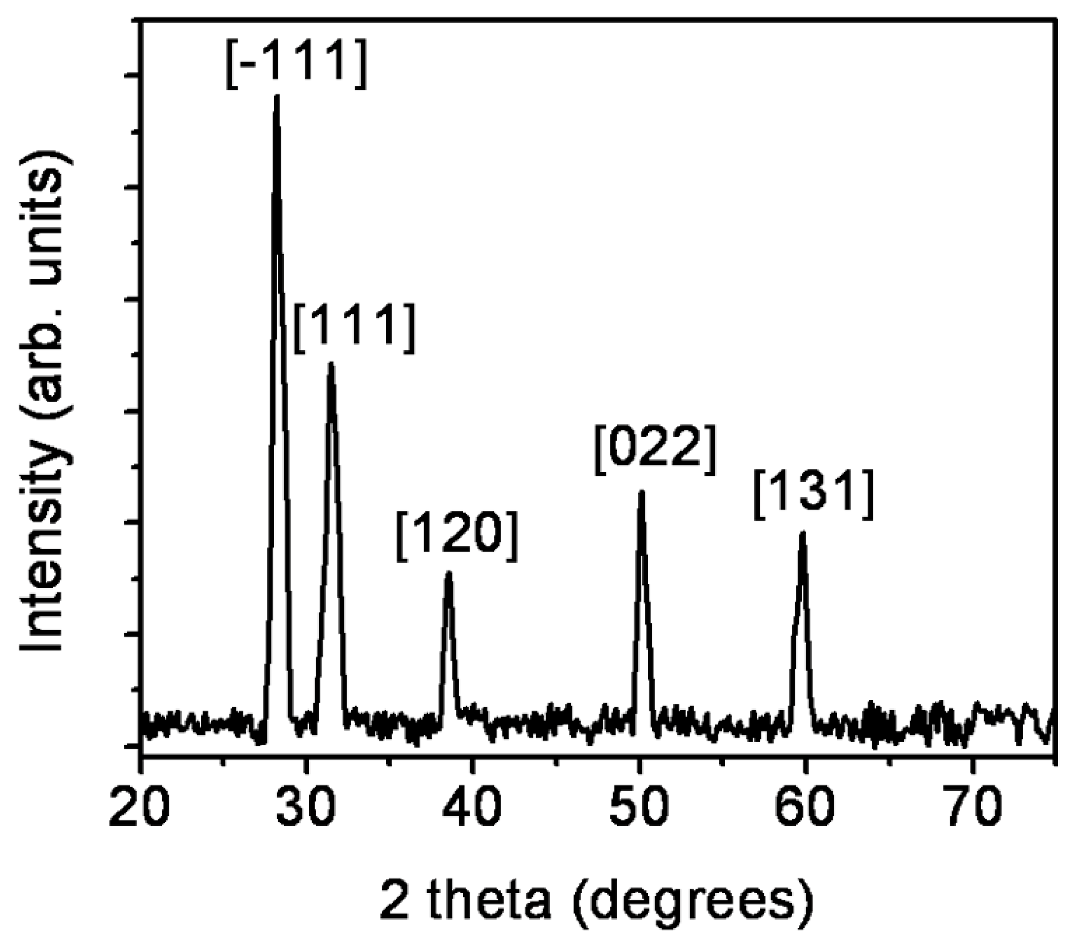
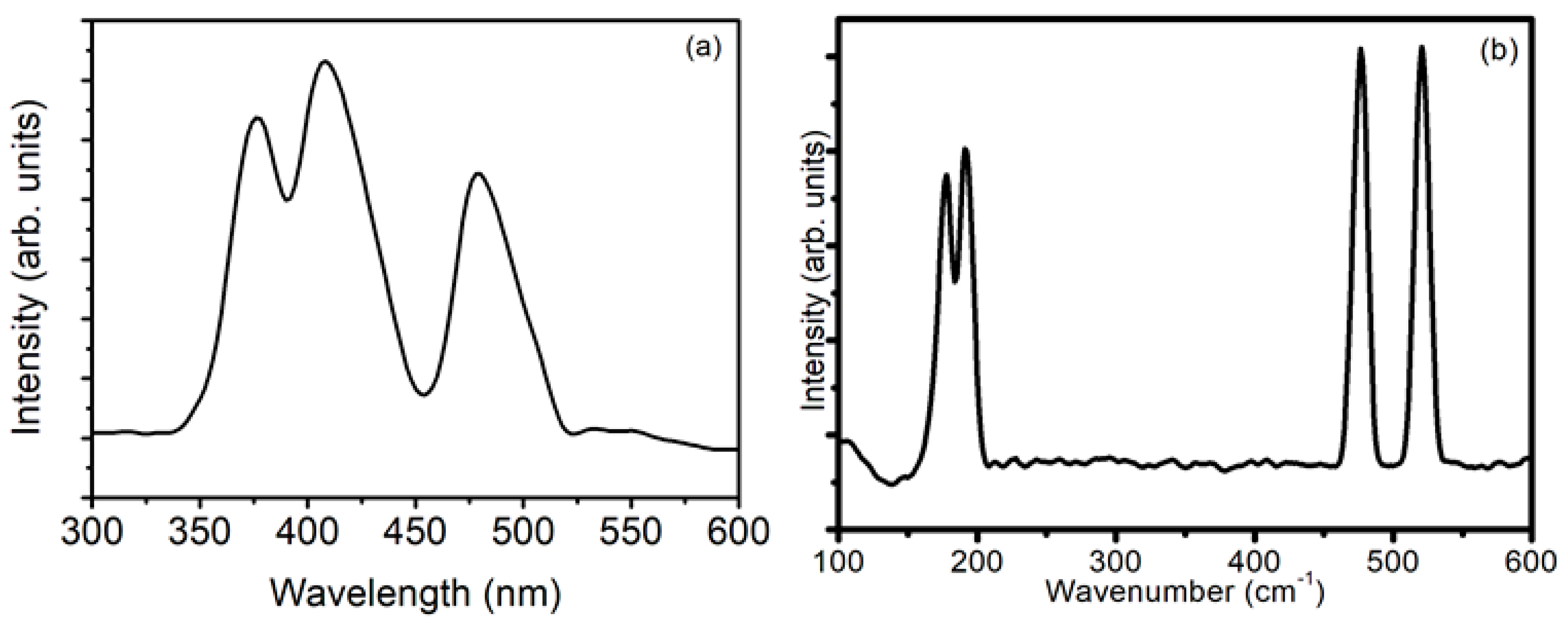
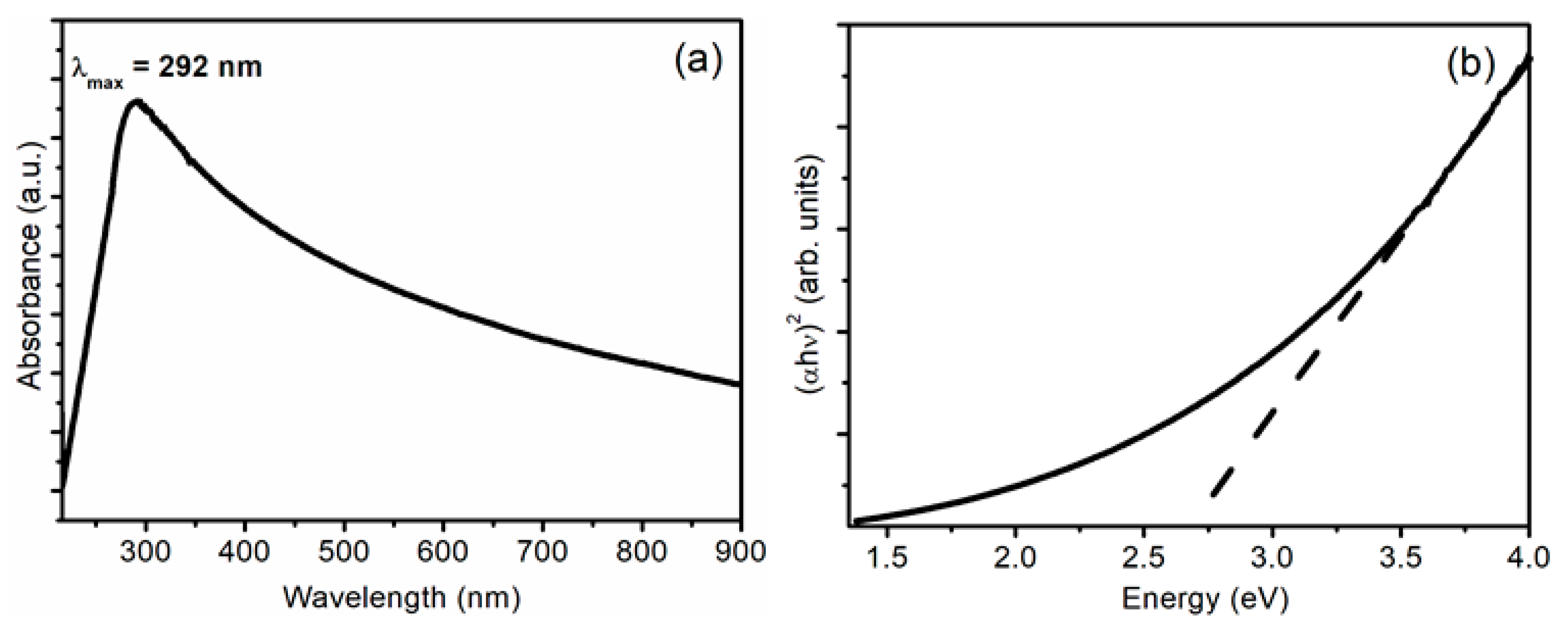
2. Results and Discussion

Figure 1a shows the scanning electron microscopy (SEM) image of the deposited sample, indicating formation of uniformly distributed ZrO2 nanostructures with a surface density of ~4100 nanostructures/μm2. The size distribution of ZrO2 nanostructures is shown in the inset of Figure 1a, and the peak of Gaussian profile in the histogram gives an average dimension of nanostructures of ~14 nm. The transmission electron microscopy (TEM) image shown in Figure 1b confirms the formation of nanostructures with morphology similar to that obtained in SEM results. However, it is difficult to estimate the size distribution from the TEM image, thus a typical nanostructure with a dimension of ~15 nm is shown by the arrow in Figure 1b. The morphology and dimensions of nanostructures obtained from the TEM results are in good agreement with those obtained from SEM results.
In order to investigate the crystalline phase of ZrO2 nanostructures, X-ray diffraction (XRD) studies were carried out. The XRD pattern shown in Figure 2 has crystalline diffraction peaks at 2θ values of 28.2°, 31.5°, 38.5°, 50.1°, and 59.8° corresponding to [−111], [111], [120], [022], and [131] planes, respectively, of monoclinic ZrO2 (ICDD File No. 37-1484). The grain dimension is found from Debye Scherrer’s equation.
D = 0.9 λ β cos θ ,
where D is grain dimension in nm, λ is wavelength in nm, β is full width at half maxima (FWHM) in radians, and θ is angle of diffraction corresponding to peak. The grain dimension was found individually for each peak of XRD pattern and the average was taken. The average grain dimension was found to be about 14 nm, which is in good agreement with the dimension of nanostructures obtained from the SEM and TEM results. The length of dislocation per unit volume, that is, dislocation density (δ), depends upon grain dimension (D), as follows:
δ = 1 D 2 ,
In addition, the strain (ε) produced in the film or nanostructures due to presence of such dislocations can be calculated using the following relation:
ε = β cos θ 4 ,
The obtained values of 2θ, θ, β, D, δ, and ε are summarized in Table 1. The average strain produced in nanostructures is ~2.5 × 10⁻³, indicating good quality of the deposited nanostructures.
The monoclinic structure of ZrO2 nanostructures was confirmed using photoluminescence (PL) and Raman spectra. The PL spectrum shown in Figure 3a has peaks at 376 nm (3.29 eV), 408 nm (3.04 eV), and 478 nm (2.59 eV). The peak obtained at 376 nm lies in the UV region, and arises as a result of the presence of oxygen vacancies in the nanostructures. These oxygen vacancies cause the extrinsic states between the valence band and conduction band to yield radiative transition at lower energy than the band gap of ZrO2 (~5 eV). The decrease in energy of this radiative transition is also associated with the size and crystal quality of nanostructures, which ultimately shift the emission spectra. Similar peaks near 376 nm have also been observed by several researchers [8,14,15,16] for ZrO2 nanostructures. In the present experiment, ZrO2 gets ionized into zirconium and oxygen ions, which, upon reaching the substrate, subsequently recombine to form ZrO2 nanostructures. However, in the process of recombination, several oxygen–oxygen atoms recombine to form oxygen gas molecules, which are lost from the material yielding oxygen vacancy in ZrO2 nanostructures.
The PL peak at 408 nm lies in the near-UV region, and arises as a result of the transition from mid-gap trap state to valence band. The mid-gap trap states are formed mainly as a result of surface defects such as dislocations, which are prominent in smaller dimension nanostructures. A similar peak was observed in the literature [14,17,18] by other researchers for ZrO2 nanostructures. On the other hand, the peak at 478 nm is a characteristic peak of monoclinic ZrO2 [19]. The monoclinic phase of ZrO2 obtained in PL spectra is in agreement with that obtained in the XRD results. PL spectra reported in most of the earlier research papers [8,14,15,16,18,19] consist of only one broad band, arising from defect states such as oxygen vacancies. The ZrO2 nanostructures deposited in the present experiment using high fluence ions in modified DPF device have multiple peaks in PL spectra, lying mainly in the UV and near-UV regions. The observation of multiple peaks in PL spectra of nanostructures is due to tuning of the band gap of ZrO2 by the action of highly energetic and high fluence ions. This tuning of the band gap and emission in UV, near-UV, and visible regions render the deposited ZrO2 nanostructures suitable candidates for optoelectronic device applications. Moreover, the use of plasma-assisted methods, such as the modified DPF device, results in multiple peaks in PL spectra, which render these ZrO2 nanostructures to be used in a wide optical range for the fabrication of optoelectronic devices. On the other hand, in chemical methods, the optical range of optoelectronic devices is narrow because of the single broad band in PL spectra. This shows the clear advantages of the plasma-assisted method, that is, modified DPF, over chemical methods for making ZrO2 nanostructures more viable to be used in device applications.
The monoclinic phase of ZrO2 nanostructures obtained from PL and XRD results is further confirmed from Raman spectra. The Raman spectra shown in Figure 3b have peaks at 178, 189, 476, and 520 cm−1, which are all attributed to the monoclinic phase of ZrO2 [15,18,20].
The band gap of nanostructures was tuned as obtained from PL results and, to ascertain the value of the band gap, absorption spectra were taken, which are shown in Figure 4a. It shows a peak at 292 nm, which arises as a result of the transition from valence band to conduction band [8,14,18]. As the ZrO2 nanostructures have a monoclinic structure, the transition involved in this peak is mainly due to Zr3+ ions in the interstitial [21]. The Tauc plot given in Figure 4b gives the band gap of nanostructures of ~2.67 eV. Hence, the ZrO2 nanostructures have a tuned band gap that lies in the region of observed PL peaks. The tunability of the band gap also suggests possible applications of nanostructures in the enhancement of solar cell efficiency.

3. Materials and Methods

ZrO2 nanostructures were synthesized on quartz substrate in the modified DPF device. The target used for deposition was ZrO2 pellet, which was made using ZrO2 powder (99.99% pure), by compressing it to a pressure of 10 MPa and subsequently sintered it at a temperature of 800 °C for 6 h. The quartz substrates were cleaned ultrasonically and placed at an optimum distance of 5.0 cm from the anode top. Two bursts of focused plasma were used for the deposition of ZrO2 nanostructures. The process of formation of a high temperature, high density, and extremely non-equilibrium argon plasma on the top of an anode along with the modifications to the DPF device for nanofabrication have been reported in earlier literature [22,23]. The focused argon plasma formed at the top of modified anode ablates ZrO2 pellet and ablated material ions move vertically upward in a fountain-like structure and are deposited on quartz substrates. The obtained samples were analyzed to study their morphological, structural, and optical properties using different characterization techniques. The surface morphology was studied using SEM and TEM on environmental scanning electron microscope model Quanta 200 FEI and transmission electron microscope model FEI G2 Tecnai, respectively. Structural properties were studied using XRD pattern taken on D8 DISCOVER X-ray diffractometer with a Cu Kα radiation of wavelength 1.54 Å. The room-temperature PL was done on Fluorolog (HORIBA JOBIN-YVON, Bensheim, Germany) spectrofluorophotometer using 270 nm (4.59 eV) excitation wavelength from a xenon flash lamp. Raman spectra were measured on in-Via Reflex (Renishaw) spectrometer equipped with an Ar-Ne laser. Absorption spectra were taken on Perkin Elmer Lambda 35 ultra violet-visible (UV-VIS) spectrophotometer in absorption mode.

4. Conclusions

ZrO2 nanostructures were fabricated using material ions in the modified DPF device. The nanostructures have uniform distribution with an average dimension of ~14 nm. ZrO2 nanostructures have a monoclinic phase, possess nanograins, and have low strain obtained from the XRD pattern. UV and near-UV peaks are obtained in PL spectra as a result of defects and dislocations. PL and Raman spectra confirm the monoclinic phase of ZrO2 nanostructures. ZrO2 nanostructures have a tunable band gap obtained from PL and absorption studies. The optical band gap obtained from PL and absorption spectra suggest possible applications of nanostructures in optoelectronic devices and the efficiency enhancement of solar cells.

Author Contributions

Both authors conducted the study, analyzed the data, and drafted the manuscript. Both authors approved the final version.

Funding

This research received no external funding.

Acknowledgments

Authors are thankful to the University Science Instrumentation Center (USIC), Delhi University for providing characterization facilities.

Conflicts of Interest

The authors declare no conflict of interest.

References

  1. Garvie, R.C.; Hannink, R.H.; Pascoe, R.T. Ceramic steel. Nature 1975, 258, 703–704. [Google Scholar] [CrossRef]
  2. Wilk, G.D.; Wallace, R.M.; Anthony, J.M. High-κ gate dielectrics: Current status and materials properties considerations. J. Appl. Phys. 2001, 89, 5243–5275. [Google Scholar] [CrossRef]
  3. Zhang, Q.; Shen, J.; Wang, J.; Wu, G.; Chen, L. Sol–gel derived ZrO2–SiO2 highly reflective coatings. Int. J. Inorg. Mater. 2000, 2, 319–323. [Google Scholar] [CrossRef]
  4. Koch, T.; Ziemann, P. Zr-silicide formation during the epitaxial growth of Y-stabilized zirconia films on Si(100) and its avoidance by ion beam assisted deposition at a reduced temperature. Appl. Surf. Sci. 1996, 99, 51–57. [Google Scholar] [CrossRef]
  5. Wang, X.; Zhai, B.; Yang, M.; Han, W.; Shao, X. ZrO2/CeO2 nanocomposite: Two step synthesis, microstructure, and visible-light photocatalytic activity. Mater. Lett. 2013, 112, 90–93. [Google Scholar] [CrossRef]
  6. Gao, P.; Meng, L.J.; dos Santos, M.P.; Teixeira, V.; Andritschky, M. Study of ZrO2–Y2O3 films prepared by rf magnetron reactive sputtering. Thin Solid Films 2000, 377, 32–36. [Google Scholar] [CrossRef]
  7. Huang, M.H.; Mao, S.; Feick, H.; Yan, H.; Wu, Y.; Weber, E.; Russo, R.; Yang, P. Room-temperature ultraviolet nanowire nanolasers. Science 2001, 292, 1897–1899. [Google Scholar] [CrossRef]
  8. Cao, H.Q.; Qiu, X.Q.; Luo, B.; Liang, Y.; Zhang, Y.H.; Tan, R.Q.; Zhao, M.J.; Zhu, Q.M. Synthesis and Room-Temperature Ultraviolet Photoluminescence Properties of Zirconia Nanowires. Adv. Funct. Mater. 2004, 14, 243–246. [Google Scholar] [CrossRef]
  9. Dwivedi, R.; Maurya, A.; Verma, A.; Prasad, R.; Bartwal, K.S. Microwave assisted sol–gel synthesis of tetragonal zirconia nanoparticles. J. Alloys Compd. 2011, 509, 6848–6851. [Google Scholar] [CrossRef]
  10. Espinoza-Gonzalez, R.A.; Diaz-Droguett, D.E.; Avila, J.I.; Gonzalez-Fuentes, C.A.; Fuenzalida, V.M. Hydrothermal growth of zirconia nanobars on zirconium oxide. Mater. Lett. 2011, 65, 2121–2123. [Google Scholar] [CrossRef]
  11. Jiang, C.; Wang, F.; Wu, N.; Liu, X. Up- and Down-Conversion Cubic Zirconia and Hafnia Nanobelts. Adv. Mater. 2008, 20, 4826–4829. [Google Scholar] [CrossRef]
  12. Dong, W.-S.; Lin, F.-Q.; Liu, C.-L.; Li, M.-Y. Synthesis of ZrO2 nanowires by ionic-liquid route. J. Colloid Interface Sci. 2009, 333, 734–740. [Google Scholar] [CrossRef] [PubMed]
  13. Zhao, J.; Wang, X.; Zhang, L.; Hou, X.; Li, Y.; Tang, C. Degradation of methyl orange through synergistic effect of zirconia nanotubes and ultrasonic wave. J. Hazard. Mater. 2011, 188, 231–234. [Google Scholar] [CrossRef] [PubMed]
  14. Kumari, L.; Li, W.Z.; Xu, J.M.; Leblanc, R.M.; Wang, D.Z.; Li, Y.; Guo, H.; Zhang, J. Controlled Hydrothermal Synthesis of Zirconium Oxide Nanostructures and Their Optical Properties. Cryst. Growth Des. 2009, 9, 3874–3880. [Google Scholar] [CrossRef]
  15. Ling, X.; Li, S.; Zhou, M.; Liu, X.; Zhao, Y.; Shao, J.; Fan, Z. Annealing effect on the laser-induced damage resistance of ZrO𝟤 films in vacuum. Appl. Opt. 2009, 48, 5459–5463. [Google Scholar] [CrossRef]
  16. Salavati-Niasari, M.; Dadkhan, M.; Davar, F. Pure cubic ZrO2 nanoparticles by thermolysis of a new precursor. Polyhedron 2009, 28, 3005–3009. [Google Scholar] [CrossRef]
  17. Liang, J.; Deng, Z.; Jiang, X.; Li, F.; Li, Y. Photoluminescence of Tetragonal ZrO2 Nanoparticles Synthesized by Microwave Irradiation. Inorg. Chem. 2002, 41, 3602–3604. [Google Scholar] [CrossRef]
  18. Kumari, L.; Du, G.H.; Li, W.Z.; Vennila, R.S.; Saxena, S.K.; Wang, D.Z. Synthesis, microstructure and optical characterization of zirconium oxide nanostructures. Ceram. Int. 2009, 35, 2401–2408. [Google Scholar] [CrossRef]
  19. Lai, L.-J.; Lu, H.-C.; Chen, H.-K.; Cheng, B.-M.; Lin, M.-I.; Chu, T.-C. Photoluminescence of zirconia films with VUV excitation. J. Electron Spectrosc. Relat. Phenom. 2005, 144, 865–868. [Google Scholar] [CrossRef]
  20. Kumari, L.; Li, W.Z.; Wang, D.Z. Monoclinic zirconium oxide nanostructures synthesized by a hydrothermal route. Nanotechnol. 2008, 19, 195602. [Google Scholar] [CrossRef]
  21. Mikhailov, M.M.; Verevkin, A.C. The Variation of Band Gap Width in Zirconium Oxide Powders on Grinding. Russ. Phys. J. 2004, 47, 600–604. [Google Scholar] [CrossRef]
  22. Mangla, O.; Srivastava, M.P. GaN nanostructures by hot dense and extremely non-equilibrium plasma and their characterizations. J. Mater. Sci. 2013, 48, 304–310. [Google Scholar] [CrossRef]
  23. Mangla, O.; Roy, S.; Ostrikov, K. Dense Plasma Focus-Based Nanofabrication of III–V Semiconductors: Unique Features and Recent Advances. Nanomater. 2016, 6, 4. [Google Scholar] [CrossRef] [PubMed]
Figure 1. (a) Scanning electron microscopy (SEM) image (inset shows size distribution) and (b) transmission electron microscopy (TEM) image of ZrO2 nanostructures.
Proceedings 03 00010 g001
Figure 2. X-ray diffraction (XRD) pattern of ZrO2 nanostructures.
Proceedings 03 00010 g002
Figure 3. (a) Photoluminescence (PL) spectra and (b) Raman spectra of ZrO2 nanostructures.
Proceedings 03 00010 g003
Figure 4. (a) Absorption spectra and (b) Tauc plot of ZrO2 nanostructures.
Proceedings 03 00010 g004
Table 1. Structural parameters of ZrO2 nanostructures obtained from the X-ray diffraction (XRD) pattern.
2θ (°)θ (°)β (Radians)D (nm)δ (×10−3 nm−2)ε (×10−3)
28.214.10.01166126.942.83
31.515.750.01307118.263.14
38.519.250.00865173.462.04
50.125.050.00936163.912.12
59.829.90.01089154.442.36

