
Microengineered Flexible Pressure Sensors with Sacrificial Molding Layer: A Novel Fabrication Approach for Improved Performance †


Micro and Nanosystems (MNS), Department of Electrical Engineering (ESAT), University of Leuven, 3001 Leuven, Belgium
*
Author to whom correspondence should be addressed.
†
Presented at the XXXV EUROSENSORS Conference, Lecce, Italy, 10–13 September 2023.
Proceedings 2024, 97(1), 105; https://doi.org/10.3390/proceedings2024097105
Published: 27 March 2024
Abstract
:Recent research aims to improve the performance of flexible pressure sensors by microengineering their active layer. However, current fabrication approaches often require a trade-off between scalability, miniaturization, and performance. To overcome these limitations, we propose a novel technique that involves stacking all sensor layers on a carrier wafer and shaping the active layer into micro-cones using a sacrificial mold. Precise miniaturization through photolithography techniques improves mapping resolution, useful for object recognition applications. This method offers enhanced ease of fabrication, versatility in shape and size, and tunability, potentially improving the efficacy of flexible pressure sensors for various applications.
1. Introduction
Flexible pressure sensors have gained significant attention owing to their unique properties such as being lightweight, conformable, and able to measure a wide pressure range [1]. Pressure sensors consist of a deformable active layer that is sandwiched between two conductive electrodes and have the ability to transform the external pressure (normal and shear force) into a proportional electrical signal [2]. When devising a fabrication process to microengineer the active layer for improved output, it is crucial to consider its uniformity, the ease of fabrication, shape, and size versatility and tunability, and scalability of both the device and the fabrication process [3]. In this study, we have developed a fabrication process that stacks all layers on a carrier wafer, utilizing a sacrificial mold for the active layer. We employ photolithography techniques for sensors’ precise miniaturization when integrated into a row–column array. This approach significantly improves the mapping resolution for object recognition applications.
2. Materials and Methods
In this process, a 200 μm thick PDMS elastomer layer is spincoated on a Si wafer (Figure 1b). On top of the PDMS substrate, a 2 μm thick ma-N1420 photoresist layer is spincoated, patterned, and used as a lift-off layer. Then, a 300 nm metal layer composed of Ti/Pt/Ti layers is sputtered (Figure 1c), and acetone is used to lift off the photoresist. This is followed by a deposition of a 20 μm thick PDMS lamination layer (Figure 1d). Next, the 20 μm thick ma-P1275HV photoresist sacrificial molding layer is spincoated and patterned (Figure 1e) to create a 10 × 10 array of 10 μm diameter circles separated by a pitch of 120 μm. Once the mold is fabricated, another PDMS layer is spincoated on top of the wafer and degassed (Figure 1f). The steps shown in Figure 1b,c are repeated for the top part of the sensor. However, during the lift off step, the sacrificial molding layer is etched away with acetone, revealing the conical PDMS structures that serve as the active layer (Figure 1g).
3. Discussion
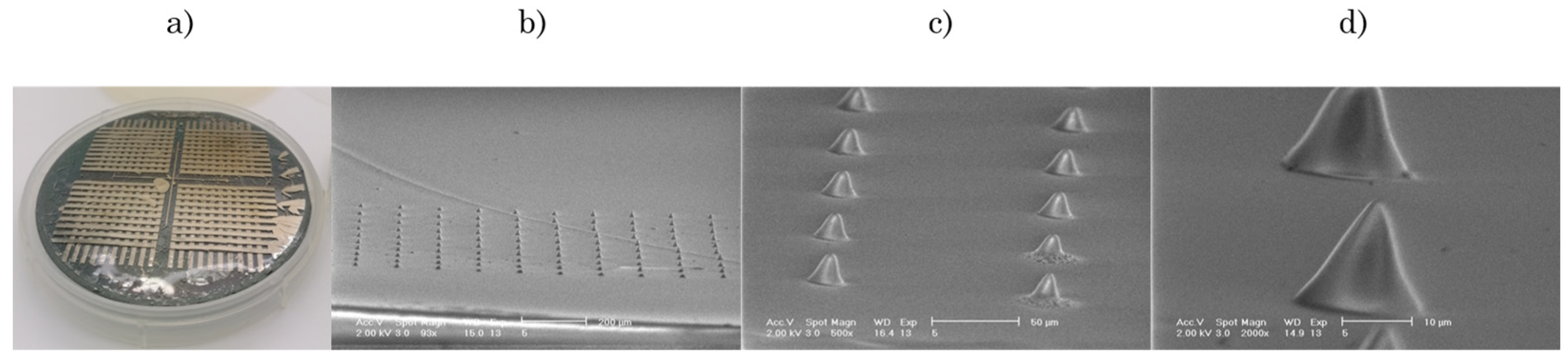
Figure 2a shows the fabricated Si wafer with four 10 × 10 row–column array sensors. In this design, the micro-cones of the active layer are situated in the electrode intersections, limiting the crosstalk effect and allowing for spatial pressure recognition. In Figure 2b–d, it is possible to observe the SEM images of the fabricated conical PDMS structures. When compared with previous studies (Table S1), the monolithic approach combined with the use of a sacrificial photosensitive molding layer proposed in this work allows for better layer uniformity. With this method, by bypassing the need for bonding steps, we can simultaneously miniaturize the design and guarantee similar sensing performance within the devices. Additionally, by having control over the active layer structure, one can easily predict the sensor’s output through simulations. In this study, the theoretical nominal capacitance (Equation (S2)) was determined to be equal to 332 fF, whereas the average measured nominal capacitance of a singular sensor was 248 fF. Preliminary measurement results indicate the sensors’ sensitivity to be 2.3069 kPa−1 for sample 1 and 1.67691 kPa−1 for sample 2 (Figures S1 and S2). With this approach, scalability can be improved by adopting established techniques widespread in the industry, such as photolithography.
Supplementary Materials
The following supporting information can be downloaded at https://www.mdpi.com/article/10.3390/proceedings2024097105/s1. Table S1. Comparison between recent studies; Equation (S1). Parallel-plate capacitance; Equation (S2): Nominal capacitance of a microstructured pressure sensor; Equation (S3). Occupied volume of the microstructured active layer; and Equation (S4). Distance between the electrode plates. Figure S1. Load (red) and unload (blue) capacitance of sample 1 (left) and sample 2 (right); Figure S2. Sample 1 capacitance change (left) with sensitivity of 2.3069 kPa−1. Sample 2 capacitance change (right) with sensitivity of 1.67691 kPa−1. References [1,4,5,6,7,8] are cited in the supplementary materials.
Author Contributions
Conceptualization, methodology, investigation, and writing—original draft preparation, M.B.A.R.; writing—review and editing, supervision, project administration, and funding acquisition, M.K. All authors have read and agreed to the published version of the manuscript.
Funding
This research was funded by H2020-EIC-FETPROACT-2019 Project 951949—NANOSTACKS.
Institutional Review Board Statement
Not applicable.
Informed Consent Statement
Not applicable.
Data Availability Statement
Data is stored on the department’s local server and can be made available on demand.
Conflicts of Interest
The authors declare no conflicts of interest.
References
- Luo, Y.; Shao, J.; Chen, S.; Chen, X.; Tian, H.; Li, X.; Wang, L.; Wang, D.; Lu, B. Flexible Capacitive Pressure Sensor Enhanced by Tilted Micropillar Arrays. ACS Appl. Mater. Interfaces 2019, 11, 17796–17803. [Google Scholar] [CrossRef] [PubMed]
- Gao, Y.; Xiao, T.; Li, Q.; Chen, Y.; Qiu, X.; Liu, J.; Bian, Y.; Xuan, F. Flexible microstructured pressure sensors: Design, fabrication and applications. Nanotechnology 2022, 33, 322002. [Google Scholar] [CrossRef] [PubMed]
- Ruth, S.R.A.; Feig, V.R.; Tran, H.; Bao, Z. Microengineering Pressure Sensor Active Layers for Improved Performance. Adv. Funct. Mater. 2020, 30, 2003491. [Google Scholar] [CrossRef]
- Peng, S.; Blanloeuil, P.; Wu, S.; Wang, C.H. Rational Design of Ultrasensitive Pressure Sensors by Tailoring Microscopic Features. Adv. Mater. Interfaces 2018, 5, 1800403. [Google Scholar] [CrossRef]
- Kwon, D.; Lee, T.-I.; Shim, J.; Ryu, S.; Kim, M.S.; Kim, S.; Kim, T.-S.; Park, I. Highly Sensitive, Flexible, and Wearable Pressure Sensor Based on a Giant Piezocapacitive Effect of Three-Dimensional Microporous Elastomeric Dielectric Layer. ACS Appl. Mater. Interfaces 2016, 8, 16922–16931. [Google Scholar] [CrossRef] [PubMed]
- Lee, Y.; Myoung, J.; Cho, S.; Park, J.; Kim, J.; Lee, H.; Lee, Y.; Lee, S.; Baig, C.; Ko, H. Bioinspired Gradient Conductivity and Stiffness for Ultrasensitive Electronic Skins. ACS Nano 2021, 15, 1795–1804. [Google Scholar] [CrossRef] [PubMed]
- Luo, Z.; Chen, J.; Zhu, Z.; Li, L.; Su, Y.; Tang, W.; Omisore, O.M.; Wang, L.; Li, H. High-Resolution and High-Sensitivity Flexible Capacitive Pressure Sensors Enhanced by a Transferable Electrode Array and a Micropillar-PVDF Film. ACS Appl. Mater. Interfaces 2021, 13, 7635–7649. [Google Scholar] [CrossRef]
- Zhang, W.; Sun, W.; Xiao, W.; Zhong, X.; Wu, C.; Guo, W. Numerical Simulation Analysis of Microstructure of Dielectric Layers in Capacitive Pressure Sensors. IEEE Sens. J. 2019, 19, 3260–3266. [Google Scholar] [CrossRef]
Figure 1.
Proposed fabrication process for the flexible pressure sensor: (a) Si carrier wafer; (b) deposition of PDMS bottom substrate; (c) deposition of bottom Ti/Pt/Ti electrode; (d) deposition of PDMS lamination layer; (e) deposition and patterning of the sacrificial molding layer; (f) deposition and molding of the active layer; (g) deposition of top Ti/Pt/Ti electrode and sacrificial layer etching; and (h) deposition of top PDMS substrate.

Figure 2.
(a) Fabricated row–column flexible pressure sensor; (b) SEM image of the active layer with 150× magnification; (c) SEM image of the active layer with 500× magnification; and (d) SEM image of the conical shape obtained with 2000× magnification.
Figure 2.
(a) Fabricated row–column flexible pressure sensor; (b) SEM image of the active layer with 150× magnification; (c) SEM image of the active layer with 500× magnification; and (d) SEM image of the conical shape obtained with 2000× magnification.
Disclaimer/Publisher’s Note: The statements, opinions and data contained in all publications are solely those of the individual author(s) and contributor(s) and not of MDPI and/or the editor(s). MDPI and/or the editor(s) disclaim responsibility for any injury to people or property resulting from any ideas, methods, instructions or products referred to in the content. |
© 2024 by the authors. Licensee MDPI, Basel, Switzerland. This article is an open access article distributed under the terms and conditions of the Creative Commons Attribution (CC BY) license (https://creativecommons.org/licenses/by/4.0/).
Share and Cite
MDPI and ACS Style
Rosa, M.B.A.; Kraft, M. Microengineered Flexible Pressure Sensors with Sacrificial Molding Layer: A Novel Fabrication Approach for Improved Performance. Proceedings 2024, 97, 105. https://doi.org/10.3390/proceedings2024097105
AMA Style
Rosa MBA, Kraft M. Microengineered Flexible Pressure Sensors with Sacrificial Molding Layer: A Novel Fabrication Approach for Improved Performance. Proceedings. 2024; 97(1):105. https://doi.org/10.3390/proceedings2024097105
Chicago/Turabian StyleRosa, Maria Brites Atalaia, and Michael Kraft. 2024. "Microengineered Flexible Pressure Sensors with Sacrificial Molding Layer: A Novel Fabrication Approach for Improved Performance" Proceedings 97, no. 1: 105. https://doi.org/10.3390/proceedings2024097105