


Abstract
Bulk piezoelectric ultrasound transducers on integrated circuits offer unique properties for therapeutic applications of ultrasound neuromodulation. However, current implementations of such transducers are not optimized for the high transmit efficiency required to stimulate neurons. This is mainly due to the challenge of implementing a metal layer on top of the piezoelectric film using microfabrication techniques. Here, we propose a micromachined capping structure providing an electrical connection on top of the piezoelectric film with minimal acoustic losses. The structure can potentially be used as a common ground connection in phased-array ultrasound transducers.
1. Introduction
Therapeutic neuromodulation is a promising biomedical application of focused ultrasound which, compared to imaging, introduces design emphasis on high transmit efficiency and small form factor [1]. Bulk piezoelectric transducers afford higher transmit efficiency than conventional micromachined ultrasound transducers [2]. However, the integration of bulk piezoelectric film on integrated circuits (ICs) using microfabrication techniques is challenging due to the film thickness. This is especially the case when considering a shared ground terminal connection to the top of the film. Current implementations of such a top connection introduce acoustic losses detrimental to the output pressure of the transducer [3]. To overcome these challenges, we propose a microfabricated conductive membrane suspended on a silicon frame as top-level electrical connection to the piezoelectric transducer. The thickness of the frame can be matched to that of various piezoelectric films.
2. Materials and Methods
The conductive membrane consists of a thin, sputtered Al(1%Si)/Ti layer supported by a polydimethylsiloxane (PDMS) layer. PDMS was chosen by virtue of its mechanical flexibility and suitable acoustic properties, matching those of soft tissues.
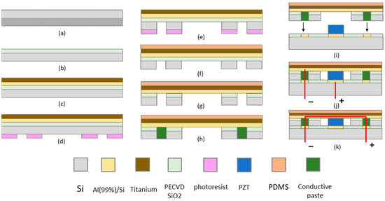
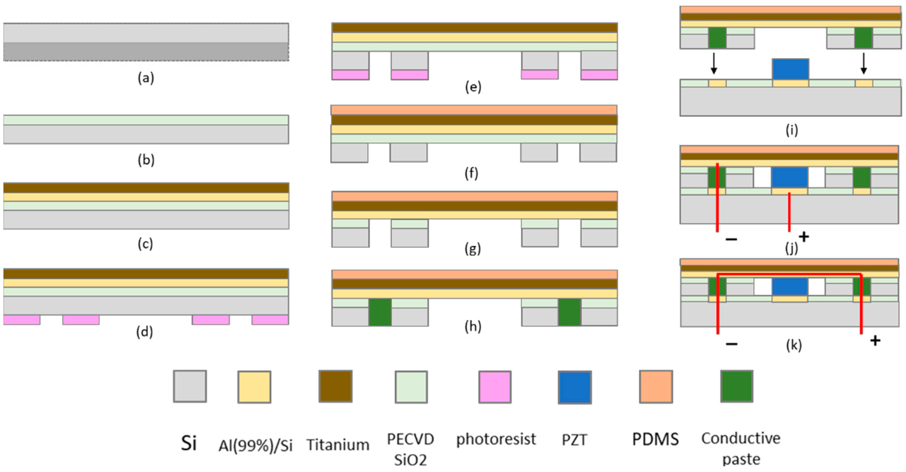
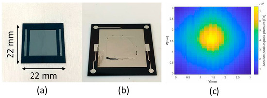
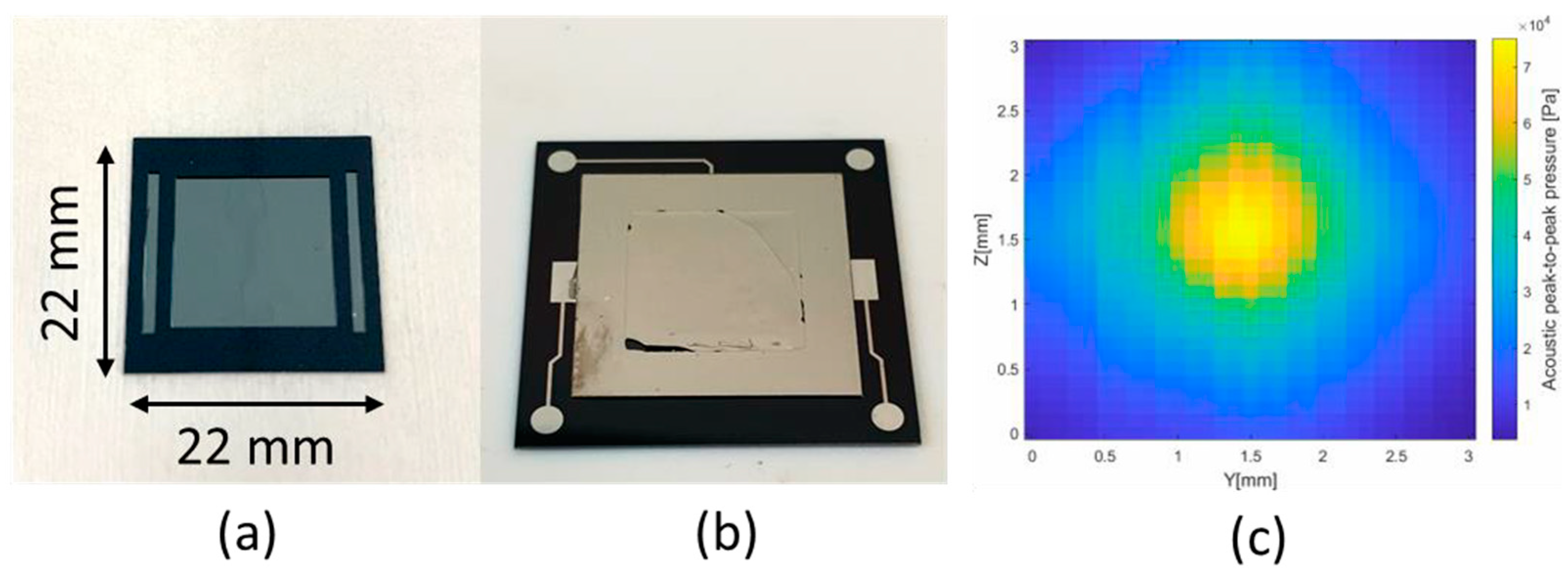
Figure 1 depicts the fabrication process of the cap structure, which starts with thinning down a double-side polished 300 µm-thick silicon wafer to match the thickness of the desired piezoelectric film using deep reactive ion etching (DRIE). Next, a 4 µm-thick PECVD silicon dioxide layer was deposited on the front side of the wafer, followed by the sputtering of a 400/40 nm-thick aluminum/titanium layer. Using DRIE, the silicon was etched from the back until landing on the silicon dioxide, creating the membrane and contact openings. Then, PDMS was spin-coated and cured on the aluminum layer. The oxide layer was removed by using buffered HF (1:7), and the wafer was diced (Figure 2a). The contact openings were filled with conductive paste to create conductive vias through the silicon frame. Finally, the cap structure was mounted onto the existing ground pad of an IC, with the membrane in contact with the top of the piezoelectric layer, as shown in Figure 2b.
Figure 1.
Fabrication and assembly of the capping structure. (a) Thinning down of silicon wafer to match the piezoelectric film thickness. (b) Deposition of PECVD SiO2. (c) Sputtering of Al(1%Si) and Ti. (d) Backside patterning of positive photoresist (AZ 12XT-20PL). (e) Backside DRIE of the Si wafer. (f) Spin-coating of PDMS on the front side of the wafer. (g) Etching of SiO2 using BHF (1:7). (h) Filling of the contact groove with conductive paste. (i) Assembly of the top-level connection on a test chip. Lead zirconate titanate (PZT) was used as piezoelectric material. (j) Terminal configuration to drive the transducer. (k) Terminal configuration to measure the electric resistance of the membrane.
Figure 2.
(a) Bottom-view of the proposed cap structure, (b) cap structure assembled on top of a test chip with PZT. (c) Measured pressure profile of the assembled transducer (focal distance: 10 mm).
3. Results and Discussion
The integrated system showed good performance. The resistance measured across the Al/Ti/PDMS membrane was 5.7 Ω, which introduced a voltage drop of only 0.05 V at the operating current with 10 V driving voltage. Preliminary results prove that the proposed cap structure can provide an effective electrical connection to the piezoelectric film, generating a clear ultrasound signal as recorded using a hydrophone (Figure 2c). Further testing and optimization will be conducted to tune the output pressure and characterize different thicknesses of PZT for different ultrasound frequencies.
Author Contributions
G.K.W. conceived the idea, designed and performed the experiments; G.K.W., T.L.C. and M.M. validated the results; T.L.C. and M.M. supervised the project; G.K.W., T.L.C. and M.M. administered the project; G.K.W. wrote the original draft; T.L.C. and M.M. reviewed and edited the article; M.M. secured funding. All authors have read and agreed to the published version of the manuscript.
Funding
This research received no external funding.
Institutional Review Board Statement
Not applicable.
Informed Consent Statement
Not applicable.
Data Availability Statement
Not applicable.
Conflicts of Interest
The authors declare no conflicts of interest.
References
- Pashaei, V.; Dehghanzadeh, P.; Enwia, G.; Bayat, M.; Majerus, S.J.; Mandal, S. Flexible Body-Conformal Ultrasound Patches for Image-Guided Neuromodulation. IEEE Trans. Biomed. Circuits Syst. 2020, 14, 305–318. [Google Scholar] [CrossRef] [Scilit] [PubMed]
- Dew, E.B.; Ilkhechi, A.K.; Maadi, M.; Haven, N.J.; Zemp, R.J. Outperforming piezoelectric ultrasonics with high-reliability single-membrane CMUT array elements. Microsyst. Nanoeng. 2022, 8, 59. [Google Scholar] [CrossRef] [Scilit] [PubMed]
- Costa, T.; Shi, C.; Tien, K.; Elloian, J.; Cardoso, F.A.; Shepard, K.L. An Integrated 2D Ultrasound Phased Array Transmitter in CMOS With Pixel Pitch-Matched Beamforming. IEEE Trans. Biomed. Circuits Syst. 2021, 15, 731–742. [Google Scholar] [CrossRef] [Scilit] [PubMed]
Disclaimer/Publisher’s Note: The statements, opinions and data contained in all publications are solely those of the individual author(s) and contributor(s) and not of MDPI and/or the editor(s). MDPI and/or the editor(s) disclaim responsibility for any injury to people or property resulting from any ideas, methods, instructions or products referred to in the content. |
© 2024 by the authors. Licensee MDPI, Basel, Switzerland. This article is an open access article distributed under the terms and conditions of the Creative Commons Attribution (CC BY) license (https://creativecommons.org/licenses/by/4.0/).