
Research by Fondazione Bruno Kessler on Strategies to Improve the Yield in Plasma Focused Ion Beam Circuit Editing †


MNF—Micro Nano Facility, Center for Sensors & Devices—Fondazione Bruno Kessler, I-38123 Trento, Italy
*
Authors to whom correspondence should be addressed.
†
Presented at the XXXV EUROSENSORS Conference, Lecce, Italy, 10–13 September 2023.
Proceedings 2024, 97(1), 59; https://doi.org/10.3390/proceedings2024097059
Published: 20 March 2024
Abstract
:This contribution explores the potential of PFIB for the post-production circuit editing of custom ASICs. The reworking of integrated circuits with ion beam is an effective tool for testing design modifications rapidly, and in small-volume productions, it proves to be a valuable substitute for the microfabrication of chips with a revised layout, thus reducing the cost and lead time. In the case study in this work, the PFIB intervention resulted in the recovery of ~90% of defective channels in a multichannel ASIC design by disconnecting some parts of the internal circuit. This contribution describes several implemented optimization strategies and their statistical effectiveness.
1. Introduction
The last generation of Xe PFIB (plasma-focused ion beam) has emerged as a tool of significant value for clean-room facilities due to its versatility in the circuit editing, wafer-level inspection, and failure analysis of fully packaged integrated circuits [1,2]. With an upgrade granted by an IPCEI project, the FBK research institute has added advanced PFIB-SEM capabilities to support clean-room engineers [3]. In this work, we aimed to explore the potential of this technique for circuit editing on a statistically relevant number of ASICs with intrinsic production defects affecting the chips’ performance.
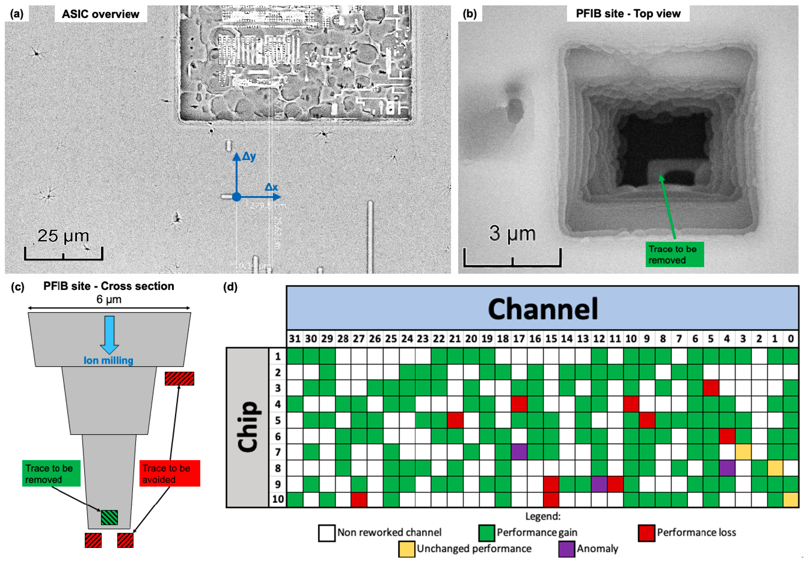
In this study, we used a dedicated test bench to evaluate the chips’ performance before and after reworking. We performed a comprehensive analysis of various strategies to the minimize collateral damage from PFIB process. The first challenge is the minimization of defects (e.g., through discharge) on logic blocks in the circuit. The second task is to avoid damage to neighboring structures that are very close but outside of the milling volume; thus, good alignment and careful design in the milling crater are paramount (as described in Figure 1a,c) as the layout is comprised of several metal layers.
Finally, process optimizations [4] helped to identify the most suitable milling recipe for a fast process and for the reworking of hundreds of channels. From the first batches of ASICs to the final batch results presented here, the yield was drastically improved, despite some failed reworking instances, mostly due to discharges, not being eliminated as they are intrinsic to the ionic milling process of the insulator in proximity of buried logic blocks. Overall, the experimental results for the functional testing demonstrate the effectiveness of the PFIB reworking.
2. Materials and Methods
The multichannel ASICs, consisting of 32 identical channels used for the back-end signal processing of FBK’s detectors, were functionally tested, revealing a very high percentage of non-functioning channels (>50%). Multiple attempts were made to rework the chips with ion beams to analyze the origins of the problem and define possible strategies for the circuit’s modification before a new production run. A dedicated test setup was created, allowing the evaluation of the performance of the chips on the go, giving instant feedback to the PFIB intervention. The most promising strategy to restore the channel’s functionality was disconnecting a certain part of the internal circuit by removing a buried metal trace, which is most compatible with FIB reworking. A Xe Plasma FIB-SEM Helios 5 from Thermo Fisher Scientific (Waltham, MA, USA) was used at 30 kV with a 4 nA ion beam. All channels were tested after the FIB operations to access the performance gains in the reworked channels or also possible damage or anomalies in the non-reworked channels.
3. Discussion
ASICs comprising 32 channels were used in this analysis. In the ASICs used, the initial average number of fully operational channels was only 48%, and, as shown in Figure 1d, their distribution was unpredictable among the batch of chips tested (additionally confirmed via measurements of another 20+ chips that were yet to be subjected to the reworking). This is speculated to be caused by the design tolerances in complex multi-metal layer stacks such as ASIC that can have a high impact on channel-specific performance. Fault diagnosis was carried out to identify a PFIB reworking procedure for the remaining 52% of the channels. A two-step optimization process for the milling recipe was carried out. Firstly, the milling recipes were tuned to achieve the right depth in the area of interest while minimizing the milling volume and interference with adjacent structures. Secondly, the speed of the operation was optimized, as it represented a balance between time (i.e., the ion beam current, which can typically be changed in increments of 4 times as it is linked to physical apertures) and clean vertical walls (i.e., lower material re-sputtering). This optimization brought some fine nuances to the PFIB process for the design milling crater in Figure 1c, and its final results are depicted in Figure 1d. The overall performance recovery was significant, improving from below 50% to more than 90%.
Going forward, the high-precision and fast milling allowed by PFIB could prove an efficient alternative to avoid a new silicon run that could take 8–9 months and cost the ASICs of a small research production several tens of thousands of dollars.
Author Contributions
D.N. and E.D. contributed equally during all stages of the work, L.F. contributed to writing—review and editing, and supervision. All authors have read and agreed to the published version of the manuscript.
Funding
D.N. was supported by Caritro Foundation for the funding of young researchers. Grant name: FlexBond.
Institutional Review Board Statement
Not applicable.
Informed Consent Statement
Not applicable.
Data Availability Statement
Access to data can be provided upon request.
Conflicts of Interest
The authors declare no conflicts of interest.
References
- Liu, T.C.; Chen, C.; Liu, S.T.; Chang, M.L.; Lin, J. Innovative methodologies of circuit edit by focused ion beam (FIB) on wafer-level chip- scale-package (WLCSP) devices. J. Mater. Sci. Mater. Electron. 2011, 22, 1536–1541. [Google Scholar] [CrossRef]
- Chen, L.; Longoria, A.; Cha, G.; Tovar, G.; Ramirez, E.; Fang, P.; Liu, Y.; Torres, A.; Alcantara, M.; Penley, C. Application of Plasma Focused Ion Beam Technique in Advanced Technology Nodes. In International Symposium for Testing and Failure Analysis; ASM International: Almere, The Netherlands, 2022. [Google Scholar]
- Novel, D.; Demenev, E.; Ferrario, L. PFIB capabilities and potential for circuit edit and 3D integration at FBK. In Proceedings of the 48th International conference on Micro and Nano Engineering—Eurosensors (MNE-ES), Leuven, Belgium, 19–23 September 2022. [Google Scholar]
- Gaiardo, A.; Novel, D.; Scattolo, E.; Crivellari, M.; Picciotto, A.; Ficorella, F.; Iacob, E.; Bucciarelli, A.; Petti, L.; Lugli, P.; et al. Optimization of a Low-Power Chemoresistive Gas Sensor: Predictive Thermal Modelling and Mechanical Failure Analysis. Sensors 2021, 21, 783. [Google Scholar] [CrossRef] [PubMed]
Figure 1.
(a) Large milling area milled with a high beam current. It was used as a reference to find relative coordinates from a surface morphology to the buried trace to be removed. (b) Top view of the crater after milling. The trace to be removed is highlighted. (c) Cross-section of the milling crater that was used to reach the deep metal layer to be removed. The positioning precision needs to be below 500 nm. (d) Map showing the yield in chips for 10 reworked chips.
Disclaimer/Publisher’s Note: The statements, opinions and data contained in all publications are solely those of the individual author(s) and contributor(s) and not of MDPI and/or the editor(s). MDPI and/or the editor(s) disclaim responsibility for any injury to people or property resulting from any ideas, methods, instructions or products referred to in the content. |
© 2024 by the authors. Licensee MDPI, Basel, Switzerland. This article is an open access article distributed under the terms and conditions of the Creative Commons Attribution (CC BY) license (https://creativecommons.org/licenses/by/4.0/).
Share and Cite
MDPI and ACS Style
Novel, D.; Demenev, E.; Ferrario, L. Research by Fondazione Bruno Kessler on Strategies to Improve the Yield in Plasma Focused Ion Beam Circuit Editing. Proceedings 2024, 97, 59. https://doi.org/10.3390/proceedings2024097059
AMA Style
Novel D, Demenev E, Ferrario L. Research by Fondazione Bruno Kessler on Strategies to Improve the Yield in Plasma Focused Ion Beam Circuit Editing. Proceedings. 2024; 97(1):59. https://doi.org/10.3390/proceedings2024097059
Chicago/Turabian StyleNovel, David, Evgeny Demenev, and Lorenza Ferrario. 2024. "Research by Fondazione Bruno Kessler on Strategies to Improve the Yield in Plasma Focused Ion Beam Circuit Editing" Proceedings 97, no. 1: 59. https://doi.org/10.3390/proceedings2024097059