An Overview on the Formation and Processing of Nitrogen-Vacancy Photonic Centers in Diamond by Ion Implantation

1
Department of Physics, Astronomy, and Materials Science, Missouri State University, Springfield, MO 65897, USA
2
Department of Electrical Engineering, Georgia Southern University, Statesboro, GA 30458, USA
*
Author to whom correspondence should be addressed.
J. Manuf. Mater. Process. 2017, 1(1), 6; https://doi.org/10.3390/jmmp1010006
Submission received: 24 July 2017
/
Revised: 12 August 2017
/
Accepted: 21 August 2017
/
Published: 25 August 2017
Abstract
:Nitrogen-vacancy (NV) in diamond possesses unique properties for the realization of novel quantum devices. Among the possibilities in the solid state, a NV defect center in diamond stands out for its robustness—its quantum state can be initialized, manipulated, and measured with high fidelity at room temperature. In this paper, we illustrated the formation kinetics of NV centers in diamond and their transformation from one charge state to another. The controlled scaling of diamond NV center-based quantum registers relies on the ability to position NV defect centers with high spatial resolution. Ion irradiation technique is widely used to control the spatial distribution of NV defect centers in diamond. This is addressed in terms of energetics and kinetics in this paper. We also highlighted important factors, such as ion struggling, ion channeling, and surface charging, etc. These factors should be considered while implanting energetic nitrogen ions on diamond. Based on observations of the microscopic structure after implantation, we further discussed post-annealing treatment to heal the damage produced during the ion irradiation process. This article shows that the ion implantation technique can be used more efficiently for controlled and efficient generation of NV color centers in diamond, which will open up new possibilities in the field of novel electronics and computational engineering, including the art of quantum cryptography, data science, and spintronics.
1. Introduction
For many years, scientists have been looking for ideal candidates to use as information carriers qubits for quantum computation and communications [1,2,3]. Spins associated with defects in diamond have shown good promise for those purposes [4]. The ideal platform to be used for quantum-age technologies is the nano-patterned diamond, especially when the scientific community is able to achieve electron-spin operation in some particular types of defect like color centers in diamond. Among them, the nitrogen-vacancy (NV) color centers become the most promising candidates because they exhibit atom-like properties, such as long-lived spin quantum states and a well-defined optical transition in solid state devices [5]. These kinds of point defects are also promising for a number of applications such as quantum state engineering [6], and magnetic sensors [7]. Coupling those point defects with a number of systems to achieve scalability and a single shot readout is also very important [8,9]. NV centers in diamond are among the most interesting objects for producing quantum elements that fulfill the well-established Di Vincenzo’s criteria for quantum information technology at room temperature [10]. However, the distribution of grown NV centers at diamond is random. This causes great difficulties in photon-NV center coupling, which is a perquisite for any kind of practical application based on quantum mechanical theory. Therefore, it is indispensable to generate artificial NV centers in diamond lattices in a controlled way [11]. In particular, creating patterned NV centers or a 2-dimensional array of NV centers at specific positions maintaining a minimum distance in the diamond matrix is highly preferable for recording and storing quantum information and transmitting that information in the form of light. Ion implantation is the best way to spatially control the positions at which such a color center should be created or embedded. Meanwhile, ion implantation techniques have kept improving both in terms of spatial resolution of implantation (almost at the nanometer level) and in control of the number of implanted ions (aiming at the deterministic implantation of single ions) [12,13]. Furthermore, because the ion implantation process can be integrated with lithography, it will be possible to implant a single NV color center or NV optical centers in a designed form with other structures such as microcavities, nano-photonics, and micro-circuits on a chip. However, ion implantation is only the first step toward the creation of quantum devices based on NV centers in diamond. There is a considerable lag in collective approaches with respect to the overall production kinematics of NV centers by ion implantation technique, identifying the hidden problems behind the slow progress in obtaining high quality NV color centers in diamond, and finding out proper solutions to eliminate those obstacles. For these reasons, we thoroughly studied the progress in this field, identified the technological impediments and proposed some indigenous solutions.
In the first part of this article we describe the general formation procedure of NV centers and their energetics. In the next part, we discuss the production of NV centers by ion irradiation, issues that affect the irradiation process, and post-annealing treatment to compensate the irradiation-induced defects. At the end of this article, we briefly highlight the factors to be considered during the ion implantation of diamond, providing a general discussion and concluding remarks. We also suggested some of the improvement strategies for obtaining high quality NV centers in diamond by ion implantation for efficient devices.
2. General Overview of the NV Center
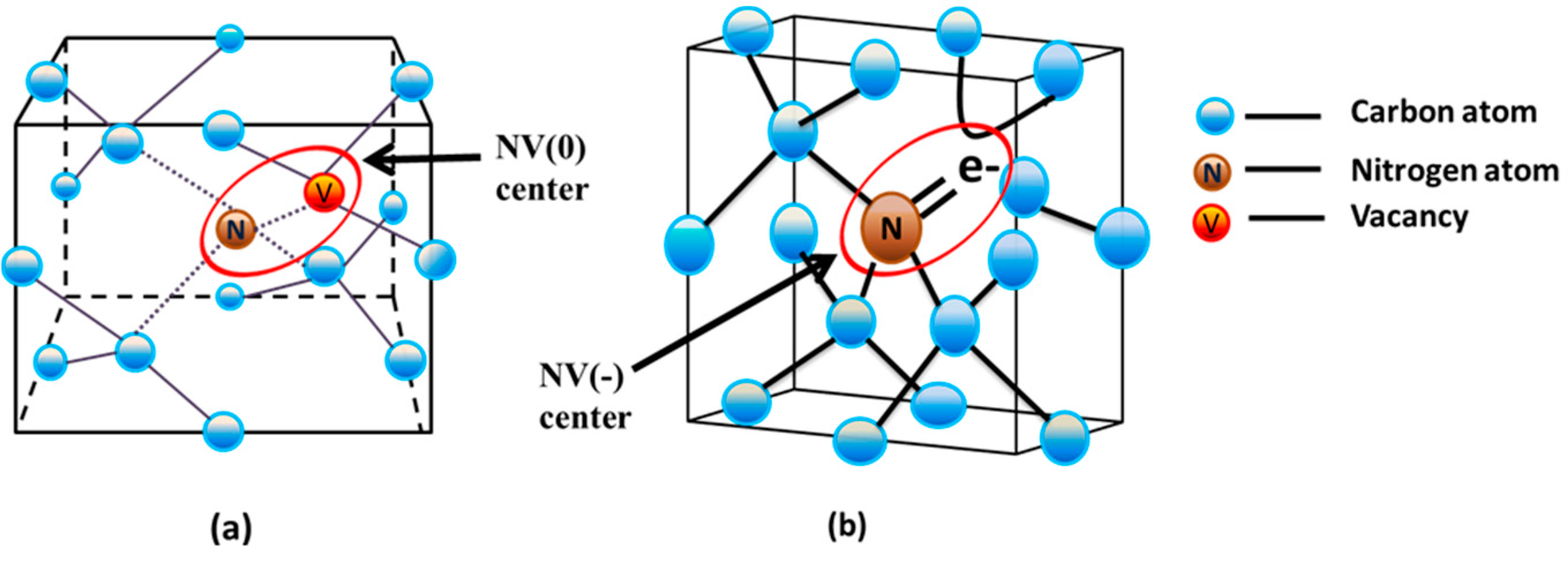
Among numerous point defects in diamond, the NV center is the most studied and scientifically the most promising for nano-photonics and quantum computing applications. It consists of a substitutional nitrogen (N) atom coupled with a vacancy (V) in one of its eight nearest neighboring sites of the diamond crystal lattice. As soon as a substitutional N atom couples with a vacancy, three electrons of the N atom link with the three neighboring C atoms to form covalent bonds and the remaining two electrons form a lone pair. The NV center shows C3v symmetry, meaning it has a 120° symmetrical rotation along the N and V bond axis. The NV center has a general tendency to trap an additional electron from the negatively charged center, denoted as NV(−). Figure 1a represents the presence of an NV(0) center in a diamond unit cell and Figure 1b shows its conversion into NV(−). Figure 2a represents the ground and excited energy levels in both of the charge states of this defect. In photoluminescence spectroscopy the NV photonic center absorbs green light and emits radiations at 2.156 eV and 1.945 eV associated with NV(0) and NV(−) color centers, respectively [14]. Figure 2b represents the corresponding luminescence spectra [15].
An NV center is very useful because of the ease of its photoluminescence detection, and the electron spin of such kind of centers can be tuned by applying and changing an electric field, magnetic field, electromagnetic radiation, or a combination [16]. In particular, the NV(−) color center consists of roughly a dozen sharp lines in the optical spectra with a separation in the megahertz to gigahertz range, which can be resolved by proper sample preparation. The relative intensity and positions of those optical lines can be engineered by a number of procedures, which can provide extra advantages during the logic-based device design or operation of the NV center-based practical device. These procedures can be summarized as follows. Firstly, the amplitude and the orientation of the applied magnetic field splits the sub-levels in the ground and excited energy states. Secondly, the continuous microwave radiation changes the population of the sub-bands within both of the energy states [17]. Thirdly, application of the tunable lasers can selectively excite certain sub-levels in both ground and excited energy states [17,18]. Fourthly, by tuning the amplitude and direction of the applied electric field one can effectively control the sub-level splitting [17]. Fifthly, a similar approach can be induced by changing the amplitude and orientation of the elastic strain (mechanical strain) onto the diamond structure [19]. Finally, in addition to those static perturbation effects, one can utilize several other dynamic functions, such as Rabi oscillations, spin echo, etc. by employing a thoughtful designed/engineered sequence of microwave pulses [20,21,22].
Typically, the NV centers are randomly positioned and oriented in a natural diamond lattice. However, they can be artificially created in an oriented manner at predetermined positions by ion implantation technique. In the next section we will discuss on the formation of NV color centers in a diamond lattice from the thermodynamic point of view.
3. The Formation of NV Centers
NV centers are produced in large area single crystal diamond as well as in nano-diamonds by ion implantation technique [24]. However, during ion implantation, it is easier to induce structural modifications (graphitization) in diamond nanoparticles compared to the large area single crystal diamond thin film [25]. To understand the formation mechanism of NV photonic centers such as NV(0) and NV(−) color centers in diamond, it is important to understand details about the formation of the substitutional nitrogen defect and single vacancy defect, which are described below in Section 3.1.
3.1. Formation of Substitutional Nitrogen (Ns)
Ns is the most prominent and thoroughly studied defect of natural as well as N-doped synthetic diamonds. It is stable up to a very high temperature (2100 °C) with a high diffusion activation energy of ~5.0 ± 0.3 eV. However, this activation energy can be lowered up to 2.6 eV using the assistance of pressure-generated intrinsic defects [26]. For the direct interexchange of Ns with a neighbor C atom in the diamond matrix, the theoretical activation energy is ~6.3 eV at 0 K temperature [27]. On the other hand, the rate-limiting step was calculated as 4.8 eV for vacancy-assisted diffusion, i.e., the jump of Ns into a next neighbor vacancy (V) [28]. The Ns point defect is also optically sensitive. In UV absorption, the A band at 3.3 eV and the B band at 3.9 eV are assigned to vertical transitions from the A1 ground state of the defect to effective-mass-like A1 and E excited states, respectively. A negatively charged state of Ns referred as Ns(−) is also existent. Local density approximation (LDA) calculations show Ns has C3v symmetry with the distance of Ns to the nearest C-neighbor along the trigonal axis being ~28% longer than the usual C–C bond distance [26].
3.2. The Single Vacancy (V)
The single vacancy is another very common point defect in diamond, which is the origin of numerous bands in the optical spectra of diamond. It may also exist as charged state V(−). At room temperature V(0) is mobile and at elevated temperature region (between 600 and 800 °C) V(0) is mobile with an activation energy of 2.3 ± 0.3 eV [29]. On the other hand, V(−) is immobile and this type of vacancy undergoes a charge transition before any diffusion phenomena.
3.3. The Nitrogen-Vacancy (NV) Center
The NV center is a point defect in the diamond lattice. It is formed by a substitution nitrogen atom and an adjacent lattice vacancy. Out of the five valance electrons of the N atom, three of them form covalent bonds with the neighboring C atoms. The remaining two non-bonded electrons are called a lone pair. On the other hand, a lattice vacancy consists of three unpaired electrons, of which two form a quasi-covalent bond and the third one remains unpaired. As described earlier, the overall symmetry of a NV center is axial with trigonal pyramidal configuration (C3v) where these three unpaired electrons continuously interchange their positions. The only truly unpaired electron (the third electron of the vacancy site) is mainly responsible for the paramagnetic characteristics in the N−V(0) center. In case of the negatively charged NV(−) center, the vacancy site holds an extra electron and thereby forms a spin pair with the third vacancy electron. This extra electron comes from the lattice (nitrogen donors). The electron density is mainly located in a plane vertical to the main NV axis. The highest density of electrons is on the three carbon atoms and the vacant site. The neutral charge state of NV center, NV(0), and positively charged state, NV(+), are magneto-optically inactive. Therefore, virtually all the experiments are carried out on NV(−) color centers. An NV(2−) charge state could in principle also exist, but donors shallower than the Ns would be needed to obtain them. The nitrogen to vacancy (N→V) jump is a critical step for the diffusion of these NV centers. A high barrier height of 4.5 eV implies that NV centers are immobile at room temperature or even up to a certain elevated temperature [30]. Calculation shows that the mobilization begins above 1700 °C [31].
From study of nitrogen doped diamond at equilibrium, it is known that nitrogen impurities do not aggregate when the concentration of nitrogen during the growth process is below a certain level, i.e., less than 500 ppm for CVD-grown diamond. Above 2000 K the equilibrium state breaks down and the nitrogen atoms may aggregate to form N(−2) defects. More often, the growth temperature and heat treatment temperature of diamond are below this temperature. Therefore, the possibility of the formation of N2 and N2V defect states in the diamond lattice can be excluded [32]. The nitrogen concentration present in the diamond structure depends on several growth conditions such as temperature, pressure, any possible source of nitrogen in the form of precursors, plasma or processing gas etc. From theoretical calculations it is evident that defects such as Ns, V, NV, and V2 are formed during heat treatment at around 1100 K [29]. Usually during the growth process of diamond V and V2 do not form due to their high formation energies. Studies showed that under the abovementioned heat treatment condition the [Ns]/[NV] ratio is around 1000, which means concentration of NV defect centers is only 0.1% of the Ns concentration. As a consequence, only 0.1% of the Ns defects need to donate an electron to the NV centers to completely convert them into NV(−) [29]. These observations are done only at the bulk regions. However, the surface energetics causes the NV(−) to convert into NV(0) [33].
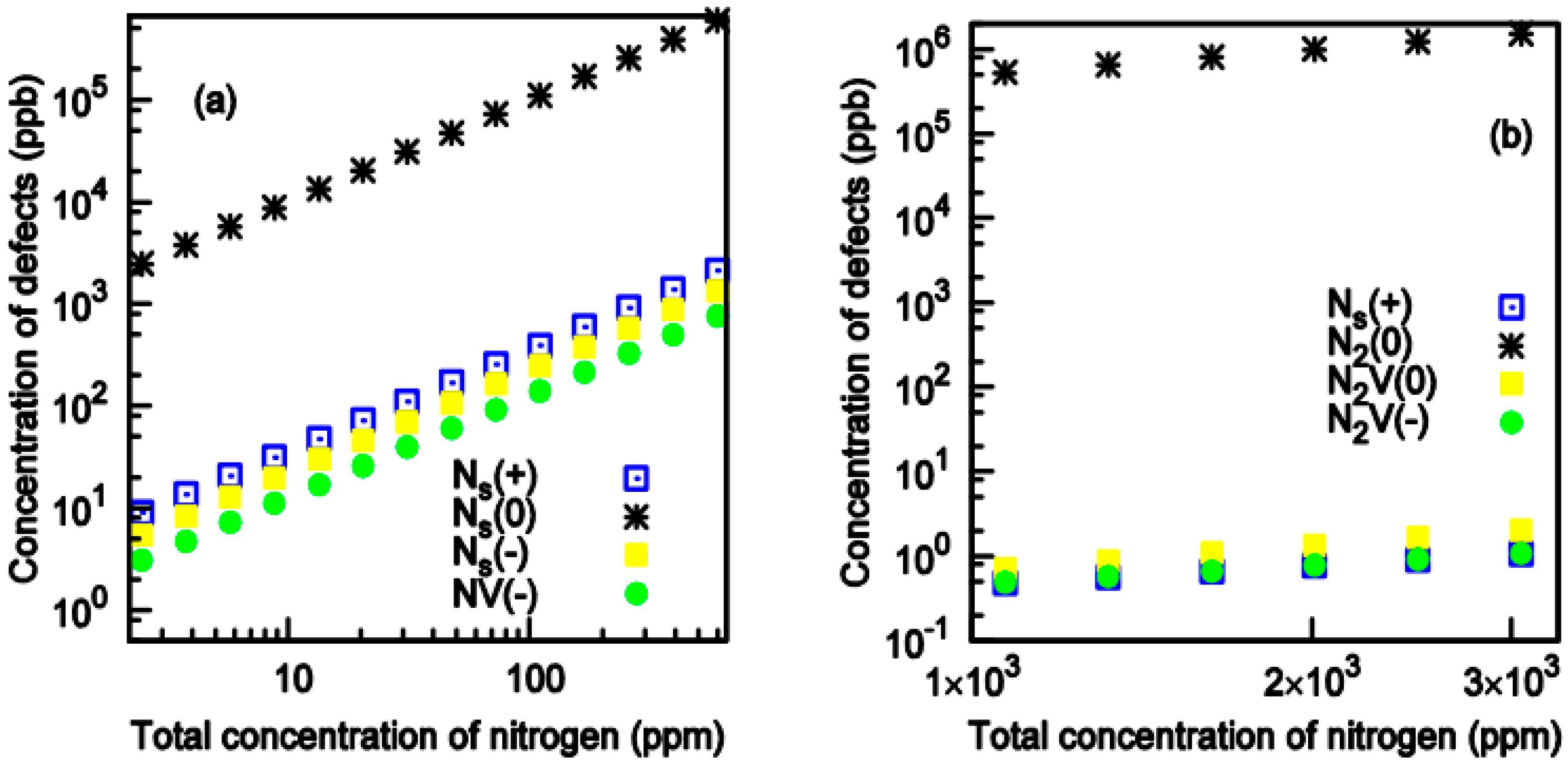
On the other hand, when the nitrogen concentration during the growth process is high, i.e., between 1000 and 3000 ppm for CVD-grown diamond, the mean distance between nitrogen impurities is few lattice constants. Therefore, at relatively low temperature, i.e., ~1100 K, they may aggregate and form N2 and N2V. Mostly these N2 defects remain in the form of N2(0), at zero charge state, and a very small fraction (~1 ppb) of N2 can capture V to convert into N2V. Under these conditions the NV concentration is negligible. Deák et al. calculated the concentration of different types of defects in diamond matrix after high temperature annealing at 1100 K, which is shown in Figure 3 [29].
4. Energetics to Produce NV Centers
In 2005 Goss et al. modeled a large range of impurity systems, where they showed a large number of dopants (X) may capture vacancies to produce dopant-vacancy such as NV centers [34]. On the calculation of the binding energies of the dopant-vacancy (XV) complexes some important conditions have been identified using the following reaction.
X + V → XV
- (1)
- The XV point defect is stable or bound if the formation energy (enthalpy) of XV center, EXV, is less than that of X (EX) and V (EV). Therefore, EXV < EX + EV.
- (2)
- If the energy required to displace a carbon from the lattice site in the diamond is EC, then the defect complex XV is likely to form, provided EXV + EC < EX.
- (3)
- If the energy of the displaced interstitial carbon is EI (~12 eV), then the XV complex will not be formed unless EXV + EI < EX.
While establishing these conditions it was considered that no dopant-vacancy complex has shallow electronic levels. All the calculations were done at 0 K temperatures and therefore in most of the entropic considerations were neglected. All the conditions are also valid for charged species/dopants and defects.
5. NV Centers Produced by Ion Irradiation and Subsequent Annealing
Ion implantation is a good technique to control the spatial distribution of dopants in the semiconductor industry, especially when the device dimension is smaller than micrometers. By ion irradiation and subsequent annealing the concentration of NV(−) photonic centers can be increased. The high energy ion irradiation creates Frankel pairs as well as other damage in the diamond lattice [35]. Annealing provides energy for the mobilization of those defects, but some of those Frenkel pairs may split and produce isolated vacancies and self-interstitials and follow arbitrary direction of motion. The concentration of these isolated vacancies and self-interstitials is very large compared to non-irradiated samples.
The self-interstitials are mobile even at room temperature and will aggregate to the surface or grain boundaries, or form platelet-like defects. In the meantime they can assist nitrogen diffusion and aggregation, too. Subsequent to irradiation, a heat treatment is required to anneal out luminescence-quenching parasitic defects. This is usually done at between 600 °C and 800 °C, where neutral vacancies become mobile. It is usually assumed that NV centers are formed during this heat treatment when vacancies get trapped at Ns defects. However, vacancies may also get trapped at existing N2 defects, or can form divacancies. The post-irradiation annealing can be regarded as a quasi-equilibrium process, and an insight into the creation of NV(−) centers can be gained by close inspection of the formation energies and occupation levels of the considered defects. In order to have mobile, i.e., neutral vacancies after the irradiation, the Fermi-level must be lowered drastically; below the single acceptor level of V (at about EV + 2.0 eV). Thus, if NV defects are to be created by irradiation and annealing, the vacancy concentration should be in excess of the Ns concentration ([V] > [Ns]), even after the trivial recombination with interstitials [36]. Then, two basic exothermic reactions can occur, which are described by the following equations.
where h denotes hole and its energy level corresponds to the given Fermi-level position. At [V] > [Ns], Equation (1) provides a higher energy gain than Equation (2). Hence the majority of the vacancies will form divacancies and only a small fraction creates NV defects. In fact, since the formation of V2 is about 0.9 eV more than that of NV, the equilibrium concentration of V2 will be several orders of magnitude larger than that of NV, even at relatively high temperatures. This implies that the concentration of NV defects will not significantly rise without irradiation. As isolated vacancies start to form V2 and NV defects, the Fermi-level shifts towards a higher energy side because both V2 and NV are deeper acceptors than V. As a result, the remaining isolated vacancies will become negatively charged and immobilized. Hence, from this study we can infer that after a certain level an increase in the vacancy concentration cannot contribute to raising the concentration of NV centers also denoted as [NV].
V(0) + V(0) → V2(0) + 4.2 eV
V(0) + Ns(+) → NV(0) + h + 3.3 eV
Therefore, we can predict that the increase in the NV defect concentration occurs only when NV defects are dominantly formed during the irradiation process, whereas during annealing the probability of the formation of V2 is higher. The creation of a vacancy close to Ns defect requires an energy of 2.26 eV to form a NV(0) defect. The formation energy for a neutral vacancy site in the perfect lattice is very large (~7.14 eV). These reactions are expressed below.
where C is a carbon atom in the perfect diamond lattice.
Ns(0) + 2.26 eV → NV(0) + C
perfect lattice + 7.14 eV → V(0) + C
The abovementioned two defect-producing reactions can be explained—breakage of only three strong C–C bonds is required to remove a C atom associate with Ns, whereas four such bonds are needed to break in the ideal diamond matrix in order to form an isolated neutral vacancy, V(0). Such a big energy difference should lead to a strong preference for the formation of NV centers even in the non-equilibrium process of irradiation. Therefore, the dominant part of the NV concentration is created directly at the time of irradiation. The neutral NV centers may convert into negatively charged centers if a sufficient concentration of nitrogen is present in the system.
N0 + NV(0) = N+ + NV(−)
The reaction expressed by Equation (5) requires energy greater than 2.4 eV. This energy might be supplied by an external light source or some other electromagnetic radiation sources. Figure 4 describes the schematic of the generation of NV centers in diamond by ion irradiation and successive annealing.
6. Factors to Be considered during the Nitrogen Ion Implantation on Diamond
6.1. Ion Struggling
After having been accelerated, a high velocity N ion first hits the surface of the static diamond target, then propagates through the diamond lattice, and finally loses energy, being scattered several times until it stops and substitutes a C atom in the diamond lattice. This results in a broadening of the ion beam focus, which can be defined as the uncertainty in the final position of each single implanted ion. The scatterings can be due to collisions with the electrons or with the nucleus of the atoms. The collisions with the electrons reduce the velocity mainly, whereas collisions with the nuclei change the direction of the impinging ion and produce crystal defects such as point defects. The straggling is defined as the square root of the variance of the ion distribution and depends on several parameters such as the mass and the energy of the high velocity ion as well as the nature of the target.
Figure 5 presents the results of Monte Carlo simulations based on the stopping and range of ions in matter (SRIM) simulation software, which illustrates the trajectories of N+ ions implanted into diamond at two different kinetic energies, i.e., at 5 keV and 1 MeV. It clearly shows that the ion straggling increases with ion energy. As a result, low-energy ion implantation is preferred to achieve high spatial resolution in the target matrix, e.g., diamond in this case. Several types of defects, such as vacancies and interstitials are created along the whole ion trajectory, but mostly at the end of range. Indeed, it is short before the ion stops, implying that the interaction with the nuclei of the target reaches a maximum [37].
As the low-energy ion implantation is preferable to achieve high spatial resolution in the diamond lattice, here we recall the SRIM simulation trajectories of N ions at low energies (5 keV or less). Figure 6 shows the simulation results which confirm that the estimated depth of ion implantation-related damage was in the range of 2 nm to almost 20 nm. Since N2 molecules were used as the particle source, those molecules dissociated when they struck the diamond surface. Consequently, the effective energy of the N ion penetrating the diamond lattice is equal to the half of the accelerating voltage of the accelerator.
6.2. Ion Channeling
Ion channeling is another effect that may add uncertainty in the depth. Ion channeling can happen in crystalline samples in case the incident direction of an ion beam is aligned with a particular axis of the crystal. The ions can travel through channels between atom rows or planes driven by the interaction between the charged ion and the potential induced by the arrangement of the target atoms. This results in a decrease in the number of collisions and an increase in the implantation depth. Figure 5b,c shows typical simulation results for the depth profiles of nitrogen ions implanted into diamond. The simulations are performed with displacement energy of 28 eV, surface binding energy of 7.4 eV, and lattice binding energy of 3 eV. The deceleration of the ions is due to collisions with electrons (electron stopping) and nuclei of the target atoms (nuclear stopping). The nuclear stopping power dominates for low-energy nitrogen ions implanting onto the diamond target.
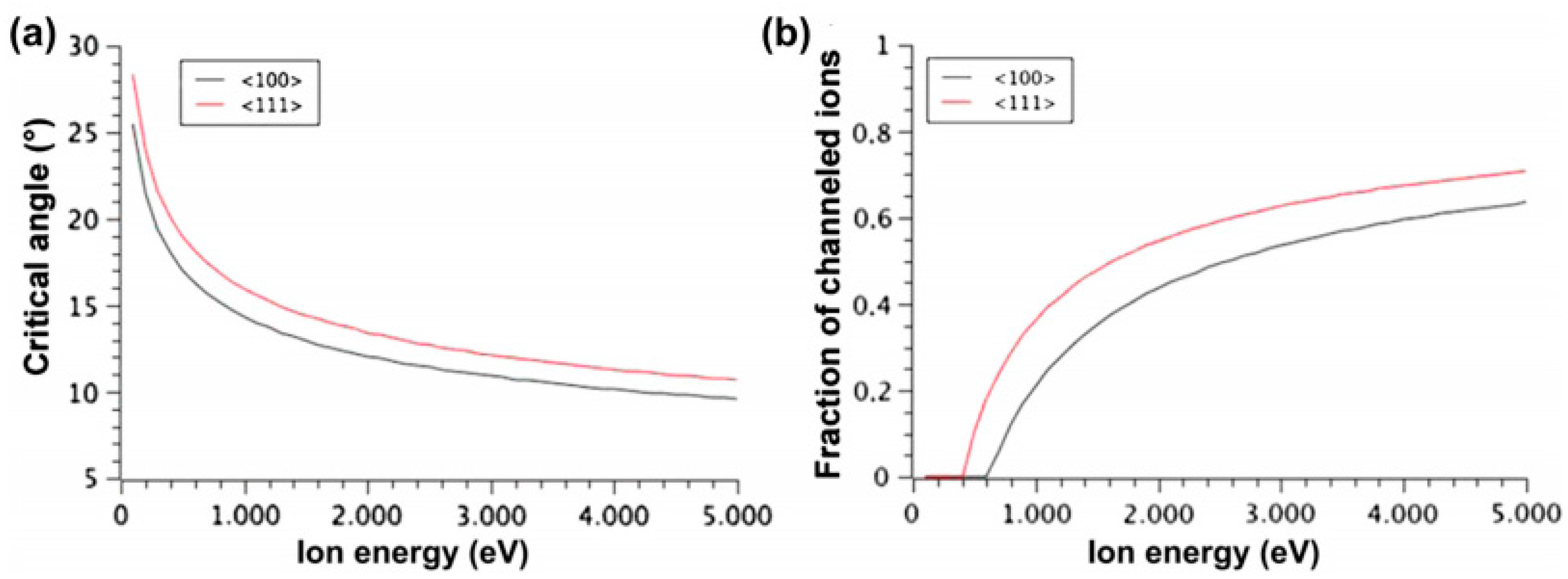
For a particular crystalline axis, only ions incoming within a certain angle can penetrate the channeling rows. This angle is called the critical angle. If the ion velocity is reduced, channeling also does not occur any more below the so-called critical ion energy. Figure 7a shows the critical angle for nitrogen ions into diamond, for (100) and (111) surface orientations. It can be seen that the critical angle becomes very large at low energy. Therefore, a large fraction of channeled ions is expected at these energies, even for high misalignments between the ion beam and the target. For even lower kinetic ion energy, channeling does not occur any more. Thus, a critical angle does not give suitable results [38]. Figure 7b shows the expected fraction of channeled ions in the case of nitrogen in (100) and (111) diamond. It was found that the critical ion energies for channeling are 700 and 400 eV, respectively.
6.3. Other Factors
Several other factors need to be addressed during nitrogen ion implantation on diamond. Diamond is a very wide bandgap (5.5 eV) material with very high resistivity (1016 ohm-cm) [39]. This brings the complicacy during the implantation process. The surface can be charged up during the ion implantation of samples with very high resistivity. In this process, the accumulation of charges may lead to build-up of a very high potential. This charge build-up process can be very detrimental, especially in the case of low-energy ions [40]. Because of the Lorentz force the low-energy ions with low velocity can easily be deviated from their original trajectory. As a result, there occurs a loss in spatial resolution and the implantation yield becomes disoriented. This possible loss of resolution can be avoided (1) by depositing a thin conductive layer on the target diamond sample before implantation; (2) by exposing the sample to an electron shower; or (3) by terminating the diamond surface with hydrogen (to enhance the surface conductivity).
Another factor that needs to be considered is the implantation of molecules or clusters. Molecules immediately dissociate while hitting the diamond target surface and the energy of each atom is given by the mass ratio of the accelerated molecule. For N2 molecules, it is simply half of the implantation energy, and the implantation depth is comparable to monomer ion implantation. However, it is known that cluster implantation reduces the channeling tail but increases the damage. Hence, more and more damage will be accumulated if the diamond is implanted with energetic N2 molecules instead of N ions.
7. Implant Damage and Damage Annealing
During the implantation of N ions in the diamond lattice different kinds of damage are produced as the byproduct, and the creation of this damage in the process is unavoidable. Damage creation depends on several factors such as:
- (1)
- Type of the implant species (heavy ion produces more damage)
- (2)
- Energy of the incident ions (more energy, more ion struggling)
- (3)
- Fluence size (at a fluence size of ~1014 cm−2 or above, extended damage sets in)
- (4)
- Implantation current (high current causes for the overlapping collision cascades)
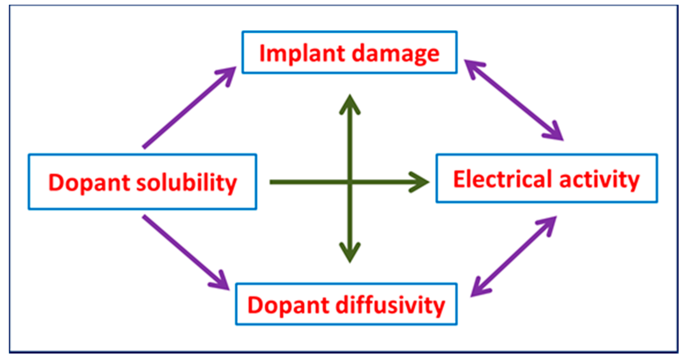
In this study, the type of the implant species is fixed, however, the other factors should be analyzed carefully before any experimental endeavor. Incident energy-related damage formation is covered in Section 6.1. Usually during the production of NV centers in diamond, low fluence size (less than ~1014 cm−2) is used [41]. During the low fluence ion implantation the predominant damage type is point defects, i.e., vacancies, interstitials, or clusters of point defects. High dose rate produces extended defects also known as end-of-range defects. A highly detrimental phenomena known as precipitation of the dopants can occur if the dopant concentration reaches the retrograde solid solubility limit [42]. Annealing temperature must be high enough so that the atoms can move in the lattice, although atoms do not require moving large distances. Theoretically, N atoms can find a lattice site within an atomic distance, which is very short in the case of the diamond lattice. In practice, this phenomenon is quite different, because the defects created by implantation enhance the diffusion process. Usually, the annealing treatment is done by keeping the ion implanted samples in a vacuum furnace at a temperature between 800 °C and 1000 °C. Schwartz et al. studied the effect of low-energy electrons on formation of NV centers in low-energy nitrogen ion implantation on single-crystal diamonds [24]. The implanted single crystal diamond was exposed to the low-energy source, which led to the formation of NV centers without any thermal annealing. However, the overall efficiency during this process was low. On the other hand, a dramatic improvement in the efficiency, as high as 1.8 times compared to the thermal annealing alone, was observed when the implanted single crystal diamond was annealed at 8000 °C. The formation of NV-centers by non-thermal reconstruction of nitrogen-vacancy complexes induced by electronic excitations points to an alternative mechanism for NV-center formation versus trapping of a vacancy by a substitutional nitrogen atom. Activation of most of the nitrogen atoms in the diamond lattice is essential, which is attained by the occupation of the N atoms in the substitutional sites. When the dose size is too high (close to or above the retrograde solid solubility limit) the N atoms occupy the interstitial sites. Figure 8 represents the schematic of the interplay model between the damage and doping in the process of the implantation of N ions in diamond lattice.
8. Problems with Ion Irradiation on Diamond
Although ion implantation is frequently used in the silicon industry to introduce dopants or impurities, and subsequent annealing at few hundred degrees Celsius temperature is good enough to heal a significant portion of damages introduced by the implantation process, the scenario is not the same in case of diamond industry [43]. A number of factors come into the picture, which make the diamond treatment with ion irradiation very complicated.
- (1)
- There exists a critical dose size above which the implantation damage may form complex amorphous or graphitic regions either spontaneously at the time of irradiation or after annealing. The formation of graphitic entities was observed at low ion dose size, as low as 1014 cm−2, during the implantation of 15 N ions at 100 keV energy [25].
- (2)
- High temperature and sometimes high pressure is required to allow the substitutional species/atoms to migrate, which is not an easy process.
- (3)
- At the time of annealing much residual radiation damage or complexes may form, which tend to compensate the implanted dopants.
- (4)
- As the bond lengths in diamond are short, a large concentration of substitutional N atoms create a substantial amount of strain. For this reason, careful measurements/calculations of ion dose, energy, duration of implantation, etc. have to be performed before starting the process.
In practice, the abovementioned problems could be compensated by proper initiatives to generate NV centers. The implanted species lead to deep energy levels in the energy band gap. Hence the implanted diamond can be photo-excited to release holes into the valence band. Implantation of diamond by N ions is less problematic because the damage produced by the irradiation can be exploited to create the NV centers.
9. Discussion
The production of artificial NV centers is feasible using ion implantation. Implantation parameters such as the dose size, ion energy, annealing temperature, etc. all play important roles in determining the final yield of the NV color center-based diamond and the quality of the photonic/electromagnetic signals from the device is also dependent on those parameters. Therefore, selecting such parameters during the fabrication process is very crucial. We can discuss the problems and possible solutions related to good quality NV center-based efficient device fabrication using ion irradiation as follows. Firstly, it is obvious that the energetic N ion implantation process generates lots of vacancy defects in the diamond lattice. One single N ion accelerated with 15 keV energy can produce 70 vacancies, which was verified by the SRIM simulation program by Zeigler et al. [44]. Secondly, most of the N ions in the diamond lattice do not fully yield NV centers. Pezzagna et al. observed that only about 2% of the total N atoms embedded in the diamond lattice after the ion implantation process can form NV centers, whereas the remaining 98% N atoms reside in the diamond lattice to form other defects or remain as an impurity [11]. Decreasing the defect density around the NV centers in the diamond lattice is very crucial in order to improve the quality of optical or photonic yield from the NV centers [45]. To address the above-mentioned issues, based upon the extensive study conducted in this article, here we propose some important ideas which can be utilized during the nitrogen ion implantation in the diamond. Firstly, there is dose size: we can decrease the implanting dose size to create less NV centers, even a single NV center. This is because from quantum computing point of view only six single NV centers separated by some certain distances are necessary to utilize the power of qubit logic. Secondly, we can use an optimum energetic range: by tuning the implanting voltage, one can identify a suitable energy range for the incident N ions at a given dose size. Pezzagna et al. utilized a large range of energies, between 1.5 keV and 18 MeV, in order to give a complete picture of how the yield of NV creation depends on the ion energy [11]. This study suggests that the efficiency of NV defects production strongly depends on the ion implantation energy. In this study a high yield efficiency of 45% was achieved using 18 MeV energetic ions, whereas for energies lower than 5 keV the same was below 1%. It is a common practice to use high voltage for improving the yield efficiency, whereas this process causes the production of a greater number of vacancies and larger straggling due to the high energy ion impact with the lighter C atoms in the diamond matrix (discussed in Section 6.1). Therefore, one can play with the dose size and incident ion energy and tune both of them to find suit spots by some small amounts of tread-off. Hence, these first two conditions could be satisfied to minimize the ratio between unwanted defects and the NV centers. Thirdly, we can use annealing at high temperature: annealing conditions can impact the NV yield efficiency and reduce the overall crystal damage. Naydenov et al. developed a technique of high temperature annealing for improving the yield efficiency as well as the properties of the ion implanted NV centers [46]. Song et al. used inherent vacancies and nitrogen substitutions in nano-diamonds to generate NV centers and the concentration of NV centers increased dramatically after employing the high temperature post annealing treatment [47]. In this study the increase in yield by high temperature thermal annealing process was observed to be as high as eight times. The higher the annealing temperature, the lower the damage related defects. However, selecting a very high temperature will increase the thermal budget. Up to a temperature of 16,000 °C both of the NV(0) and NV(−) photonic centers are quite stable. Therefore, we propose an annealing temperature just above 1000 °C to reduce the defect density more efficiently without affecting the number of NV centers.
Overall from the study conducted here we can infer that the post-irradiation annealing not only contributes significantly to the NV center production but also, by creating divacancies, prevents the formation of negatively charged NV defects. A negatively charged NV(−) center is desirable because most of the diamond applications depend on the presence of this defect. Of course, the annealing is unavoidable to mobilize the vacancies, but a temperature should be chosen in the range where the V2 also becomes mobile, while NV yet does not. Much of the literature shows that V2 starts to anneal out from 800 °C, where NV is not yet mobile [48,49]. As a result, the annealing temperature was selected to be around 1000 °C, which is shown in Figure 4. The annihilation of the divacancies may occur by out-diffusion, via recombination at interstitial clusters, or by the formation of vacancy aggregates, which are also electrically active [50,51]. The displacement energy for permanent lattice damage can considered to be ~50 eV, which is in close agreement with the experimental values suggested by Clarke and Mitchell [52,53]. This value is also in accord with the value (55 eV) for the displacement energy in diamond matrix proposed by Prins et al. [54]. However, studies shown that the vacancy aggregates are acceptor defects with a charge transition level at about Ev + 3.5 eV [55]. This is well above the (0/–) level of NV, so they can donate electrons to turn NV(0) into NV(−). Thus, elimination of V2 can stabilize the charge state of NV(−). The annihilation of V2 is important even when the [NV(−)]/[NV(0)] > 1 condition is achieved after the completion of irradiation and annealing. This is because V2 may become negatively charged when [NV(−)]/[NV(0)] > 1. This can compromise the photo-stability of NV(−). Therefore, getting rid of this effect annihilation of V2 is very crucial. Hence, the high-temperature post-annealing treatments could help stabilize the charge state of NV(−) color centers. In a nutshell, the need of careful characterization of irradiated and annealed diamond samples, particularly focusing on divacancy (V2) or larger vacancy aggregates is required.
From the growth point of view, the depth of an ion implantation and the quality of the final yield depends on the ion species, on its kinetic energy, and on the quality of the target diamond. Moreover, in the case of implantation of molecules or clusters of N the implantation depth is affected, and it has to be taken into account. Additionally, during the ion irradiation the low kinetic energy single-ion beam implantation enables embedding atoms within tens of nanometers, up to 25 nm in case of diamond as shown in Figure 4, in all three dimensions. At present ion implantation is the only reliable technique to produce an array of NV centers with the suitable precision as needed to fabricate a quantum array. However, the requirements and pitfalls are large and therefore care must be taken regarding the surface roughness, channeling effect, or charging up of the surface. Besides technical limitations, the main intrinsic limitation factor is ion beam straggling. Ion beam straggling depends on the ion species and the target atoms and increases strongly with the ion energy, for example, a kinetic ion energy of ~30 keV, and limits the lateral resolution.
Deterministic implantation of N ions to create NV centers in diamond is essential for the quantum technologies. Implanting an exact number of N ions can be realized in two different ways, i.e., (1) by employing a detection system to count the number of ion impacts onto the diamond matrix; or (2) by utilizing a precise ion source which can supply a predetermined number of N ions. The first approach is only possible when the ion energy is 20 keV or higher [56]. Nonetheless, this technique is hard to implement for diamond. In the second approach, an ion trap is utilized to shoot a single ion out to the diamond matrix, which helps to induce a fully deterministic implantation [57]. Utilizing this approach enables us to achieve a very small lateral resolution, as low as 0.1 nm, however implanting a single atom at a time is very time consuming [58]. Additionally, successful implantation of an N ion into the diamond matrix does not necessarily ensure the production of a NV center. All of these limitations related to deterministic ion implantation were taken into account and a novel method for deterministically implanting single ions with sub-nanometer resolution was proposed by Meijer et al. [57]. In this method a linear Paul trap was utilized as an ion source to deliver 2 MeV energetic N+ ions, coupled with sophisticated laser cooling techniques to attain the sub-nanometer resolution and the deterministic control of the number of implanted atoms.
10. Conclusions
In summary, we have broadly covered the formation steps for high quality NV centers by ion implantation process in highly pure crystalline diamond thin films. Special attention was paid to repairing the crystal implantation-related defects, creating the N–V bonds and stabilizing different charge states associated with the NV centers during the production of artificial NV photonic centers using nitrogen ion implantation in diamond. Unfortunately, the creation yield of NV centers is small for low ion energies (a few percent or less). Possible solutions to increase this yield are a post-irradiation and annealing process, a subsequent overgrowth to bury the shallow NV centers, or a surface treatment to find a suitable termination of the surface. Besides the production of the NV defect, the charge state of the center has to be controlled. Passive charge state manipulation is possible either by using an appropriate surface termination or by bringing dopant atoms in the vicinity of the NV centers (by implantation or during the growth of the diamond layer). The production of NV centers in diamond for qubits/quantum communication tasks by ion implantation technique is a very complicated procedure, however, to date it is the only key feature for the production of such centers in diamond quantum devices. More attention should be paid to improving the controllability and scalability for implanting high quality NV centers in crystalline diamond. This will soon enable the NV center-based device fabrication to process information in accordance to the principles of quantum mechanics, which will lead the scientific community to a new technological revolution for humankind.
Acknowledgement
The authors would like to acknowledge Kartik Ghosh and Mahmud Reaz for their useful feedbacks.
Author Contributions
Ariful Haque designed the study, interpreted the idea of the article, conducted analysis on the topic, and designed and wrote the manuscript. Other contributions include special conceptualization of the entire review work, as well as its realization and documentation. Sharaf Sumaiya provided theoretical guidance, contributed to manuscript formation and development of the work. Additionally, she assisted in evaluating and editing the manuscript. All authors gave final approval and agreed to be accountable for all aspects of the work.
Conflicts of Interest
The authors declare no conflict of interest.
References
- Bennett, C.H.; DiVincenzo, D.P. Quantum information and computation. Nature 2000, 404, 247–255. [Google Scholar] [CrossRef] [PubMed]
- Steffen, L.; Salathe, Y.; Oppliger, M.; Kurpiers, P.; Baur, M.; Lang, C.; Eichler, C.; Puebla-Hellmann, G.; Fedorov, A.; Wallraff, A. Deterministic quantum teleportation with feed-forward in a solid state system. Nature 2013, 500, 319–322. [Google Scholar] [CrossRef] [PubMed]
- Griffiths, R.B. Nature and location of quantum information. Phys. Rev. A 2002, 66, 012311. [Google Scholar] [CrossRef]
- Dräbenstedt, A.; Fleury, L.; Tietz, C.; Jelezko, F.; Kilin, S.; Nizovtzev, A.; Wrachtrup, J. Low-temperature microscopy and spectroscopy on single defect centers in diamond. Phys. Rev. B 1999, 60, 11503. [Google Scholar] [CrossRef]
- Hanson, R.; Awschalom, D.D. Coherent manipulation of single spins in semiconductors. Nature 2008, 453, 1043–1049. [Google Scholar] [CrossRef] [PubMed]
- Pan, X.Y.; Liu, G.Q.; Yang, L.L.; Fan, H. Solid-state optimal phase-covariant quantum cloning machine. Appl. Phys. Lett. 2011, 99, 051113. [Google Scholar] [CrossRef]
- Balasubramanian, G.; Chan, I.Y.; Kolesov, R.; Al-Hmoud, M.; Tisler, J.; Shin, C.; Kim, C.; Wojcik, A.; Hemmer, P.R.; Krueger, A.; et al. Nanoscale imaging magnetometry with diamond spins under ambient conditions. Nature 2008, 455, 648–651. [Google Scholar] [CrossRef] [PubMed]
- Babinec, T.M.; Hausmann, B.J.; Khan, M.; Zhang, Y.; Maze, J.R.; Hemmer, P.R.; Lončar, M. A diamond nanowire single-photon source. Nat. Nanotechnol. 2010, 5, 195–199. [Google Scholar] [CrossRef] [PubMed]
- Bhaumik, A.; Haque, A.; Karnati, P.; Taufique, M.F.N.; Patel, R.; Ghosh, K. Copper oxide based nanostructures for improved solar cell efficiency. Thin Solid Films 2014, 572, 126–133. [Google Scholar] [CrossRef]
- DiVincenzo, D.P. The physical implementation of quantum computation. arXiv, 2000; arXiv:preprint quant-ph/0002077. [Google Scholar]
- Pezzagna, S.; Naydenov, B.; Jelezko, F.; Wrachtrup, J.; Meijer, J. Creation efficiency of nitrogen-vacancy centres in diamond. New J. Phys. 2010, 12, 065017. [Google Scholar] [CrossRef]
- Dréau, A.; Spinicelli, P.; Maze, J.R.; Roch, J.F.; Jacques, V. Single-shot readout of multiple nuclear spin qubits in diamond under ambient conditions. Phys. Rev. Lett. 2013, 110, 060502. [Google Scholar] [CrossRef] [PubMed]
- Maertz, B.J.; Wijnheijmer, A.P.; Fuchs, G.D.; Nowakowski, M.E.; Awschalom, D.D. Vector magnetic field microscopy using nitrogen vacancy centers in diamond. Appl. Phys. Lett. 2010, 96, 092504. [Google Scholar] [CrossRef]
- Jelezko, F.; Wrachtrup, J. Single defect centres in diamond: A review. Phys. Status Solidi A 2006, 203, 3207–3225. [Google Scholar] [CrossRef]
- Zaitsev, A.M. Optical Properties of Diamond: A Data Handbook; Springer Science & Business Media: Berlin, Germany, 2013. [Google Scholar]
- Childress, L.; Hanson, R. Diamond NV centers for quantum computing and quantum networks. MRS Bull. 2013, 38, 134–138. [Google Scholar] [CrossRef]
- Tamarat, P.; Manson, N.B.; Harrison, J.P.; McMurtrie, R.L.; Nizovtsev, A.; Santori, C.; Beausoleil, R.G.; Neumann, P.; Gaebel, T.; Jelezko, F.; et al. Spin-flip and spin-conserving optical transitions of the nitrogen-vacancy centre in diamond. New J. Phys. 2008, 10, 045004. [Google Scholar] [CrossRef]
- Santori, C.; Tamarat, P.; Neumann, P.; Wrachtrup, J.; Fattal, D.; Beausoleil, R.G.; Rabeau, J.; Olivero, P.; Greentree, A.D.; Prawer, S.; et al. Coherent population trapping of single spins in diamond under optical excitation. Phys. Rev. Lett. 2006, 97, 247401. [Google Scholar] [CrossRef] [PubMed]
- Tamarat, P.; Gaebel, T.; Rabeau, J.R.; Khan, M.; Greentree, A.D.; Wilson, H.; Hollenberg, L.C.L.; Prawer, S.; Hemmer, P.; Jelezko, F.; et al. Stark shift control of single optical centers in diamond. Phys. Rev. Lett. 2006, 97, 083002. [Google Scholar] [CrossRef] [PubMed]
- Hanson, R.; Gywat, O.; Awschalom, D.D. Room-temperature manipulation and decoherence of a single spin in diamond. Phys. Rev. B 2006, 74, 161203. [Google Scholar] [CrossRef]
- Childress, L.; Dutt, M.G.; Taylor, J.M.; Zibrov, A.S.; Jelezko, F.; Wrachtrup, J.; Hemmer, P.R.; Lukin, M.D. Coherent dynamics of coupled electron and nuclear spin qubits in diamond. Science 2006, 314, 281–285. [Google Scholar] [CrossRef] [PubMed]
- Jelezko, F.; Gaebel, T.; Popa, I.; Gruber, A.; Wrachtrup, J. Observation of coherent oscillations in a single electron spin. Phys. Rev. Lett. 2004, 92, 076401. [Google Scholar] [CrossRef] [PubMed]
- Lesik, M. Engineering of NV Color Centers in Diamond for Their Applications in Quantum Information and Magnetometry. Ph.D. Thesis, Ecole Normale Supérieure, Cachan, Paris, France, 2015. [Google Scholar]
- Schwartz, J.; Aloni, S.; Ogletree, D.F.; Schenke, T. Effects of low-energy electron irradiation on formation of nitrogen–vacancy centers in single-crystal diamond. New J. Phys. 2012, 14, 043024. [Google Scholar] [CrossRef]
- Talapatra, S.; Cheng, J.-Y.; Chakrapani, N.; Trasobares, S.; Cao, A.; Vajtai, R.; Huang, M.B.; Ajayan, P.M. Ion irradiation induced structural modifications in diamond nanoparticles. Nanotechnology 2006, 17, 305–309. [Google Scholar] [CrossRef]
- Evans, T.; Qi, Z. The kinetics of the aggregation of nitrogen atoms in diamond. Proc. R. Soc. Lond. A Math. Phys. Eng. Sci. 1982, 381, 159–178. [Google Scholar] [CrossRef]
- Mainwood, A. Nitrogen and nitrogen-vacancy complexes and their formation in diamond. Phys. Rev. B 1994, 49, 7934. [Google Scholar] [CrossRef]
- Lombardi, E.B.; Mainwood, A.; Osuch, K.; Reynhardt, E.C. Computational models of the single substitutional nitrogen atom in diamond. J. Phys. Condens. Matter 2003, 15, 3135–3149. [Google Scholar] [CrossRef]
- Davies, G.; Lawson, S.C.; Collins, A.T.; Mainwood, A.; Sharp, S.J. Vacancy-related centers in diamond. Phys. Rev. B 1992, 46, 13157. [Google Scholar] [CrossRef]
- Pinto, H.; Jones, R.; Palmer, D.W.; Goss, J.P.; Briddon, P.R.; Öberg, S. On the diffusion of NV defects in diamond. Phys. Status Solidi A 2012, 209, 1765–1768. [Google Scholar] [CrossRef]
- Deák, P.; Aradi, B.; Kaviani, M.; Frauenheim, T.; Gali, A. Formation of NV centers in diamond: A theoretical study based on calculated transitions and migration of nitrogen and vacancy related defects. Phys. Rev. B 2014, 89, 075203. [Google Scholar] [CrossRef]
- Haque, A.; Rahman, M.A.; Ahsan, Q. Building integrated photovoltaic system: Cost effectiveness. In Proceedings of the 2012 IEEE 7th International Conference on Electrical & Computer Engineering (ICECE), Dhaka, Bangladesh, 20–22 December 2012; pp. 904–907. [Google Scholar]
- Grotz, B.; Hauf, M.V.; Dankerl, M.; Naydenov, B.; Pezzagna, S.; Meijer, J.; Jelezko, F.; Wrachtrup, J.; Stutzmann, M.; Reinhard, F.; et al. Charge state manipulation of qubits in diamond. Nat. Commun. 2012, 3, 729. [Google Scholar] [CrossRef] [PubMed]
- Goss, J.P.; Briddon, P.R.; Rayson, M.J.; Sque, S.J.; Jones, R. Vacancy-impurity complexes and limitations for implantation doping of diamond. Phys. Rev. B 2005, 72, 035214. [Google Scholar] [CrossRef]
- Khmelnitsky, R.A.; Dravin, V.A.; Tal, A.A.; Zavedeev, E.V.; Khomich, A.A.; Khomich, A.V.; Alekseev, A.A.; Terentiev, S.A. Damage accumulation in diamond during ion implantation. J. Mater. Res. 2015, 30, 1583–1592. [Google Scholar] [CrossRef]
- Yamamoto, T.; Umeda, T.; Watanabe, K.; Onoda, S.; Markham, M.L.; Twitchen, D.J.; Naydenov, B.; McGuinness, L.P.; Teraji, T.; Koizumi, S.; et al. Extending spin coherence times of diamond qubits by high-temperature annealing. Phys. Rev. B 2013, 88, 075206. [Google Scholar] [CrossRef]
- Pezzagna, S.; Meijer, J. Single-Ion Implantation in Diamond with a High Lateral Resolution-3.13: A Key Technology for the Fabrication of Quantum Devices. In Comprehensive Hard Materials; Sarin, V.K., Ed.; Elsevier: Oxford, UK, 2014; pp. 321–336. [Google Scholar]
- Hobler, G. Monte Carlo simulation of two-dimensional implanted dopant distributions at mask edges. Nucl. Instrum. Methods Phys. Res. Sect. B Beam Interact. Mater. Atoms 1995, 96, 155–162. [Google Scholar] [CrossRef]
- Saslow, W.; Bergstresser, T.K.; Cohen, M.L. Band Structure and Optical Properties of Diamond. Phys. Rev. Lett. 1966, 16, 354, Erratum 1968, 21, 715. [Google Scholar] [CrossRef]
- Arifin, M.S.; Khan, M.M.S.; Haque, A. Improvement of load-margin and bus voltage of Bangladesh power system with the penetration of PV based generation. In Proceedings of the 2013 IEEE International Conference on Informatics, Electronics & Vision (ICIEV), Dhaka, Bangladesh, 17–18 May 2013; pp. 1–5. [Google Scholar]
- Toyli, D.M.; Weis, C.D.; Fuchs, G.D.; Schenkel, T.; Awschalom, D.D. Chip-scale nanofabrication of single spins and spin arrays in diamond. Nano Lett. 2010, 10, 3168–3172. [Google Scholar] [CrossRef] [PubMed]
- Jones, K.S.; Allen, E.L.; Robinson, H.G.; Stevenson, D.A.; Deal, M.D.; Plummer, J.D. Extended defects of ion-implanted GaAs. J. Appl. Phys. 1991, 70, 6790–6795. [Google Scholar] [CrossRef]
- Saguy, C.; Reznik, A.; Baskin, E.; Remes, Z.; Kalish, R. Defect-dopant interaction in n-and p-type diamond and its influence on electrical properties. Diam. Relat. Mater. 2004, 13, 722–726. [Google Scholar] [CrossRef]
- Zeigler, J.F.; Biersack, J.P.; Littmark, U. The Stopping and Range of Ions in Matter; SRIM-2008; Springer: Boston, MA, USA, 1985. [Google Scholar]
- Cui, J.-M.; Chen, X.-D.; Fan, L.-L.; Gong, Z.-J.; Zou, C.-W.; Sun, F.-W.; Han, Z.-F.; Guo, G.-C. Generation of nitrogen-vacancy centers in diamond with ion implantation. Chin. Phys. Lett. 2012, 29, 036103. [Google Scholar] [CrossRef]
- Naydenov, B.; Reinhard, F.; Lämmle, A.; Rafi Kalish, V.R.; D’Haenens-Johansson, U.F.S.; Newton, M.; Jelezko, F.; Wrachtrup, J. Increasing the coherence time of single electron spins in diamond by high temperature annealing. Appl. Phys. Lett. 2010, 97, 242511. [Google Scholar] [CrossRef]
- Song, X.; Wang, G.; Liu, X.; Feng, F.; Wang, J.; Lou, L.; Zhu, W. Generation of nitrogen-vacancy color center in nanodiamonds by high temperature annealing. Appl. Phys. Lett. 2013, 102, 133109. [Google Scholar] [CrossRef]
- Clark, C.D.; Ditchburn, R.W.; Dyer, H.B. The absorption spectra of irradiated diamonds after heat treatment. Proc. R. Soc. Lond. A Math. Phys. Eng. Sci. 1956, 237, 75–89. [Google Scholar] [CrossRef]
- Iakoubovskii, K.; Stesmans, A. Chemical vapour deposition diamond studied by optical and electron spin resonance techniques. J. Phys. Condens. Matter. 2002, 14, R467–R499. [Google Scholar] [CrossRef]
- Iakoubovskii, K.; Stesmans, A. Dominant paramagnetic centers in 17 O-implanted diamond. Phys. Rev. B 2002, 66, 045406. [Google Scholar] [CrossRef]
- Habib, S.; Haque, A.; Rahman, J. Production of MHD power from municipal waste & Algal biodiesel. In Proceedings of the 2012 IEEE International Conference on Informatics, Electronics & Vision (ICIEV), Dhaka, Bangladesh, 18–19 May 2012; pp. 1097–1100. [Google Scholar]
- Wu, W.; Fahy, S. Molecular-dynamics study of single-atom radiation-damage in diamond. Phys. Rev. B 1994, 49, 3030. [Google Scholar] [CrossRef]
- Clark, C.D.; Mitchell, E.W.J. Radiation sects in Semiconductors. In IOP Conference Proceedings No. 31; Urli, N.B., Corbett, J.W., Eds.; Institute of Physics and Physical Society: London, UK, 1977; p. 45. [Google Scholar]
- Prins, J.F.; Derry, T.E.; Sellschop, J.P.F. Volume expansion of diamond during ion implantation. Phys. Rev. B 1986, 34, 8870. [Google Scholar] [CrossRef]
- Khan, R.U.A.; Cann, B.L.; Martineau, P.M.; Samartseva, J.; Freeth, J.J.P.; Sibley, S.J.; Hartland, C.B.; Newton, M.E.; Dhillon, H.K.; Twitchen, D.J. Colour-causing defects and their related optoelectronic transitions in single crystal CVD diamond. J. Phys Condens. Matter 2013, 25, 275801. [Google Scholar] [CrossRef] [PubMed]
- Jamieson, D.N.; Yang, C.; Hopf, T.; Hearne, S.M.; Pakes, C.I.; Prawer, S. Controlled shallow single-ion implantation in silicon using an active substrate for sub-20-keV ions. Appl. Phys. Lett. 2005, 86, 202101. [Google Scholar] [CrossRef]
- Meijer, J.; Vogel, T.; Burchard, B.; Rangelow, I.W.; Bischoff, L.; Wrachtrup, J.; Domhan, M.; Jelezko, F.; Schnitzler, W.; Schulz, S.A. Concept of deterministic single ion doping with sub-nm spatial resolution. Appl. Phys. A Mater. Sci. Proc. 2006, 83, 321–327. [Google Scholar] [CrossRef]
- Schnitzler, W.; Jacob, G.; Fickler, R.; Schmidt-Kaler, F.; Singer, K. Focusing a deterministic single-ion beam. New J. Phys. 2010, 12. [Google Scholar] [CrossRef]
Figure 1.
Schematic of (a) NV(0) center and (b) NV(−) center in a diamond unit cell. NV: nitrogen-vacancy.
Figure 1.
Schematic of (a) NV(0) center and (b) NV(−) center in a diamond unit cell. NV: nitrogen-vacancy.

Figure 2.
(a) Electronic band structure of an ‘atom-like’ NV center showing the ground state and excited state; (b) Normalized photoluminescence spectra of NV(0) (red) and NV(−) (blue) color centers. The red and the blue spectra elucidate the two peaks associated with the zero phonon line at 575 nm (2.156 eV) and 637 nm (1.945 eV). The solid gray circles in the inset denote the available five electrons in the NV(0) center. The additional trapped electron in the NV(−) center is represented by the dashed blue circle. The white, green and blue spheres denote an N atom, a C atom and a single vacancy site in the diamond lattice, respectively. Adapted from [23].
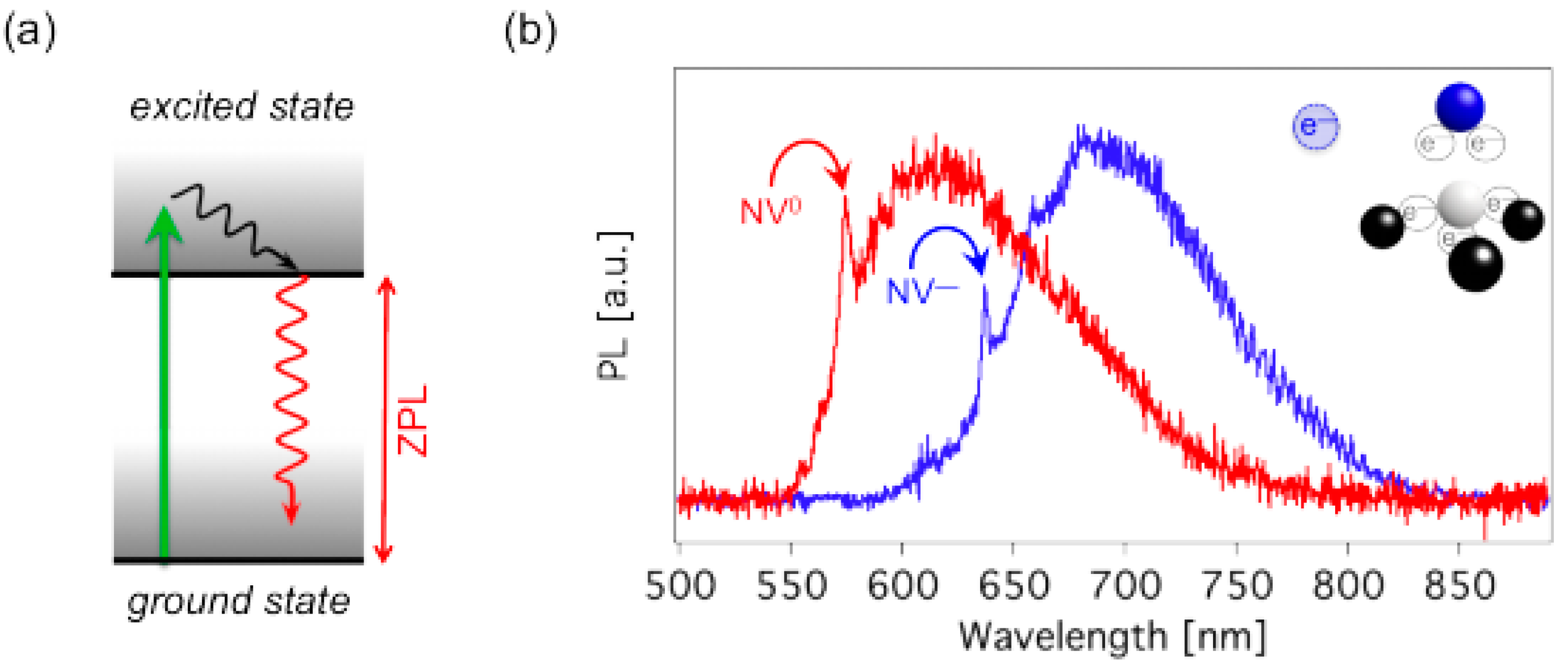
Figure 3.
Defect concentrations over a wide range of initial nitrogen concentration in diamond lattice after performing annealing treatment at 1100 K. (a) shows the concentration of Ns(+), Ns(0), Ns(−), and NV(−) defects and (b) shows the concentration of Ns(+), N2(0), N2V(0), and N2V(−) defects. Ns: substitutional nitrogen. Reprinted with permission from Deák, P.; Aradi, B.; Kaviani, M.; Frauenheim, T.; Gali, A. Formation of NV centers in diamond: A theoretical study based on calculated transitions and migration of nitrogen and vacancy related defects. Phys. Rev. B 2014, 89, 075203. Copyright (2014) by the American Physical Society.

Figure 4.
Schematic of irradiation of diamond by 14N and generation of NV centers.
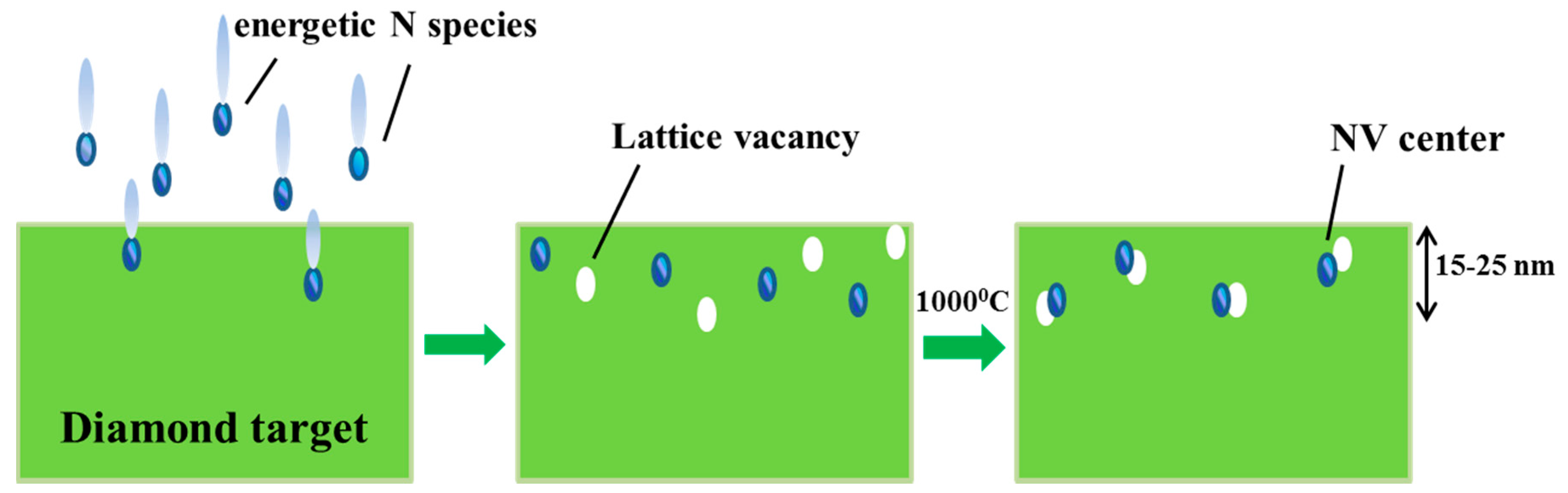
Figure 5.
(a) Stopping and range of ions in matter (SRIM) simulation (trajectories) of nitrogen ions implanted into diamond with kinetic energies of 5 keV and 1 MeV. The need to use low ion energies to ensure low straggling and hence high-resolution implantation is shown; (b) Depth profile of the concentration of 5-keV nitrogen atoms calculated for a dose size of 1 × 1012 cm−2; (c) Depth profile of the concentration of 1-MeV nitrogen atoms calculated for the same dose size. Adapted from [37].
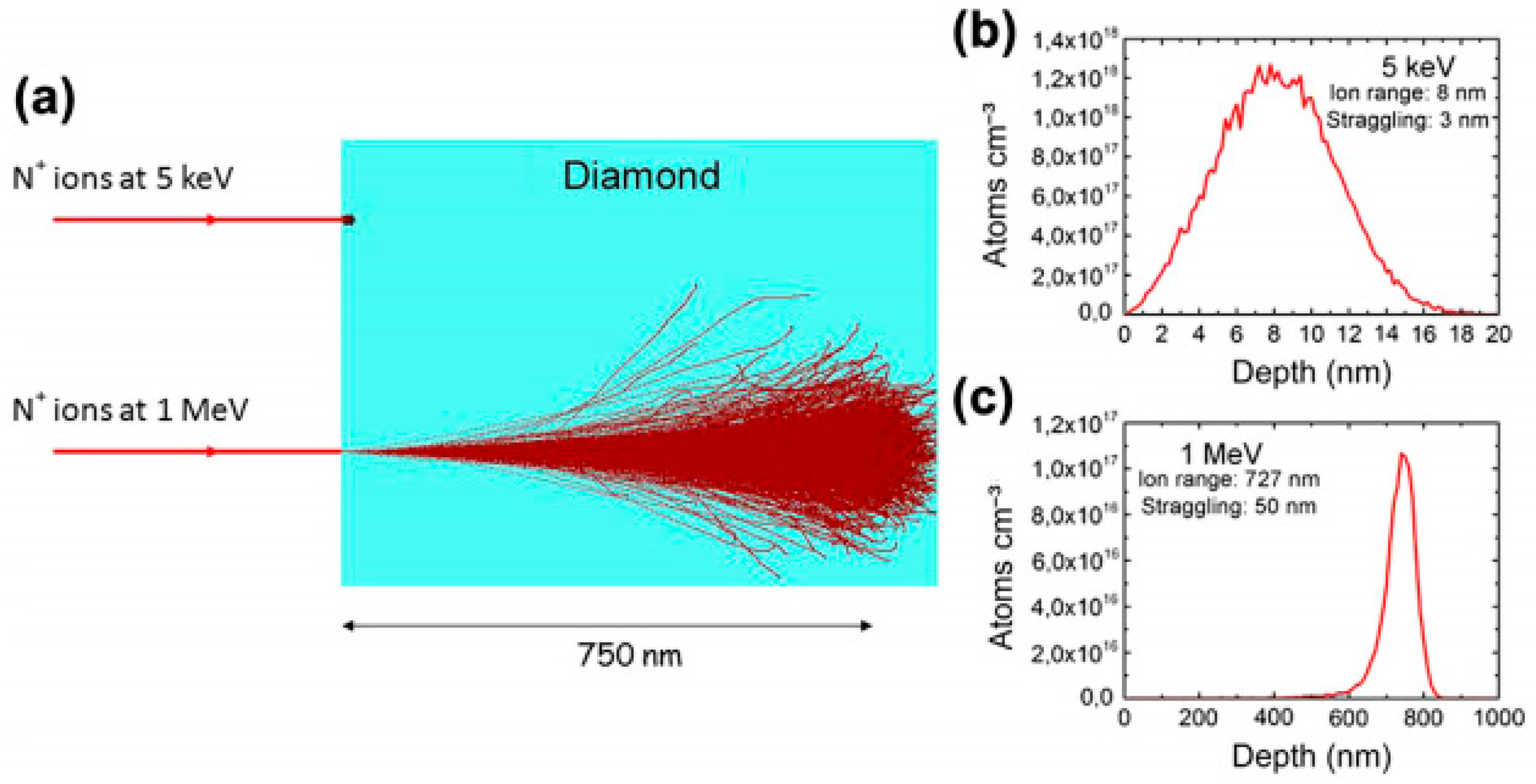
Figure 6.
Results from SRIM software simulation showing the spatial distribution (penetration depth in nm) of the low-energy (5 keV or less) nitrogen ions in the diamond lattice as a function of the kinetic energy of the incident ions. Adapted from [23].
Figure 6.
Results from SRIM software simulation showing the spatial distribution (penetration depth in nm) of the low-energy (5 keV or less) nitrogen ions in the diamond lattice as a function of the kinetic energy of the incident ions. Adapted from [23].
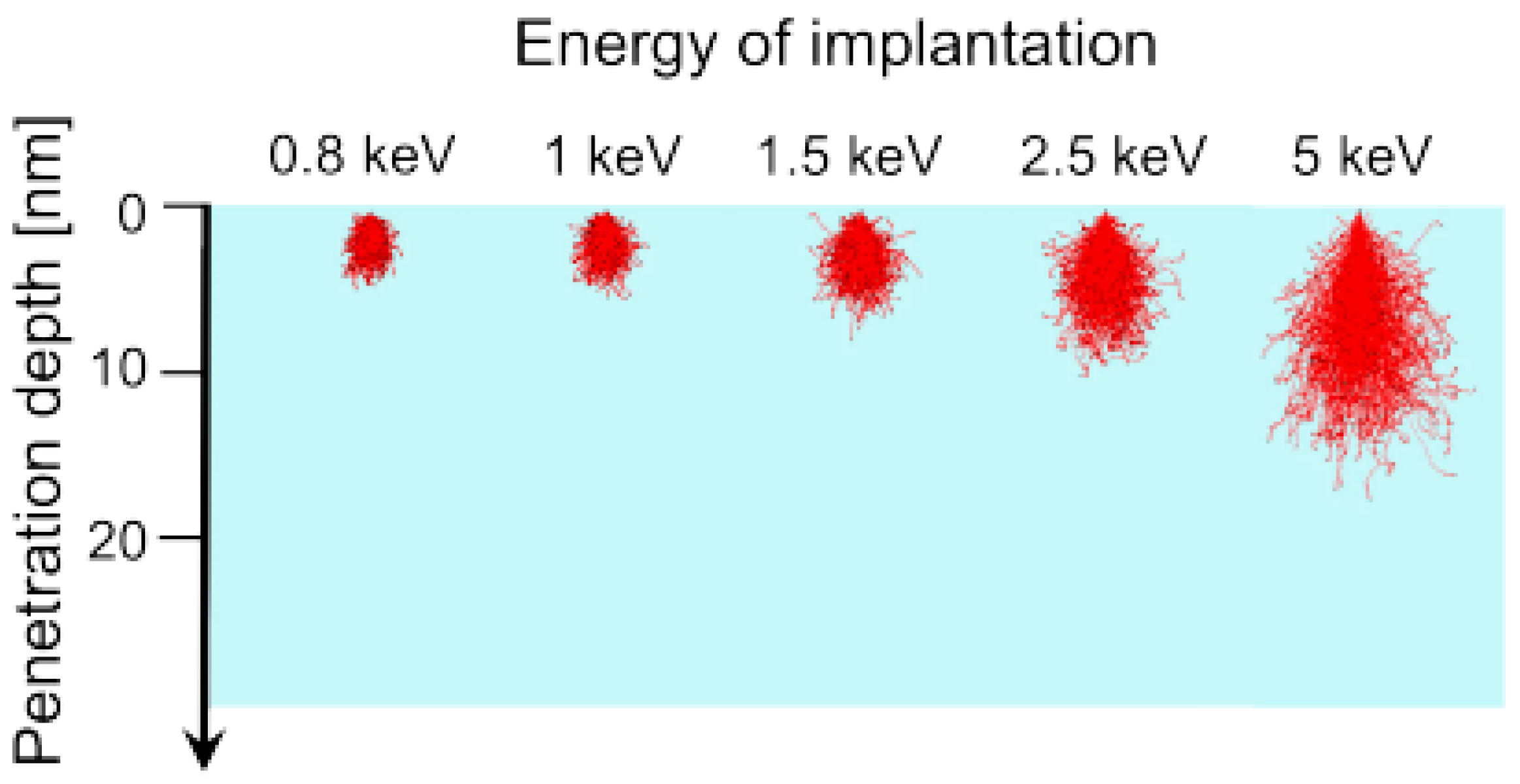
Figure 7.
(a) Critical angle for low-energy nitrogen ions in (100) and (111) diamond; (b) Fraction of channeled ions in (100) and (111) diamond. Adapted from [37].
Figure 7.
(a) Critical angle for low-energy nitrogen ions in (100) and (111) diamond; (b) Fraction of channeled ions in (100) and (111) diamond. Adapted from [37].

Figure 8.
Schematic of the implantation–diffusion interaction model during nitrogen ion implantation and post annealing treatment in diamond.
Figure 8.
Schematic of the implantation–diffusion interaction model during nitrogen ion implantation and post annealing treatment in diamond.

© 2017 by the authors. Licensee MDPI, Basel, Switzerland. This article is an open access article distributed under the terms and conditions of the Creative Commons Attribution (CC BY) license (http://creativecommons.org/licenses/by/4.0/).
Share and Cite
MDPI and ACS Style
Haque, A.; Sumaiya, S. An Overview on the Formation and Processing of Nitrogen-Vacancy Photonic Centers in Diamond by Ion Implantation. J. Manuf. Mater. Process. 2017, 1, 6. https://doi.org/10.3390/jmmp1010006
AMA Style
Haque A, Sumaiya S. An Overview on the Formation and Processing of Nitrogen-Vacancy Photonic Centers in Diamond by Ion Implantation. Journal of Manufacturing and Materials Processing. 2017; 1(1):6. https://doi.org/10.3390/jmmp1010006
Chicago/Turabian StyleHaque, Ariful, and Sharaf Sumaiya. 2017. "An Overview on the Formation and Processing of Nitrogen-Vacancy Photonic Centers in Diamond by Ion Implantation" Journal of Manufacturing and Materials Processing 1, no. 1: 6. https://doi.org/10.3390/jmmp1010006