Article

Structure and Electrical Properties of Carbon-Rich Polymer Derived Silicon Carbonitride (SiCN)

by
Oluwole Daniel Adigun
1,2,3,*,
Emmanuel Ricohermoso III
2,
Ayodele Abeeb Daniyan
1,
Lasisi Ejibunu Umoru
1 and
Emanuel Ionescu
2,4
1
Department of Materials Science and Engineering, Obafemi Awolowo University, Ile Ife 220101, Nigeria
2
Fachbereich Material-Und Geowissenschaften, Technische Universitat Darmstadt, 64287 Darmstadt, Germany
3
Department of Metallurgical and Materials Engineering, Federal University Oye, Oye-Ekiti 370111, Nigeria
4
Fraunhofer IWKS, Department Digitalization of Resources, Brentanostr. 2a, 63755 Alzenau, Germany
*
Author to whom correspondence should be addressed.
Ceramics 2022, 5(4), 690-705; https://doi.org/10.3390/ceramics5040050
Submission received: 25 August 2022 / Revised: 20 September 2022 / Accepted: 27 September 2022 / Published: 3 October 2022
(This article belongs to the Special Issue Ceramics for Decarbonization of the Global Industry)

Abstract

:
This article reports on the structure and electronic properties of carbon-rich polysilazane polymer-derived silicon carbonitride (C/SiCN) corresponding to pyrolysis temperatures between 1100 and 1600 °C in an argon atmosphere. Raman spectroscopy, X-ray diffraction (XRD), energy dispersive X-ray spectroscopy (EDX), Scanning Electron Microscopy (SEM) and Hall measurements were used to support the structural and electronic properties characterization of the prepared C/SiCN nanocomposites. A structural analysis using Raman spectroscopy showed the evolution of sp2 hybridized carbon phase that resulted from the growth in the lateral crystallite size (La), average continuous graphene length including tortuosity (Leq) and inter-defects distance (LD) with an increase in pyrolysis temperature. The prepared C/SiCN monoliths showed a record high room temperature (RT) electrical conductivity of 9.6 S/cm for the sample prepared at 1600 °C. The electronic properties of the nanocomposites determined using Hall measurement revealed an anomalous change in the predominant charge carriers from n-type in the samples pyrolyzed at 1100 °C to predominantly p-type in the samples prepared at 1400 and 1600 °C. According to this outcome, tailor-made carbon-rich SiCN polymer-derived ceramics could be developed to produce n-type and p-type semiconductors for development of the next generation of electronic systems for applications in extreme temperature environments.

1. Introduction

Broad studies on the electrical properties of polymer-derived ceramics (also called PDCs, e.g., SiC, SiCN, SiOCN, SiOC, etc.) and their composites have been on the rise in recent years [1,2]. Motivation for such extensive studies is centered on the tailorability of their structure, easy shaping processes and their functional applications, particularly in the area of semiconductor-based electronic systems such as micro-electromechanical systems (MEMS) and microsensors for applications in high-temperature environments [3,4,5]. These materials have demonstrated features that announce properties already known for conventional silicon-based semiconductors and have equally shown unique properties beyond what was previously achievable. Among these classes of semiconducting ceramic materials, the non-oxide silicon carbonitrides (SiCN), have shown both higher temperature stability in terms of oxidation and creep resistance (≥1600 °C) and wider band gap (at room temperature) over others [6,7,8,9].
While amorphous Si-C-N produced by the pyrolysis of polysilazane at a temperature <1200 °C in inert atmosphere is made up of a single SixCyNz phase and free carbon, the crystalline state pyrolyzed beyond ~1350 °C comprises of SiC, Si3N4 and C nanocomposite phases (C is free carbon; also called sp2 hybridized carbon, turbostratic carbon or graphitic carbon) [10,11,12]. The amorphous phase is associated with very low electrical conductivity (σdc), in the range of 10−9 to 10−2 S/cm, but a vast increase of several orders of magnitude is observed as the material transforms to crystalline state via increase in pyrolysis temperature [13,14]. Over the years, the strong increase in room temperature (RT) conductivity has been attributed to increase in pyrolysis temperature during thermal treatment of the material, which in turn leads to the following: (i) structural transformation of the carbon phase from amorphous carbon to ordered sp2-hybridized carbon (Note that the RT conductivity of sp2 hybridized carbon is 10° to 105 S/cm); (ii) crystallization of β-SiC (Note that only SiC and sp2-hybridized carbon are semiconductors in the composition, Si3N4 is an insulator and does not contribute to conductivity); and (iii) Nitrogen (N) doping of the β-SiC as Si3N4 (in the SiC,/Si3N4/C nanocomposite) decomposes gradually to give off N2 gas at higher temperatures when T > ~1400 °C [9,15]. While these assertions have been proven and corroborated by various characterization techniques such as XANES spectroscopy, XRD, TEM and Raman Spectroscopy, a profound understanding of the electrical conductivity of SiCN PDCs, particularly the charge carrier transport mechanisms, remain incomplete. Seeing the emerging potential of SiCN as semiconductor materials for the next generation of electronics for applications in extreme temperature environments, developing an understanding of the carrier transport mechanism is important in order to study the principle leading to its electrical conductivity as this could aid in their fabrication for various useful electronic purposes.
Evaluation of the electrical conductivity of polysilazane-derived SiCN began in the early 90s with the work of Mocaer but studies on their charge carrier transport are still very rare to come by in the literature [16,17]. One of the ways to determine carrier mobility (μH), carrier type (n-type or p-type), carrier density/concentration (N), conductivity (σdc) and other useful electrical conductivity parameters in a semiconductor is through Hall measurement. The principle and efficiency of Hall measurement technique for the assessment of semiconductivity in shaped crystal articles and thin films have been emphasized [18,19]. Usually, semiconductor materials either possess a majority positive or negative charge carriers signifying p-type or n-type semiconductors, respectively. However, some materials appear to have played out the two charge carrier types as majority carriers at the same time under different conditions. In a recent study aimed at characterizing the electrical properties of SiCN(O) PCDs, Ryu et al. revealed that some samples gave both positive and negative signs of Hall coefficient, but it could not be inferred as to whether the samples were of p–type or n-type semiconductors [16].
Similarly, the question of why a single material possesses both positive and negative Hall coefficient (i.e., both n and p-type majority charge carriers) is still a subject of unresolved debate [20,21]. The compositions, processing conditions, and the nanostructure of the materials could be the intrinsic source of these observations. For instance, after assessing the effect of thermal treatments on the electrical conductivity of SiCN and SiBCN ceramics, Hermann et al. recently reported that addition of boron increased the on-set crystallization temperature of SiCN PDC because boron retarded the atomic mobility, and the Si(B)CN ceramic showed higher RT conductivity than the as-pyrolyzed SiCN ceramics [22]. Besides the use of metal addition to improve electrical properties, conscious formation of sp2 hybridized carbon phases by raising the carbon content can also help increase electrical properties of PDCs. This can be achieved via custom-made precursor synthesis [23], mixing of different commercially available precursors [24] or direct addition of a suitable crosslinker [25,26]. Among these approaches, it is the direct addition of a suitable cross-linker that is the most straightforward and easy. Divinylbenzene (DVB) is a common cross-linking agent used to adjust the resulting chemical and structural composition of PDCs by increasing the carbon content and molecular weight/ceramic yield [27]. The resulting formation of sp2 hybridized carbon phase from the rise in carbon content has been shown to be beneficial to electrical properties [26,28]. The type of the inert atmosphere adopted during thermal treatment has also been identified as a crucial factor that determines electrical conductivity behaviour via carbothermic composition adjustments [9]. In [9], Haluschka et al. investigated the influence of ammonia (NH3) alone and argon (Ar)/ammonia gas mixture atmosphere on thermally induced RT conductivity of SiCN and reported that free carbon content of the materials is reduced due to enhanced methane evolution in the ammonia (NH3) atmosphere, resulting in a progressive replacement of carbon by nitrogen and this led to decrease in RT electrical conductivity by up to 4 orders of magnitude. Consequently, the electrical conductivity of semiconductor engineering ceramics can also be modified through the choice of pyrolysis atmosphere. So far, some applications of electrically conducting carbon rich PDCs where tailoring the chemical composition could influence the properties of the ceramics and make them of functional use have been displayed in batteries or electrocatalysis [29,30,31]. Motivated by the exceptional properties of carbon rich PDCs that have evolved in the recent past and the high temperatures stability of SiCN PDCs, it is believed that a tailor-made chemical composition of carbon rich SiCN could hold prospects for novel discoveries in other application areas such as thermopower or high temperature electronics that requires basically p-type and n-type semiconductors. Moreover, investigation of the ordering of the sp2-hybridized free carbon phase in SiOC/C PDCs via thermal treatment reported by Rosenburg et al. [24] could be replicated in the carbon rich SiCN systems for the extraction of innovative information, and this is where the current study comes in.
Here we present the electrical properties of carbon-rich SiCN (up to ca. 72 at. % carbon) with attention to the observed anomalous shift in the dominant charge carriers from n-type in the amorphous glassy matrix pyrolyzed at 1100 °C to mainly p-type in the crystalline ceramic samples prepared at 1400–1600 °C. Such resulting technical ceramics could be of great interest for the development of semiconductors applied in harsh environments. The amount, size and evolution of the sp2-hybridized free carbon phase with the thermal treatment in an argon atmosphere as well as the charge carrier transport mechanism are characterized using Raman spectroscopy, Energy Dispersive X-ray Spectroscopy, EDX attached to a (High Resolution) Scanning Electron Microscopy –SEM, X-ray diffraction (XRD) and Hall measurements. The produced C/SiCN materials also show RT electrical conductivity (0.148–9.26 S/cm) that are quite higher than previously reported values for monolith samples produced using similar pyrolysis temperatures. Consequently, depending on the processing and the final chemical composition, C-rich SiCN PDCs may be tailored to produce n-type and p-type semiconductors for the development of the next generation of micro-electromechanical systems (MEMS) and other microelectronic devices for applications in extremely high temperature environments.

2. Experimental Procedures

2.1. Synthesis

Commercially available Durazane 1800 (Merck KGaA, Darmstadt, Germany) was used as the primary polysilazane polymer for the fabrication of the carbon-rich SiCN samples with 50 wt% Divinlybenzene, DVB (Sigma-Aldrich, subsidiary of Merck KGaA, Darmstadt, Germany) as a crosslinking agent in the presence of Platinum divinyl-tetramethyl disiloxane complex, ∼Pt 2% in xylene (Sigma-Aldrich, subsidiary of Merck KGaA, Darmstadt, Germany) diluted to 0.1%, as catalyst. The composition was thoroughly stirred with a magnetic stirrer for 6 h at 120 °C for the hydrosilylation reaction which was done using standard Schlenk techniques in an argon atmosphere. All through the synthesis, the composition was appropriately confined under an argon atmosphere and thoroughly degassed at each point in vacuum to eliminate any dissolved impurities -due to the sensitivity of polysilazane towards oxygen and humidity. The composition was cross-linked at 250 °C for 3 h in an argon atmosphere to obtain an infusible preceramic solid which was ground for 2 h in a milling machine (Mixer Mill MM400, Retsch, Germany) to obtain very fine powder of about 40 µm. Approximately 200 mg of the preceramic powder was consolidated in a Ø 10 mm die using a warm press at 250 °C and 18 kN to form a green body. Consequently, the green body was pyrolyzed at 1100 °C and annealed at 1400 °C ≤ T ≤ 1600 °C in an argon atmosphere to obtain C/SiCN nanocomposite monoliths. Additional descriptions of polysilazane monolith fabrication processes are reported in the literature [32,33].

2.2. Characterization

The elemental composition was determined using Energy Dispersive X-ray Spectroscopy, EDX, attached to a (High Resolution) Scanning Electron Microscopy, SEM (Philips XL30 FEG, Phillips, Hillsboro, OR, USA) while the morphology characterization was done using the SEM images. Crystallization of the C/SICN powders was investigated using X-ray diffraction (XRD) in the transmission mode by STOE STAD1 P (STOE & Cie. GmbH, STOE, Darmstadt, Germany) using monochromatic Mo Kα radiation at 0.1°/step with 25 s acquisition time for each step in the 2theta range of 5–45°; consequently, the samples were investigated with a D8 Advance diffractometer (Bruker AXS GmbH, Karlsruhe, Germany) with Cu Kα radiation in a reflection mode. The sp2-hybridized carbon phase was analysed using Raman spectroscopy (HR Raman Spectroscope HR800, Horiba Jobin Yvon GmbH, Bensheim, Germany). The electrical conductivity and Hall measurements were investigated using the Van der Pauw method as described in [34].

3. Results and Discussion

3.1. Investigation of the Carbon Phase

Previous studies have shown that polysilazane-derived amorphous SiCN ceramics pyrolyzed at 900–1100 °C consist of mixed SixCyNz bond and free carbon [35]. At a higher ceramization temperature (above ~1350 °C), however, the microstructure evolves into crystalline nanodomains made up of SiC, Si3N4 and C with the sp2 hybridized carbon phase playing a major role in influencing the functional properties of the SiCN material [35,36,37].
The microstructural evolution of the sp2 hybridized carbon phase in the prepared carbon-rich SiCN samples was investigated using Raman Spectroscopy. The primary signals of the Raman spectra showing the carbon phase are the D and G bands identified at ~1350 cm−1 and ~1582 cm−1, respectively, for the monoliths (see Figure 1a–c), but the secondary signals include prominent overtones and combination bands which are the 2D (or G’), 2D’, T + D and D + G bands in the range of ~2500–3250 cm−1 [38,39]. A D’ band (at ~1500 cm−1) and T (~1200 cm−1) band which relate to amorphous carbon fractions and sp2-sp3 C-C/C=C bonds respectively revealed in the monoliths are other two crucial bands that often stretch from the G and D band shoulders most especially shown in amorphous materials. The D’ and T bands are prominent in the amorphous SiCN monolith samples produced at the pyrolysis temperature of 1100 °C. In the sample annealed at 1600 °C, a signal at ca. 820 cm−1 was identified and assigned to β-SiC. In general, the peak position, width, intensities and overlapping Raman spectra give useful details on the structural evolution, defects and crystallite size of the graphitic carbon phase. The D band is a defect-prompted band that results due to a corresponding disorder (amorphization) from carbon nanostructure while the G band is formed by the internal stretching of highly ordered sp2 hybridized carbon lattice [9,40,41]. At the temperature of 1100 °C, the D and G bands of the samples are seen to overlap which complicates separation of the profiles but at a temperature of ≥1400 °C, overlapping of the D and G bands has been greatly reduced (see Figure 1a–c). Moreover, Lorentzian fitting of the Raman bands was performed in order to extract information about the structural evolution of the carbon phase at elevated temperatures; and the rising intensities of the 2D band noticed in the prepared samples with an increase in temperature from 1100 °C to 1600 °C is an important indicator of the rising crystallinities of the graphitic nanostructure.
The lateral size of sp2 hybridized carbon, La, used to characterize the width of the graphitic crystallite of the samples along the a-axis, was determined using Equation (1) [42,43,44]. Where AD/AG is integrated intensities ratio of the D and G bands and ʎ is the laser line wavelength (514 nm).
L a = ( 2.4   ×   10 10 )   ʎ L 4 ( A D A G ) 1
The consistency of the integrated intensities ratio and its importance in the observation of the quantum Hall effect in graphitic materials for the design and fabrication of target electronic systems have been discussed in various studies [42,43,45]. The dependence of the lateral crystal size, La, of the graphitic nanostructure of the samples on the integrated intensities of the D and G bands, as well as its reliance on the thermal treatment, is presented in Figure 2a. The crystallite size, La, increased as the annealing temperatures used in making the samples increased between 1100 °C and 1600 °C. La reveals the width of a single sp2 hybridized carbon crystal unit and analysis of the Raman spectra shows that during the thermal processing, smaller crystallites grow to form larger size with higher degree of structural orderliness. This increase in crystallite size could be linked to kinetics generated within the materials during the annealing process. At 1600 °C, the crystallite size of the graphitic carbon has grown to ca. 10 nm (from ca. 7.7 nm at 1100 °C, see Figure 2a). Moreover, a recorded increase in La as a result of increased ceramization temperatures conforms with the work of Ricohermoso et al. as well as Rosenburg et al., who both studied the evolution of the sp2-hybridized carbon phase in polymer-derived SiOC ceramics [24,46]. An improvement in the structural stability of a graphitic material in terms of strength and ductility could also be achieved via nucleation of the sp2 carbon crystallite size as discussed in a recent study [47]. In the same vein, Tarhini et al. revealed that a lateral crystallite size, La, greater than 7 nm led to improvements in in-plane electrical conductivity, thermal conductivity and tensile strength [48]. Therefore, an increase in La with temperature increases indicate corresponding growth in the degree of graphitization in the monoliths. On the other hand, as the degree of graphitization rises, the G band gains prominence over the defect-prompted D band, resulting in a decline of the integrated ratio of the D and G band with increasing the annealing temperature (see Figure 2a).
The margin of G band peak position shift between the fabrication temperatures of 1100 °C and 1400 °C is observed to be much higher than the shift interval noticed from 1400 °C to 1600 °C (see Figure 2b), indicating a high crystallization rate between 1100 °C and 1400 °C and slow ceramization between 1400 °C and 1600 °C. This is an expected outcome as the material thermally transforms from the initial amorphous state (at 1100 °C) to a crystalline state (at ~1400 °C), but further conversion beyond 1400 °C became gentle afterward since a margin of the complete crystallization may have been attained around 1400 °C [49,50].
The inter-defect distance (LD), average continuous graphene length including tortuosity (Leq) and defect density (ηD) were calculated using Equation (2) [51], Equation (3) [52] and Equation (4) [44] respectively (where ʎL is 514 nm). The inter-defect distance, LD, and relatively defect density, ηD of the samples also show dependence on the annealing temperature with which the monoliths were produced. An increase in the inter-defect distance of the sp2 hybridized carbon structure as annealing temperature increases invariably led to the corresponding reduction in the defect densities, ηD (see Figure 2c). The surge in LD could be attributed to the progressive sp3 to sp2 conversion and indeed ordering of the graphitic structure noticed between 1100 °C ≤ T ≤ 1600 °C. Meanwhile, the recorded inter-defect distance on the C/SiCN nanocomposites in this study is higher when compared with C/SiOC PDCs produced under similar temperature conditions [46,53]. The LD values are also more favourable than other polymer-derived SiCN materials found in the literature –although the recently proposed Cancado equation was not adopted in the studies [44,45,54,55]. This shows that the carbon-rich SiCN materials contain minimum defects and this could be associated with the fabrication parameters used in the production of the sample series.
L D = ( 1.8 × 10 9 )   ʎ L 4 ( A G A D )
L eq   =   33.6343   ( A 2 D A D )
η D = 2.4 × 10 22 ʎ L 4   ( A D A G )
Accordingly, the average continuous graphene length including tortuosity (Leq) increased with an increase in crystallite size (La) as shown in Figure 2d. This outcome may be correlated with the increase in electrical conductivity noticed in the synthesized materials across the increase in annealing temperature as discussed in Section 3.3.
Notice that the 2D band (see Figure 1a–c) becomes more and more pronounced as the thermal treatment of the monoliths tends toward 1600 °C. Information on the stacking number of graphene layers, Lc, was examined using G and 2D band shape profiles [56]. The 2D band is an overtone of the D band revealed through vibrations from the intrinsic defect-free graphitic sp2 hybridized carbon structures and it provides knowledge of the number of graphene layers. According to Wall, the value of I2D/IG ratio for high-quality, defect-free single-layer graphene will be equal to 2nm [57]. As shown in Table 1, I2D/IG ratio of the monoliths is 1.7 nm at all tested temperatures, revealing the presence of single to three layers-graphene within the material. Besides, it has been reported that during thermal decomposition of SiCN, the sp2 hybridized carbon forms Basic Structural Units (BSUs) which are the first phase to nucleate in about 2 or 3 stack of graphene layers piled up in graphitic arrangements [58].

3.2. Crystallization and Stoichiometry

As reported earlier, only SiC and sp2 hybridized carbon are the electrically conducting components of the C/SiCN (having SiC/Si3N4/C nanodomains) as Si3N4 does not conduct electricity but provides structural stability [38]. The crystallization of the carbon-rich SiCN is evaluated using XRD. The X-ray diffraction pattern confirms that the material is amorphous at 1100 °C as no reflections were shown at this temperature (Figure 3). However, reflections indicating the crystallization of the samples were revealed at T ≥ 1400 °C and assigned to the β-SiC (F-43m, Pearson symbol: cF8) as the major crystalline phase with traces of sacking faults (SF) [59,60,61]. Further investigation of the normalized diffraction intensities reveals that as the temperature increases from 1400 °C to 1600 °C, the stacking fault (SF) in the β-SiC becomes healed or suppressed by over 50%. This observation could be linked to the rising stability of beta-SiC with the temperature increase.
β-SiC have been widely investigated as semiconductors for applications in microelectromechanical systems (MEMS) [62,63,64]. Electrical conductivity in graphitic PDC materials has however been attributed to the percolation network of the free carbon (as long as the C to Si ratio is ≥0.7) [58]. The dominating character of free carbon on the electrical properties of the carbon rich SiCN materials could be traced to its high conductivity of 1–105 (S/cm) compared with the conductivity of SiC which is within the range of 10−4 –102 (S/cm) [14]. This, however, depends on composition and processing conditions that could promote change in hybridization of the carbon atom for sufficient sp3 to sp2 transformation as pyrolysis temperature is increased [33]. SiC has been described as a compound semiconductor with a wide bandgap and several advantages over silicon [65]. Hole carrier mobility in SiC polytypes is very small and the majority of the carrier concentration are electrons for the fabrication of n-type semiconductors [66]. In a recent report, Chen et al. divulged the need to account for the relationship between the conductivity of the free carbon and that of the Si-C-N in materials [13]. Kim et al. equally reported the possibility of the notable contribution of (SiOC PDC precipitated) nano-crystalline SiC grains to the overall electrical properties [67]. In essence, the carrier transport mechanism in polycrystalline materials may be better understood by evaluating the contribution of individual components available for electrical conduction and the impurities available as dopant. Therefore, electron-dominated carrier transport resulting in the n-type semiconductors may be possible in SiCN materials with very low sp2 carbon content or high amorphous carbon (sp3 carbon). However, the synthesized C/SiCN nanocomposites demonstrated hole-dominated carrier transport of p-type semiconductors, occasioned by the ordering of the sp2 carbon induced via the thermal treatments but showed electron-dominated n-type semiconductor at 1100 °C (see Section 3.3 for further details).
The elemental composition was determined using Energy Dispersive X-ray Spectroscopy, EDX, attached to a (High Resolution) Scanning Electron Microscopy (SEM). SEM images showing the morphologies as well as the EDS spectra revealing the energy peaks corresponding to the various elements identified in the carbon-rich SiCN samples are shown in Figure 4a–c. The formation of microcracks was noticed on the surface of the samples, while the wide distribution of dark spots across the morphologies attest to the high amount of graphitic carbon in the samples (see Figure 4ai,bi,ci). The amorphous C/SiCN material prepared at 1100 °C contains ca. 64 at. % carbon with traces of oxygen (1.86 at. %). However, the traces of oxygen at T = 1600 °C have reduced to 0.59 at. % with ca. 72 at. % carbon as shown in Table 2. Typically, oxygen is present as small silica domains in these materials—at high temperatures, these react with sp2 carbon to form beta-SiC and lead to CO gas release [68,69]. Moreover, a recent study by Haluschka et. al., reported that at annealing temperature of 1400 °C–1600 °C, outgassing of N2 leading to a decrease in nitrogen content and increase in both silicon and carbon content may occur (although only nitrogen atmosphere was considered in the study as against the argon atmosphere adopted in this study) [33].

3.3. Room Temperature Electrical Conductivity and Charge Carrier Transport Mechanism

The room temperature conductivity of the amorphous carbon-rich SiCN produced at pyrolysis temperature of 1100 °C (in an argon atmosphere) was determined to be 1.48 × 10⁻¹ S/cm (see Table 3). This result is concurrent with the submission of Cordelair that amorphous SixCyNz is a semiconductor with room temperature dc conductivity in the range of 10−4 to 102 S/cm [14]. However, this value is found to be at least 3 orders of magnitude higher than previously reported electrical conductivity of amorphous SiCN PDC materials prepared under similar temperature conditions [13,70]. The higher electrical conductivity recorded could be traced to the higher free carbon content. Various models governing the dependence of electrical properties of SiCN on fabrication pyrolysis temperature have been proposed [71,72,73,74,75], but electrical conductivity (σdc) dependence on temperature of amorphous semiconductors can best be described by variable range hopping of charge carriers (i.e., single/multiple phonon-assisted jumps of charge carriers near the Fermi level) described by Mott (Equation (5)) [74,75] (k is Boltzmann constant, ∆E is the activation energy which equals the energy gap between Fermi level and conducting bands). Also, it has been shown that at higher temperatures (e.g., T ≥ 1400 °C for SiCN PDCs), Arrhenius equation (see Equation (6)) describes temperature dependence of the RT σdc [9,14,76].
σ d c = σ o exp ( T o T ) 1 4
σ d c = σ o exp ( Δ E k T )
Consequently, the RT conductivity of the samples prepared at an annealing temperature of 1400 °C increased to 4.70 S/cm and 9.26 S/cm at to 1600 °C. The noticed surge in electrical conductivity of the C/SiCN materials is attributed to the percolation and ordering of the graphitic domains with increasing the annealing temperature. A demanding search of the literature shows that the highest electrical conductivity of SiCN monolith so far reported is ~1.0 S/cm (at 1700 °C) [9], but the conductivity value recorded on the synthesized C/SiCN nanocomposite in this study heat-treated at 1600 °C is much higher (9.26 S/cm); revealing the extent to which the temperature-dependent electrical properties of PDCs may be tailored corresponding to increase in the quantity and ordering of the free carbon.
The electrical properties of the C/SiCN nanocomposites investigated using Hall measurement showed an anomalous shift in the majority charge carriers from n-type in the glassy matrix pyrolyzed at 1100 °C to p-type in the ceramic samples prepared at T ≥ 1400 °C (see Figure 5a–c). Recall that evaluation of the crystallization of the carbon-rich SiCN samples supported using XRD indicates that the material is amorphous at 1100 °C and crystalline at T ≥ 1400 °C (Figure 3). Besides, phase composition of the amorphous SiC(N) is comparable to that of SiC doped with nitrogen [9]. Nitrogen dopant is commonly used for producing n-type SiC semiconductors [77,78]. In the amorphous state, therefore, the transport mechanism of the carbon-rich SiCN samples appears to behave similar to that of SiC doped with nitrogen by showing predominant n-type charge carriers. Moreover, the presence of nitrogen doped SiC in SiCN PDCs pyrolyzed in nitrogen atmosphere has been recently reported, corroborated with results obtained using TEM, XANES-spectroscopy, XRD and Raman-spectroscopy [9]. In addition, it is known that sp3 carbon is a good electron insulator while sp2 carbon is an excellent charge transmitter [79], and as shown earlier in Figure 1a (by the prominence of the D’ and T Raman bands), the pre-eminence of the insulating sp3 carbon can be seen in the amorphous C/SiCN sample at 1100 °C. This may have led to the low carrier mobility and conductivity recorded at the 1100 °C temperature (see Table 3). On the other hand, the crystalline carbon-rich SiCN semiconductors produced at pyrolysis temperatures of 1400 °C and 1600 °C show a change in the predominant charge carrier to p-type. The nature of graphitic carbon charge carriers has been previously described as a reproducible positive Hall coefficient signal of hole-dominated transport (p-type) [80], and the p-type carriers shown by the C/SiCN PDCs could be linked to the prevailing ordering and percolation network of the graphitic phase within the nanocomposites at the higher temperatures. The progressive ordering, amount and size of the sp2 carbon at 1400 °C and 1600 °C can be confirmed by the consistent increase in the lateral crystallite size (La), as well as the average continuous graphene length including tortuosity (Leq) as the pyrolysis temperature increases. Furthermore, between 1100 °C and 1400 °C ≤ T ≤ 1600 °C, the sp3 to sp2 conversion is revealed via puniness of the D’ and T Raman bands (see Figure 1b,c), leading to corresponding increases in the carrier mobility and electrical conductivity (Table 3), as well as the percolation network of the free carbon within the nanocomposites to display the recorded shift from the n-type to a p-type semiconductor.

4. Conclusions

The structure and electronic properties of carbon-rich polymer-derived SiCN (up to ca. 72 at. % carbon) heat-treated in an argon atmosphere at 1100–1600 °C are herein investigated and reported. The electrical properties of the C/SiCN nanocomposites examined using Hall measurement demonstrated an anomalous change in the majority charge carriers from n-type in the samples pyrolyzed at 1100 °C to p-type in the samples prepared at T ≥ 1400 °C. Moreover, it was found that RT conductivity of the materials produced at 1000–1600 °C increased from 0.148 S/cm to 9.26 S/cm which are much higher than the previously reported values for monolith samples produced using similar pyrolysis and annealing temperature. Both the anomalous shift in predominant carriers and high electrical conductivities are attributed to the preliminary quantity of carbon content and evolution of the sp3 to sp2 hybridized carbon transformation as the processing temperature increases. Furthermore, parameters associated with the sp3 to sp2 transition in the carbon-rich SiCN structure investigated using Raman spectroscopy such as:the crystallite size (La), average continuous graphene length including tortuosity (Leq), and inter-defect distance (LD) all increased with an increase in processing temperatures. Interestingly, the stacking number of graphene layers (Lc) of the graphitic carbon phase was found to contain mono to three layers of graphene across all adopted processing temperatures. Depending on the phase composition and processing conditions, custom-made carbon-rich SiCN polymer-derived ceramics could be developed to produce n-type and p-type semiconductors for the development of the future generation of micro-electromechanical systems (MEMS), heterojunction diodes and other electronic devices for applications in extremely high temperature environments.

Author Contributions

Conceptualization, O.D.A. and E.I.; Formal analysis, O.D.A.; Investigation, O.D.A.; Methodology, O.D.A., E.R.III and E.I.; Resources, E.I.; Supervision, A.A.D., L.E.U. and E.I.; Writing—original draft, O.D.A.; Writing—review & editing, O.D.A., E.R.III, A.A.D., L.E.U. and E.I. All authors have read and agreed to the published version of the manuscript.

Funding

Financial support from the Tertiary Education Trust Fund, TETFUND towards the success of the experiment is acknowledged and duly appreciated.

Institutional Review Board Statement

Not applicable.

Informed Consent Statement

Not applicable.

Data Availability Statement

Not applicable.

Conflicts of Interest

The authors declare no conflict of interest.

References

  1. Barrios, E.; Zhai, L. A review of the evolution of the nanostructure of SiCN and SiOC polymer derived ceramics and the impact on mechanical properties. Mol. Syst. Des. Eng. 2020, 5, 1606–1641. [Google Scholar] [CrossRef]
  2. Shen, C.; Calderon, J.E.; Barrios, E.; Soliman, M.; Khater, A.; Jeyaranjan, A.; Tetard, L.; Gordon, A.; Seal, S.; Zhai, L. Anisotropic electrical conductivity in polymer derived ceramics induced by graphene aerogels. J. Mater. Chem. C 2017, 5, 11708–11716. [Google Scholar] [CrossRef]
  3. Niu, J.; Meng, S.; Jin, H.; Yi, F.; Li, J.; Zhang, G.; Zhou, Y. Electrical conductivity change induced by porosity within polymer-derived SiCN ceramics. J. Alloys Compd. 2019, 777, 1010–1016. [Google Scholar] [CrossRef]
  4. Francis, A. Progress in polymer-derived functional silicon-based ceramic composites for biomedical and engineering applications. Mater. Res. Express 2018, 5, 6. [Google Scholar] [CrossRef]
  5. Ren, Z.; Mujib, S.B.; Singh, G. High-temperature properties and applications of Si-based polymer-derived ceramics: A review. Materials 2021, 14, 614. [Google Scholar] [CrossRef]
  6. Ting, S.; Fang, Y.; Hsieh, W.; Tsair, Y.; Chang, C.; Lin, C. A High Breakdown-Voltage SiCN/Si Heterojunction. IEEE Electron Device Lett. 2002, 23, 142–144. [Google Scholar] [CrossRef]
  7. Chowdhury, M.A.R.; Wang, K.; Jia, Y.; Xu, C. Electrical conductivity and structural evolution of polymer-derived SiC ceramics pyrolyzed from 1200 °C to 1800 °C. J. Micro Nano-Manuf. 2020, 8, 024502. [Google Scholar] [CrossRef]
  8. Chen, L.C.; Chen, C.K.; Wei, S.L.; Bhusari, D.M.; Chen, K.H.; Chen, Y.F.; Jong, Y.C.; Huang, Y.S. Crystalline silicon carbon nitride: A wide band gap semiconductor. Appl. Phys. Lett. 1998, 72, 2463–2465. [Google Scholar] [CrossRef]
  9. Haluschka, C.; Engel, C.; Riedel, R. Silicon carbonitride ceramics derived from polysilazanes Part II. Investigation of electrical properties. J. Eur. Ceram. Soc. 2000, 20, 1365–1374. [Google Scholar] [CrossRef]
  10. Heidenreich, B. C/SiC and C/C-SiC Composites. In Ceramic Matrix Composites: Materials, Modeling and Technology; The American Ceramic Society: Westerville, OH, USA, 2014; pp. 147–216. [Google Scholar] [CrossRef]
  11. Boden, G.; Neumann, A.; Breuning, T.; Tschernikova, E.; Hermel, W. Nanosized Si-C-N-powders by polysilazane pyrolysis and Si3N4/SiC-composite materials thereof. J. Eur. Ceram. Soc. 1998, 18, 1461–1469. [Google Scholar] [CrossRef]
  12. Kleebe, H.-J.; Störmer, H.; Trassl, S.; Ziegler, G. Thermal stability of SiCN ceramics studied by spectroscopy and electron microscopy. Appl. Organomet. Chem. 2001, 15, 858–866. [Google Scholar] [CrossRef]
  13. Chen, Y.; Yang, F.; An, L. On electric conduction of amorphous silicon carbonitride derived from a polymeric precursor. Appl. Phys. Lett. 2013, 102, 231902. [Google Scholar] [CrossRef] [Green Version]
  14. Cordelair, J.; Greil, P. Electrical conductivity measurements as a microprobe for structure transitions in polysiloxane derived Si-O-C ceramics. J. Eur. Ceram. Soc. 2000, 20, 1947–1957. [Google Scholar] [CrossRef]
  15. Iyer, R.; Kousaalya, A.B.; Pilla, S. Polymer-derived ceramics: A novel inorganic thermoelectric material system. In Novel Thermoelectric Materials and Device Design Concepts; Springer: Berlin/Heidelberg, Germany, 2019; pp. 229–252. [Google Scholar]
  16. Ryu, H.Y.; Wang, Q.; Raj, R. Ultrahigh-temperature semiconductors made from polymer-derived ceramics. J. Am. Ceram. Soc. 2010, 93, 1668–1676. [Google Scholar] [CrossRef]
  17. Mocaer, D.; Pailler, R.; Naslain, R.; Richard, C.; Pillot, J.P.; Dunogues, J.; Gerardin, C.; Taulelle, F. Si-C-N ceramics with a high microstructural stability elaborated from the pyrolysis of new polycarbosilazane precursors—Part III Effect of pyrolysis conditions on the nature and properties of oxygen-cured derived monofilaments. J. Mater. Sci. 1993, 28, 2639–2653. [Google Scholar] [CrossRef]
  18. Ellmer, K. Hall Effect and Conductivity Measurements in Semiconductor Crystals and Thin Films. In Characterization of Materials; John Wiley & Sons, Inc.: Hoboken, NJ, USA, 2012; pp. 1–16. [Google Scholar] [CrossRef]
  19. Kinder, R.; Mikolášek, M.; Donoval, D.; Kováč, J.; Tlaczala, M. Measurement Systemwith Hall and a Four Point Probes for Characterization of Semiconductors. J. Electr. Eng. 2013, 64, 106–111. [Google Scholar] [CrossRef] [Green Version]
  20. Sultana, M. Research Gate. Re: Why Hall Coefficient Vary from Positive to Negative Randomly for the Same Sample at Same Condition? Available online: https://www.researchgate.net/post/Why-Hall-Coefficient-vary-from-positive-to-negative-randomly-for-the-same-sample-at-same-condition/59d9b276615e27ec58463d1e/citation/download (accessed on 25 March 2022).
  21. Usama, H. Research Gate. Re: Why Hall Effect Measurement Giving Wrong Values? Available online: https://www.researchgate.net/post/Why_Hall_effect_measurement_giving_wrong_values/59120db9cbd5c294a1716722/citation/download (accessed on 29 March 2022).
  22. Hermann, A.M.; Wang, Y.T.; Ramakrishnan, P.A.; Balzar, D.; An, L.; Haluschka, C.; Riedel, R. Structure and Electronic Transport Properties of Si-(B)-C-N Ceramics. J. Am. Ceram. Soc. 2001, 84, 2260–2264. [Google Scholar] [CrossRef]
  23. Widgeon, S.; Mera, G.; Gao, Y.; Stoyanov, E.; Sen, S.; Navrotsky, A.; Riedel, R. Nanostructure and energetics of carbon-rich SiCN ceramics derived from polysilylcarbodiimides: Role of the nanodomain interfaces. Chem. Mater. 2012, 24, 1181–1191. [Google Scholar] [CrossRef]
  24. Rosenburg, F.; Balke, B.; Nicoloso, N.; Riedel, R.; Ionescu, E. Effect of the Content and Ordering of the sp2 Free Carbon Phase on the Charge Carrier Transport in Polymer-Derived Silicon Oxycarbides. Molecules 2020, 25, 5919. [Google Scholar] [CrossRef]
  25. Sorarù, G.D.; Kundanati, L.; Santhosh, B.; Pugno, N. Influence of free carbon on the Young’s modulus and hardness of polymer-derived silicon oxycarbide glasses. J. Am. Ceram. Soc. 2019, 102, 907–913. [Google Scholar] [CrossRef]
  26. Dalcanale, F.; Grossenbacher, J.; Blugan, G.; Gullo, M.R.; Lauria, A.; Brugger, J.; Tevaearai, H.; Graule, T.; Niederberger, M.; Kuebler, J. Influence of carbon enrichment on electrical conductivity and processing of polycarbosilane derived ceramic for MEMS applications. J. Eur. Ceram. Soc. 2014, 34, 3559–3570. [Google Scholar] [CrossRef]
  27. Drechsel, C.; Peterlik, H.; Gierl-Mayer, C.; Stöger-Pollach, M.; Konegger, T. Influence of DVB as linker molecule on the micropore formation in polymer-derived SiCN ceramics. J. Eur. Ceram. Soc. 2021, 41, 3292–3302. [Google Scholar] [CrossRef]
  28. Chen, Y.; Li, C.; Wang, Y.; Zhang, Q.; Xu, C.; Wei, B.; An, L. Self-assembled carbon-silicon carbonitride nanocomposites: High-performance anode materials for lithium-ion batteries. J. Mater. Chem. 2011, 21, 18186–18190. [Google Scholar] [CrossRef]
  29. Hanniet, Q.; Boussmen, M.; Barés, J.; Huon, V.; Iatsunskyi, I.; Coy, E.; Bechelany, M.; Gervais, C.; Voiry, D.; Miele, P.; et al. Investigation of polymer-derived Si–(B)–C–N ceramic/reduced graphene oxide composite systems as active catalysts towards the hydrogen evolution reaction. Sci. Rep. 2020, 10, 22003. [Google Scholar] [CrossRef] [PubMed]
  30. Qu, F.; Yu, Z.; Krol, M.; Chai, N.; Riedel, R.; Graczyk-Zajac, M. Electrochemical Performance of Carbon-Rich Silicon Carbonitride Ceramic as Support for Sulfur Cathode in Lithium Sulfur Battery. Nanomaterials 2022, 12, 1283. [Google Scholar] [CrossRef] [PubMed]
  31. Mujib, S.B.; Ribot, F.; Gervais, C.; Singh, G. Self-supporting carbon-rich SiOC ceramic electrodes for lithium-ion batteries and aqueous supercapacitors. RSC Adv. 2021, 11, 35440–35454. [Google Scholar] [CrossRef]
  32. Riedel, R.; Seher, M.; Mayer, J.; Szabó, D.V. Polymer-derived Si-based bulk ceramics, part I: Preparation, processing and properties. J. Eur. Ceram. Soc. 1995, 15, 703–715. [Google Scholar] [CrossRef]
  33. Haluschka, C.; Kleebe, H.J.; Franke, R.; Riedel, R. Silicon carbonitride ceramics derived from polysilazanes Part I. Investigation of compositional and structural properties. J. Eur. Ceram. Soc. 2000, 20, 1355–1364. [Google Scholar] [CrossRef]
  34. Ricohermoso, E.; Klug, F.; Schlaak, H.; Riedel, R.; Ionescu, E. Compressive thermal stress and microstructure-driven charge carrier transport in silicon oxycarbide thin films. J. Eur. Ceram. Soc. 2021, 41, 6377–6384. [Google Scholar] [CrossRef]
  35. Flores, O.; Bordia, R.K.; Bernard, S.; Uhlemann, T.; Krenkel, W.; Motz, G. Processing and characterization of large diameter ceramic SiCN monofilaments from commercial oligosilazanes. RSC Adv. 2015, 5, 107001–107011. [Google Scholar] [CrossRef] [Green Version]
  36. Yuan, W.; Qu, L.; Li, J.; Deng, C.; Zhu, H. Characterization of crystalline SiCN formed during the nitridation of silicon and cornstarch powder compacts. J. Alloys Compd. 2017, 725, 326–333. [Google Scholar] [CrossRef]
  37. Khatami, Z.; Wilson, P.R.J.; Wojcik, J.; Mascher, P. The influence of carbon on the structure and photoluminescence of amorphous silicon carbonitride thin films. Thin Solid Films 2017, 622, 1–10. [Google Scholar] [CrossRef]
  38. Wen, Q.; Yu, Z.; Riedel, R. The fate and role of in situ formed carbon in polymer-derived ceramics. Prog. Mater. Sci. 2020, 109, 100623. [Google Scholar] [CrossRef]
  39. Mera, G.; Navrotsky, A.; Sen, S.; Kleebe, H.-J.; Riedel, R. Polymer-derived SiCN and SiOC ceramics—Structure and energetics at the nanoscale. J. Mater. Chem. A 2013, 1, 3826–3836. [Google Scholar] [CrossRef]
  40. Wilamowska, M.; Graczyk-Zajac, M.; Riedel, R. Composite materials based on polymer-derived SiCN ceramic and disordered hard carbons as anodes for lithium-ion batteries. J. Power Sources 2013, 244, 80–86. [Google Scholar] [CrossRef]
  41. Li, M.; Cheng, L.; Ye, F.; Zhang, C.; Zhou, J. Formation of nanocrystalline graphite in polymer-derived SiCN by polymer infiltration and pyrolysis at a low temperature. J. Adv. Ceram. 2021, 10, 1256–1272. [Google Scholar] [CrossRef]
  42. Ferrari, A.C. Raman spectroscopy of graphene and graphite: Disorder, electron-phonon coupling, doping and nonadiabatic effects. Solid State Commun. 2007, 143, 47–57. [Google Scholar] [CrossRef]
  43. Ferrari, A.C.; Robertson, J. Interpretation of Raman spectra of disordered and amorphous carbon. Am. Phys. Soc. 2000, 61, 95–107. [Google Scholar] [CrossRef]
  44. Cançado, L.G.; Jorio, A.; Ferreira, E.M.; Stavale, F.; Achete, C.A.; Capaz, R.B.; Moutinho, M.V.D.O.; Lombardo, A.; Kulmala, T.S.; Ferrari, A.C. Quantifying defects in graphene via Raman spectroscopy at different excitation energies. Nano Lett. 2011, 11, 3190–3196. [Google Scholar] [CrossRef] [Green Version]
  45. Cançado, L.G.; Takai, K.; Enoki, T.; Endo, M.; Kim, Y.A.; Mizusaki, H.; Jorio, A.; Coelho, L.N.; Magalhães-Paniago, R.; Pimenta, M.A. General equation for the determination of the crystallite size la of nanographite by Raman spectroscopy. Appl. Phys. Lett. 2006, 88, 163106. [Google Scholar] [CrossRef]
  46. Ricohermoso, E.I.I.I.; Klug, F.; Schlaak, H.; Riedel, R.; Ionescu, E. Electrically conductive silicon oxycarbide thin films prepared from preceramic polymers. Int. J. Appl. Ceram. Technol. 2022, 19, 149–164. [Google Scholar] [CrossRef]
  47. Zhao, M.; Xiong, D.B.; Tan, Z.; Fan, G.; Guo, Q.; Guo, C.; Li, Z.; Zhang, D. Lateral size effect of graphene on mechanical properties of aluminum matrix nanolaminated composites. Scr. Mater. 2017, 139, 44–48. [Google Scholar] [CrossRef]
  48. Tarhini, A.; Tehrani-Bagha, A.; Kazan, M.; Grady, B. The effect of graphene flake size on the properties of graphene-based polymer composite films. J. Appl. Polym. Sci. 2021, 38, 49821. [Google Scholar] [CrossRef]
  49. Ferrari, A.; Robertson, J. Interpretation of Raman spectra of disordered and amorphous carbon. Phys. Rev. 2000, 61, 14095–14107. [Google Scholar] [CrossRef] [Green Version]
  50. Pelletier, M.J. Quantitative Analysis Using Raman Spectrometry. Appl. Spectrosc. 2003, 57, 20A–42A. [Google Scholar] [CrossRef] [PubMed]
  51. Pimenta, M.A.; Dresselhaus, G.; Dresselhaus, M.S.; Cançado, L.G.; Jorio, A.; Saito, R. Studying disorder in graphite-based systems by Raman spectroscopy. Phys. Chem. Chem. Phys. 2007, 9, 1276–1291. [Google Scholar] [CrossRef]
  52. Larouche, N.; Stansfield, B.L. Classifying nanostructured carbons using graphitic indices derived from Raman spectra. Carbon 2009, 48, 620–629. [Google Scholar] [CrossRef]
  53. Stabler, C.; Reitz, A.; Stein, P.; Albert, B.; Riedel, R.; Ionescu, E. Thermal properties of SiOC glasses and glass ceramics at elevated temperatures. Materials 2018, 11, 279. [Google Scholar] [CrossRef]
  54. Mera, G.; Riedel, R.; Poli, F.; Müller, K. Carbon-rich SiCN ceramics derived from phenyl-containing poly(silylcarbodiimides). J. Eur. Ceram. Soc. 2009, 29, 2873–2883. [Google Scholar] [CrossRef]
  55. Gao, Y.; Mera, G.; Nguyen, H.; Morita, K.; Kleebe, H.J.; Riedel, R. Processing route dramatically influencing the nanostructure of carbon-rich SiCN and SiBCN polymer-derived ceramics. Part I: Low temperature thermal transformation. J. Eur. Ceram. Soc. 2012, 32, 1857–1866. [Google Scholar] [CrossRef]
  56. Ionescu, E.; Mera, G.; Riedel, R. Polymer-Derived Ceramics (PDCs): Materials Design towards Applications at UltrahighTemperatures and in Extreme Environments. In MAX Phases and Ultra-High Temperature Ceramics for Extreme Environments; IGI Global: Hershey, PA, USA, 2013; p. 203. [Google Scholar] [CrossRef]
  57. Wall, M. The Raman Spectroscopy of Graphene and the Determination of Layer Thickness. Thermo Sci. 2011, 5, 1–5. [Google Scholar]
  58. Monthioux, M.; Delverdier, O. Thermal Behavior of (Organosilicon) Polymer-Derived Ceramics. V: Main Facts and Trends. J. Eur. Ceram. Soc. 1996, 16, 721–737. [Google Scholar] [CrossRef]
  59. Rivera, J.O.B.; Talou, M.H.; Hung, Y.M.X.H.; Camerucci, M.A. Study of a silicon-based preceramic for the processing of polymer-derived ceramics. J. Sol-Gel Sci. Technol. 2019, 91, 446–460. [Google Scholar] [CrossRef]
  60. Zhou, C.; Min, H.; Yang, L.; Chen, M.; Wen, Q.; Yu, Z. Dimethylaminoborane-modified copolysilazane as a novel precursor for high-temperature resistant SiBCN ceramics. J. Eur. Ceram. Soc. 2014, 34, 3579–3589. [Google Scholar] [CrossRef]
  61. Wang, D.H.; Xu, D.; Wang, Q.; Hao, Y.J.; Jin, G.Q.; Guo, X.Y.; Tu, K.N. Periodically twinned SiC nanowires. Nanotechnology 2008, 19, 215602. [Google Scholar] [CrossRef]
  62. Yao, R.; Feng, Z.; Yu, Y.; Li, S.; Chen, L.; Zhang, Y. Synthesis and characterization of continuous freestanding silicon carbide films with polycarbosilane (PCS). J. Eur. Ceram. Soc. 2009, 29, 2079–2085. [Google Scholar] [CrossRef]
  63. Wijesundara, M.B.J.; Azevedo, R.G. SiC MEMS devices. In Silicon Carbide Microsystems for Harsh Environments; Springer: New York, NY, USA, 2011; pp. 125–165. [Google Scholar] [CrossRef]
  64. Masripah, A. Zulys, and J. Setiawan. Synthesis of Silicon Carbide Fiber as semiconductor substrate for Betavoltaic cell. J. Phys. Conf. Ser. 2018, 1025, 012129. [Google Scholar] [CrossRef]
  65. ROHM Semiconductor. What are SiC Semiconductors? (SiC)|Electronics Basics. Available online: https://www.rohm.com/electronics-basics/sic/what-are-sic-semiconductors (accessed on 23 March 2022).
  66. Codreanu, C.; Avram, M.; Carbunescu, E.; Iliescu, E. Comparison of 3C-SiC, 6H-SiC and 4H-SiC MESFETs performances. Mater. Sci. Semicond. Proc. 2000, 3, 137–142. [Google Scholar] [CrossRef]
  67. Kim, K.J.; Eom, J.H.; Kim, Y.W.; Seo, W.S. Electrical conductivity of dense, bulk silicon-oxycarbide ceramics. J. Eur. Ceram. Soc. 2015, 35, 1355–1360. [Google Scholar] [CrossRef]
  68. Bahloul, D.; Pereira, M.; Goursat, P. Silicon carbonitride derived from an organometallic precursor: Influence of the microstructure on the oxidation behaviour. Ceram. Int. 1992, 18, 1–9. [Google Scholar] [CrossRef]
  69. Burns, G.T.; Angelotti, T.P.; Hanneman, L.F.; Chandra, G.; Moore, J.A. Alkyl- and arylsilsesquiazanes: Effect of the R group on polymer degradation and ceramic char composition. J. Mater. Sci. 1987, 22, 2609–2614. [Google Scholar] [CrossRef]
  70. Ramakrishnan, P.A.; Wang, Y.T.; Balzar, D.; An, L.; Haluschka, C.; Riedel, R.; Hermann, A.M. Silicoboron-carbonitride ceramics: A class of high-temperature, dopable electronic materials. Appl. Phys. Lett. 2001, 78, 3076–3078. [Google Scholar] [CrossRef]
  71. Godet, C. Hopping model for charge transport in amorphous carbon. Philos. Mag. B 2001, 81, 205–222. [Google Scholar] [CrossRef]
  72. Godet, C. Variable range hopping revisited: The case of an exponential distribution of localized states. J. Non. Cryst. Solids 2002, 299–302, 333–338. [Google Scholar] [CrossRef]
  73. Godet, C. Physics of bandtail hopping in disordered carbons. Diam. Relat. Mater. 2003, 12, 159–165. [Google Scholar] [CrossRef]
  74. Mott, N.F. Conduction in Non-crystalline Materials III. Localized States in a Pseudogap and Near Extremities of Conduction and Valence Bands. Philos. Mag. Lett. 1969, 19, 835–852. [Google Scholar] [CrossRef]
  75. Mott, N.F.; Davis, E.A. Electronic processes. In Non-Crystalline Materials. Phys. Today 1984, 7, 34. [Google Scholar] [CrossRef]
  76. Trassl, S.; Puchinger, M.; Rössler, E.; Ziegler, G. Electrical properties of amorphous SiCxNyHz-ceramics derived from polyvinylsilazane. J. Eur. Ceram. Soc. 2003, 23, 781–789. [Google Scholar] [CrossRef]
  77. Taki, Y.; Kitiwan, M.; Katsui, H.; Goto, T. Electrical and thermal properties of nitrogen-doped SiC sintered body. Funtai Oyobi Fummatsu Yakin/Journal Jpn. Soc. Powder Powder Metall. 2018, 65, 508–512. [Google Scholar] [CrossRef] [Green Version]
  78. Chauhan, S.S.; Narwariya, P.; Shrivasatava, A.K.; Srivastava, P. Electronic and transport properties of nitrogen and boron doped zigzag silicon carbide nanoribbons: First principle study. Solid State Commun. 2021, 338, 114476. [Google Scholar] [CrossRef]
  79. Sanjeev, R.; Ravi, R.; Jagannadham, V. Attenuation Effect as a Tool to Explain sp3 Carbon (–CH2–) is a Good Electron Insulator and a sp2 Carbon (–CH=CH–) is a Good Electron Transmitter: An Undergraduate 1-h Chemistry Classroom Tutorial. Natl. Acad. Sci. Lett. 2020, 43, 5–8. [Google Scholar] [CrossRef]
  80. Richter, N.; Hernandez, Y.R.; Schweitzer, S.; Kim, J.S.; Patra, A.K.; Englert, J.; Lieberwirth, I.; Liscio, A.; Palermo, V.; Feng, X.; et al. Robust two-dimensional electronic properties in three-dimensional microstructures of rotationally stacked turbostratic graphene. Phys. Rev. Appl. 2017, 7, 024022. [Google Scholar] [CrossRef]
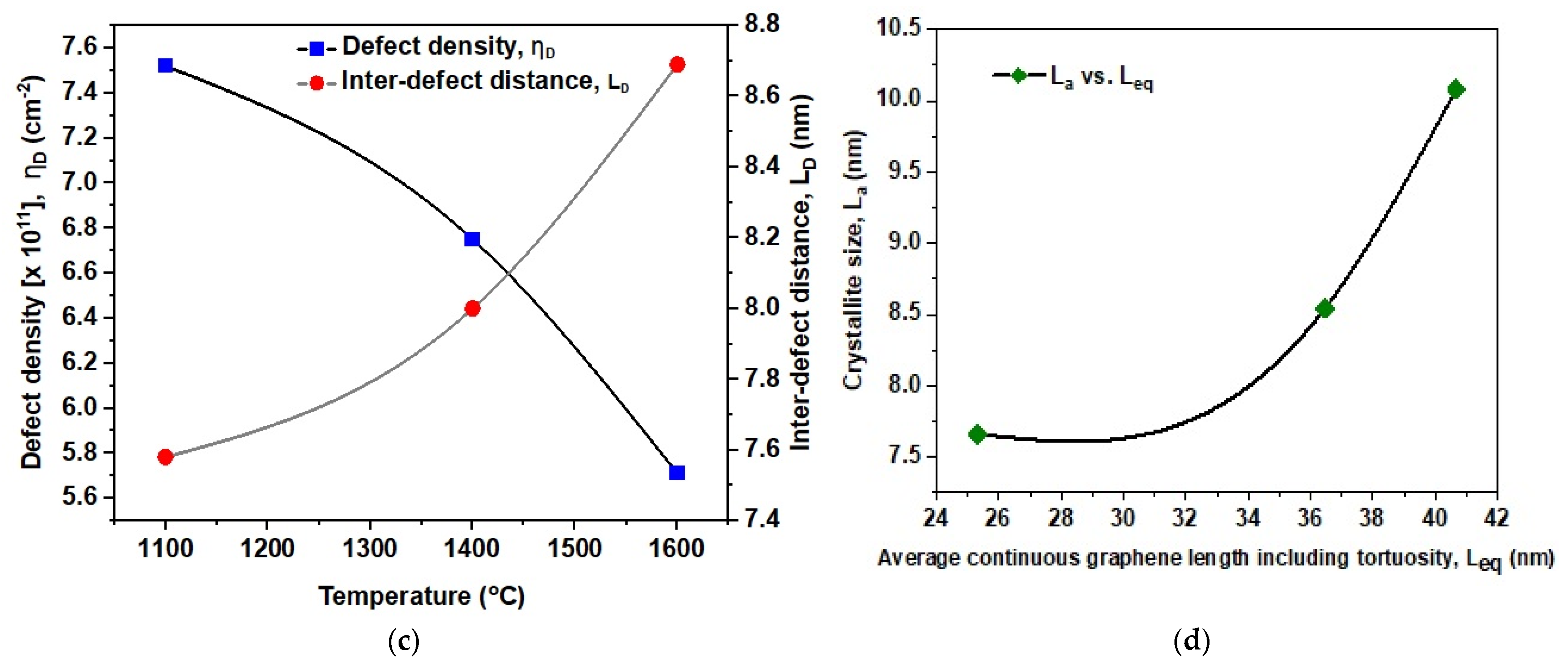
Figure 1. Raman spectra of the C/SiCN nanocomposites showing the carbon phase of various samples represented by the peak position and band parameters: (a) Raman spectrum of the amorphous C/SiCN nanocomposite pyrolyzed at 1100 °C; (b) Raman spectrum of the C/SiCN nanocomposite annealed at 1400 °C; (c) Raman spectrum of the C/SiCN nanocomposite annealed at 1600 °C.
Ceramics 05 00050 g001
Figure 2. Parameters from Raman spectroscopy which determine the evolution of the sp2 hybridized carbon phase in the polymer-derived C/SiCN nanocomposite materials: (a) Dependence of crystallite size (La) and integrated ratios of the D and G bands on temperature; (b) shift of the G band as a function of the pyrolysis temperature; (c) effect of ceramization temperatures on inter-defect distance (LD) and defect density (ηD); (d) growth in crystallite size (La) of the sp2 hybridized carbon with an increase in average continuous graphene length including tortuosity (Leq).
Ceramics 05 00050 g002aCeramics 05 00050 g002b
Figure 3. An XRD pattern of the C/SiCN monoliths fabricated at different temperatures.
Ceramics 05 00050 g003
Figure 4. SEM images and EDS spectra showing the morphologies and energy peaks corresponding to the various elements respectively, of the pelletized C/SiCN nanocomposites pyrolyzed and heat treated between 1100–1600 °C in an argon atmosphere: (a.i) SEM images of the samples pyrolyzed at 1100 °C; (a.ii) EDS spectrum of the sample pyrolyzed at 1100 °C; (b.i) SEM images of the samples heat treated at 1400 °C; (b.ii) EDS spectrum of the sample heat treated at 1400 °C; (c.i) SEM images of the samples heat treated at 1600 °C; (c.ii) EDS spectrum of the sample heat treated at 1600 °C.
Ceramics 05 00050 g004aCeramics 05 00050 g004b
Figure 5. Hall measurement performed in 10 repetitions on the C/SiCN nanocomposites showing the shift in predominant charge carriers from n-type at 1100 °C to p-type at higher temperatures ≥ 1400 °C: (a) Hall coefficients at 1100 °C showing n-type carriers; (b) Hall coefficients of the sample prepared at 1400 °C showing p-type carriers; (c) Hall coefficients of the carbon rich SiCN prepared at 1600 °C showing p-type carriers.
Ceramics 05 00050 g005
Table 1. The carbon phase structure of the carbon-rich SiCN materials.
Parameter/Temperature1100 °C1400 °C1600 °C
Lateral crystallite size, La (nm)7.668.5410.08
Average continuous graphene length including tortuosity, Leq (nm)11.0615.9117.76
Inter-defect distance, LD (nm)7.588.008.69
Defect density, nD, × 1011(cm−2)7.526.755.71
I2D/IG ratio, i.e., stacking number of graphene layer, Lc (nm)1.7 (≤3 layers)1.7 (≤3 layers)1.7 (≤3 layers)
Table 2. The chemical composition of the C/SiCN nanocomposites after pyrolysis.
Pyrolysis TemperatureElemental Composition (wt. %)N/Si (at. %)C/Si (at. %)Carbon Content (at. %)
SiCN
1100 °C39.8748.329.950.502.8364.17
1400 °C41.9152.874.440.212.9570.32
1600 °C43.6153.372.430.112.8671.60
Table 3. Electrical properties of the carbon-rich SiCN materials.
Parameter/Temperature1100 °C1400 °C1600 °C
Electrical conductivity σdc, (S/cm)0.1484.719.26
Carrier density, N (cm−3)6.42 × 10188.45 × 10191.63 × 1019
Carrier mobility, µH, (cm2 V−1 s−1)1.45 × 10−13.52 × 10−13.55
Publisher’s Note: MDPI stays neutral with regard to jurisdictional claims in published maps and institutional affiliations.

