Article

Structural, Optical, Magnetic and Electrical Properties of Sputtered ZnO and ZnO:Fe Thin Films: The Role of Deposition Power

1
Department of Physics and Astronomy, University of Padova, Via Marzolo, 8, 35131 Padova, Italy
2
Department of Physics, Faculty of Science, Ain Shams University, Abbassia, Cairo 11566, Egypt
3
Department of Industrial Engineering, Università Degli Studi di Padova, 35131 Padova, Italy
4
Refractories, Ceramics and Building Materials Department, National Research Centre, Cairo 12622, Egypt
*
Author to whom correspondence should be addressed.
Ceramics 2022, 5(4), 1128-1153; https://doi.org/10.3390/ceramics5040080
Submission received: 14 October 2022 / Revised: 21 November 2022 / Accepted: 28 November 2022 / Published: 1 December 2022
(This article belongs to the Special Issue Ceramic Coatings for High-Temperature Applications)

Abstract

:
Structural, optical, magnetic, and electrical properties of zinc oxide (henceforth, ZO) and iron doped zinc oxide (henceforth, ZOFe) films deposited by sputtering technique are described by means of Rutherford backscattering spectrometry, grazing incidence X-ray diffraction, scanning electron microscope (SEM), UV–Vis spectrometer, vibrating sample magnetometer, and room temperature electrical conductivity, respectively. GIXRD analysis revealed that the films were polycrystalline with a hexagonal phase, and all films had a preferred (002) c-axis orientation. The lattice parameters a and c of the wurtzite structure were calculated for all films. The a parameter remains almost the same (around 3 Å), while c parameter varies slightly with increasing Fe content from 5.18 to 5.31 Å throughout the co-deposition process. The optical gap for undoped and doped ZO was obtained from different numerical methods based on the experimental data and it was increased with the increment of the concentration of Fe dopant from 3.26 eV to 3.35 eV. The highest magnetization (4.26 × 10⁻⁴ emu/g) and lowest resistivity (4.6 × 10⁷ Ω·cm) values of the ZO films were found to be at an Fe content of 5% at. %. An explanation for the dependence of the optical, magnetic, and electrical properties of the samples on the Fe concentrations is also given. The enhanced magnetic properties such as saturated magnetization and coercivity with optical properties reveal that Fe doped ZO thin films are suitable for magneto-optoelectronic (optoelectronic and spintronics) device applications.

1. Introduction

Nowadays, studies on ZO, which is one of the most important 3rd generation semiconductors, support a new stage of comprehensive use due to its multi-functional characteristics. It plays an important role in a very wide range of applications in fields such as: biosensors, biomedical and antibacterial active media, in biological fields [1,2]; UV light-emitting devices, optical waveguides, solar cells in electro-optical fields [3]; transparent high power electronics, varistors, thin film transistors in electronics; gas sensors, water purification and solar photocatalytics in the environmental field [1,4,5]. Moreover, since 2001, many studies have been carried out in the field of Diluted Magnetic Semiconducting Oxides (DMSO) which combine two interesting properties—semiconducting and magnetic—whether to look for a new compound which might be ferromagnetic at room temperature or to find materials which might have a large magnetic moment [6]. The interest in ZO is fueled and fanned by its prospects in optoelectronics applications, having the necessary excellent conditions of ultraviolet and blue emissions because of its unique of chemical and physical properties of a large direct energy gap (e.g., ~3.37 eV at 300 K) and a large exciton binding energy (60 meV) at room temperature which makes it being invaluable compared to numerous other nanomaterials [7]. It is also a promising candidate for semiconductor spintronics applications; Dietl et al. [8] predicted a Curie temperature of >300 for Mn-doped ZO. In addition, n-type doping in Fe-, Co-, or Ni-alloyed ZO was also predicted to stabilize high—Curie—temperature ferromagnetism. Moreover, the well-known room temperature ferromagnetism (RTFM) is one of the more studied phenomena in pure ZO nanostructures doped with magnetic ions. This phenomenon has been found at low temperatures as well, and it has been studied both experimentally and theoretically [9].
Furthermore, the remarkable morphological features of ZO make it a striking material that is widely used as a counterpart of a noteworthy scope of applications. As for ZO’s morphological perspectives, synthesis and fabrication procedures also play an important role. The various parameters used (namely surfactant, temperature, concentration, and time, etc.) play a crucial role in the growth of various forms of synthetic processes. An enormous number of different methods for the synthesis of surface structured ZO as nanopowder, composites, and films have been published worldwide. There are widely noted techniques for synthesizing different ZO nanomaterials, composites and doped heterostructures, including precipitation, wet-chemical technique, sol-gel procedure, hydrothermal method, solvothermal procedure, sputtering, coating and microwave techniques, etc. [1].
For several of the above-mentioned applications, a stable, high, and reproducible p-doping is mandatory. Though progress has been made, this aspect still represents a major problem. The contribution of the current ZO research is not only on the same topics as earlier, but also includes nanostructures and nanotechnologies, new growth and doping techniques, and focuses more on the application-related aspects of daily life [9,10].
In this study we planned to control and enhance the optical band gap, and the magnetic properties of Zinc Oxide (ZO) thin films doped by a transition element (TM).
Fe is a magnetic transition metal that has several oxidation states, an electronegativity of 1.83 and ionic radii that range from 0.61 to 0.78 Å (depending on the magnetic and oxidation states) [10]. Because the properties of iron are similar to those of aluminum or gallium, it is considered a potentially attractive alternative for the doping of ZO thin films [11]. However, the performance of iron as a dopant is complicated by the existence of 3d electrons in its electronic configuration. Currently, most studies on Fe-doped ZO thin films focus on their wide applications. As we are aware, fewer reports have investigated Fe-doped ZO thin films as transparent conducting oxides [12,13,14]. Due to the complex electronic structure of iron, it has been difficult to control the different properties of these films. Moreover, iron-doped ZO thin films have been synthesized by several techniques including electrodeposition, spray pyrolysis, spin coating, ion implantation, and the sol–gel method. Sputtering is the most widely used technique for the preparation of Fe-doped ZO thin films [15] because it provides the ability to control the properties of the films through several deposition parameters, such as the sputtering mode, power, sputtering and reactive gas pressures, substrate temperature, and target composition and allows deposition of different materials [16]. Three sputtering techniques have been used to synthesize Fe-doped ZO thin films:
  • simultaneous co-sputtering from two targets (ZO and Fe) [17];
  • direct-current (DC) sputtering using an Fe-doped Zn target [18] or a Zn target with Fe pieces attached to it [19] and;
  • radio-frequency (RF) magnetron sputtering.
Several of the studies using RF-sputtering for Fe-doped ZO thin film have investigated the effect of doping concentration on the properties of the films [17]. Others have studied the influence of the deposition parameters on the properties of films with fixed dopant concentrations [19].
In this present study, a thin film of iron (Fe) doped zinc oxide (ZO), with various Fe-concentrations, is investigated using RF-magnetron sputtering on silica and silicon substrates. We report the influence of the Fe doping on the microstructure, optical, magnetic and electrical resistivity of the ZO films. The results indicated that ZO film with 5.0 at. % doping-concentration can attain a higher energy gap and magnetic properties, and better electrical resistivity.

2. Materials and Methods

Undoped and doped ZO films with Fe were deposited on single-crystal n-type Si (100) wafer and silica (HSQ 100 from Heraeus) glass preliminarily washed in piranha solution for magnetron sputtering. The ZO target (99.95% purity, 100-mm diameter) is placed in a radio-frequency driven (RF) source while setting the power at 100 W and Fe target in a direct current (DC) source providing powers of 3, 5, 10, and 15 W to produce (1, 2.4, 4.8, 5) at. % of Fe, respectively. Moreover, in order to control the sputtering yield of Fe and instead of reducing the DC power (which produced instabilities of the DC source), we performed the DC sputtering through a grid with a different mesh size to block part of the Fe atoms. During the deposition, the substrate was rotated at a low speed to enhance the thickness uniformity of deposited films. The two sources were tilted of an angle 30° with respect to the axis normal to the sample surface allowing a simultaneous deposition of the two targets and the source-target distance was about 15 cm. The thickness and the composition of the films were properly tuned through an optimized combination of the electrical power of the source and the opening time of the shutters placed in front of the targets. The thickness of the films was 150 nm, which was controlled by the deposition time. Other detailed conditions about the deposition process of the films are summarized in Table 1.
Furthermore, the film thickness was measured using a thickness profile-meter and by Rutherford back scattering (RBS), performed with a HVEC 2.5 MeV Van de Graaff accelerator at Legnaro National Laboratory (LNL)—INFN, using 2 MeV α -particles at normal incidence and a scattering angle of 20°, which was also used to determine the contents by atomic percentage of Zn, O and Fe ions. Furthermore, the hexagonal phase wurtzite structure of samples was confirmed by grazing incidence X-ray diffraction (GIXRD) (Philips X’Pert PRO MRD triple axis diffractometer (angular resolution 0.01°, accuracy 0.001°)) and the scanning electron microscope (SEM), Zeiss Field-emission SEM (FE-SEM), was used to determine the surface morphology. The optical properties of the films were measured using UV-Vis optical spectroscopy, Jasco V-670 UV-Vis-NIR Spectrophotometer with working range 190–2500 nm, in order to determine the optical parameters such as band gap, Urbach energy and refractive index for all investigated samples.
Likewise, the magnetic hysteresis loops for the doped and undoped films were investigated by a vibrating sample magnetometer (VSM) (LakeShore model no. 7410 USA) in a maximum applied field of 20 kOe. Finally, the IV characteristics and electric resistivity was also measured for undoped and doped films by a two probe method with a KEITHLEY 6514 system electrometer. For simplicity, throughout the present work, the “balanced stoichiometry” for the Fe doped ZnO will be named ZOFe. The DC power values are indicated as follows: ZOFe/3 W, ZOFe/5 W, ZOFe/10 W and ZOFe/15 W for 3, 5, 10 and 15 Watt for DC deposited power of the Fe source target.

3. Results

3.1. Elemental Analysis

The elemental composition of ZO and ZOFe films was measured by Rutherford backscattering spectrometry (RBS). The RBS data analysis is reported in Figure 1 where the experimental data for all investigated films is superimposed to the simulation. The quality of the fit is the direct proof of the sample homogeneity.
One can notice that the surface edge for the different elements (Zn, O, Si and Fe) can be observed clearly from Figure 1. The large peak on the right-hand side located in the high energy range of the spectrum is due to the zinc atoms whereas the low energy peak signal is related to the oxygen, which is superimposed over the continuous spectrum of a Si substrate. Moreover, small peaks were observed on right-hand side of the Zn peak which indicate the Fe. The yield account of these peaks increased with increase in the DC power value in the co-deposited process from 3 W to 15 W.
RBS is not equally sensitive to various elements. The height of the RBS signal depends on the scattering cross section which is proportional to the square of the atomic number of the element. Thus, for light elements, the RBS signal is much lower than for heavy ones [20]. Therefore, it is quite difficult to separate the signal from such elements as nitrogen, carbon or oxygen, from the high background of much heavier substrates as Si. Consequently, it is not easy to evaluate the contribution of light elements. Zinc, oxygen and iron contents in the ZO and ZOFe thin films were evaluated from the RBS random spectra. It has been found that the value O: Zn content is approximately equal 1 and the results are summarized in Table 2.

3.2. GIXRD Analysis

Figure 2 depicts the GIXRD pattern of the ZO thin films. One can see that it exhibits a hexagonal crystal phase, which was confirmed with a standard JCPDS card (PDF No. 36–1451). In the GIXRD pattern, the two dominant peaks, (002) and (103) were obtained for all films without any secondary phase.
All films exhibited preferential (002) c-axis orientation, which grew perpendicular to the substrate surface. This can interpreted as follows: the sputtered ZO and ZOFe thin films with a c-axis have a preferential orientation due to the lowest surface free energy of (002) plane in ZO. In the equilibrium state, the films grow with the plane of the lowest surface free energy parallel to the surface if there is no effect from the substrate. Additionally, the sp3 hybridized orbit in zinc oxide forms a tetrahedral coordination. Because each apex is parallel to the c-axis in the wurtzite structure, ZO films prefer to grow in the (002) direction [21].
Table 3 represents some significant data estimated from the diffracted peaks such as 2θ, d-spacing, (hkl), peak intensity, crystallite size, and the texture coefficient for all deposited films.
The texture coefficient TC(hkl) is another perspective for preferred orientation and/or preferred growth. TC(hkl) can provide quantitative information on the preferred crystal orientation which can be calculated from the expression [22,23]
T C ( h k l ) = I ( h k l ) / I o ( h k l ) ( 1 / n )   n I ( h k l ) / I o ( h k l )
where I(hkl) is the measured intensity and Io(hkl) is the standard JCPDS intensity and n is the number of diffraction peaks. If TC(hkl) ~ 1 for all the (hkl) planes considered, then the films have a randomly oriented crystallite similar to the JCPDS standard, while values higher than 1 indicate the abundance of grains in a given (hkl) direction.
Values 0 < TC(hkl) < 1 indicate the lack of grains oriented in that direction. As TC(hkl) increases, the preferential growth of the crystallites in the direction perpendicular to the hkl plane is the greater. Since two diffraction peaks were used ((002) and (103)), the maximum value TC(hkl) possible is two.
The calculated texture coefficient results are displayed in Table 3 and were found to be maximum for the (002) plane and increased by increasing iron content, as shown in Figure 3. Moreover, the (002) polar facet of Fe doped ZO films increased significantly compared to the (103) facet. This also indicates the preferential growth along the c-axis orientation.
On other side, the crystallite size may be estimated from the full-width at half-maximum (FWHM) of (002) and (103) diffraction peak using the Debye–Scherrer formula [24] which is expressed as:
D = 0.9   λ β   c o s θ h k l
where D is the average crystallite size, λ is the wavelength of the X-ray and takes 1.54 Å for Cu Kα, β is the peak width of two peaks at half maximum height (FWHM) in radians, and θhkl is the diffraction angle of the crystal plane (hkl). The values of the average crytallite size are given in Table 3.
In addition, using the interplanar spacing values (d-spacing) and the related hkl parameters for hexagonal systems, the lattice parameters ( a , b , and c where a = b ) of the wurtzite cell of ZO and ZOFe thin films have been calculated by using following formula [22,25]:
1 d 2 = 4 3   ( h 2 + h k + k 2   a 2 ) + ( l 2 c 2 )
Interplanar d-spacing is calculated according to Bragg’s law:
n λ = 2   d ( hkl ) Sin   θ
where d is lattice spacing, a and c are lattice constants, h, k, l are miller indices, θ is the angle of corresponding peak and λ is the wavelength of X-ray used (1.5402 Å). Considering Bragg’s law, it is possible to rewrite Equation (4) as follows:
4 sin 2 θ λ 2 = 4 3 ( h 2 + h k + k 2 a 2 ) + ( l 2 c 2 )
There are two unknowns to be calculated in the formula above. Because of this, while calculating lattice constant a , a peak in the form of (h00) should be used to eliminate c from the equation. As an alternative, the (00l) peak should be used to get an equation with just one unknown for calculating the c constant. Following correct peak selection, the following equations for a and c constants are obtained [25,26].
a = λ h 2 + h k + k 2 3 sin θ
c = λ l 2 sin θ
The calculated lattice parameters for all films are listed in Table 4. As can be seen from Table 4, the a parameter remains almost the same, while the c parameter varies slightly due to an increase in Fe content throughout the co-deposition process. As we noticed from XRD, no obvious peaks corresponding to iron metal or iron oxide phase were observed. Furthermore, the wurtzite structure of ZO remained unchanged after iron modification. There is a slight left shift in the (002) and (103) peaks of the ZOFe films which could be interpreted as follows. Fe exists stably in both valence states, i.e., Fe2+ and Fe3+ state. The peaks would shift towards a lower angle if Fe exists in Fe2+ (0.78 Å) state due to its larger ionic radius than Zn2+ (0.74 Å), as seen in Figure 4. This confirms that iron has been doped into the ZO lattice. However, if it exists in the Fe3+ (0.68 Å) state, the peak shift will occur towards the higher angle side. As a result, we may conclude that the iron in our samples is predominantly in the 2+ state.
As well, the volume V, the internal parameter U, and the bond length L of wurtzite unit cell for hexagonal ZO and ZOFe thin films have been calculated using the following expressions [22,25,27]:
V = 3 2 a 2 c ;   U = 1 3 ( a 2 c 2 ) + 1 4 ;   L = [ c 2 ( 1 2 U ) 2 + a 2 3 ] 1 / 2
The obtained values are tabulated in Table 4 and the variation in a , c and L after Fe incorporation may be attributed to the differences between the atomic radii of the host material (ZO) and the dopant (Fe) [27].
Moreover, the average uniform strain, ezz, in the lattice along the c-axis in the randomly oriented ZO and ZOFe films has been estimated from the lattice parameters as follow:
e z z = c c 0 c 0
where c is the lattice parameter of the ZO film calculated from the (002) peak of XRD pattern and the c0 is the lattice parameter for the ZO bulk. For hexagonal crystals, the stress (σ) in the plane of the film can be calculated using the biaxial strain model [28,29]:
σ = [ 2 C 13 ( C 11 + C 12 ) C 33 C 13 ] e z z
where Cij are elastic stiffness constants for ZO, (C11 = 2.1 × 10¹¹ N/m2, C33= 2.1 × 10¹¹ N/m2, C12 = 2.1 × 10¹¹ N/m2, and C13 = 2.1 × 10¹¹ N/m2). This yields the following numerical relation for the stress derived from the change in the ‘c’ lattice parameter:
σ ( N m 2 ) = 4.5 × 10 11 e z z
The calculated values of stress (σ) in the undoped and doped films are listed in Table 4. The negative sign indicates that the films are in a state of compressive stress which not seen in pure ZO film. The total stress in the film typically consists of two components: intrinsic stress which introduced by impurities, defects and lattice distortions in the crystal, and the extrinsic stress familiarized by the lattice mismatch and thermal expansion coefficient mismatch between the film and substrate. When the thickness of a thin film is large, the extrinsic stress in the thin film normally relaxes. All of the films in our current study have a thickness around 150 nanometers. As a result, extrinsic stress will be absent, and the overall predicted stress values will be dominated by intrinsic stress. Furthermore, in the current scenario of sputtering deposition with rising DC power, this intrinsic stress arises as a result of the bombardment of energetic species. Strong compressive stress is present in films deposited at lower temperatures. In the sputtering process, the highly energetic species could be implanted below the ZO surface, causing high intrinsic stresses by creating the defects [29,30]. The existence of stress in the ZO films was reported by Gupta and Mansingh, who ascribed it to oxygen interstitial defects [31]. It is well known that, because of the higher formation energy, the oxygen interstitials are less expected in ZO films. In the present experiment all the films were deposited in argon atmosphere. So, the possibility of the formation of oxygen interstitials is ruled out and the formation of Zn interstitials and the oxygen vacancies are expected. Thus, in our case, the intrinsic stress in the deposited ZO and ZOFe films seems to arise due to presence of Zn interstitials.

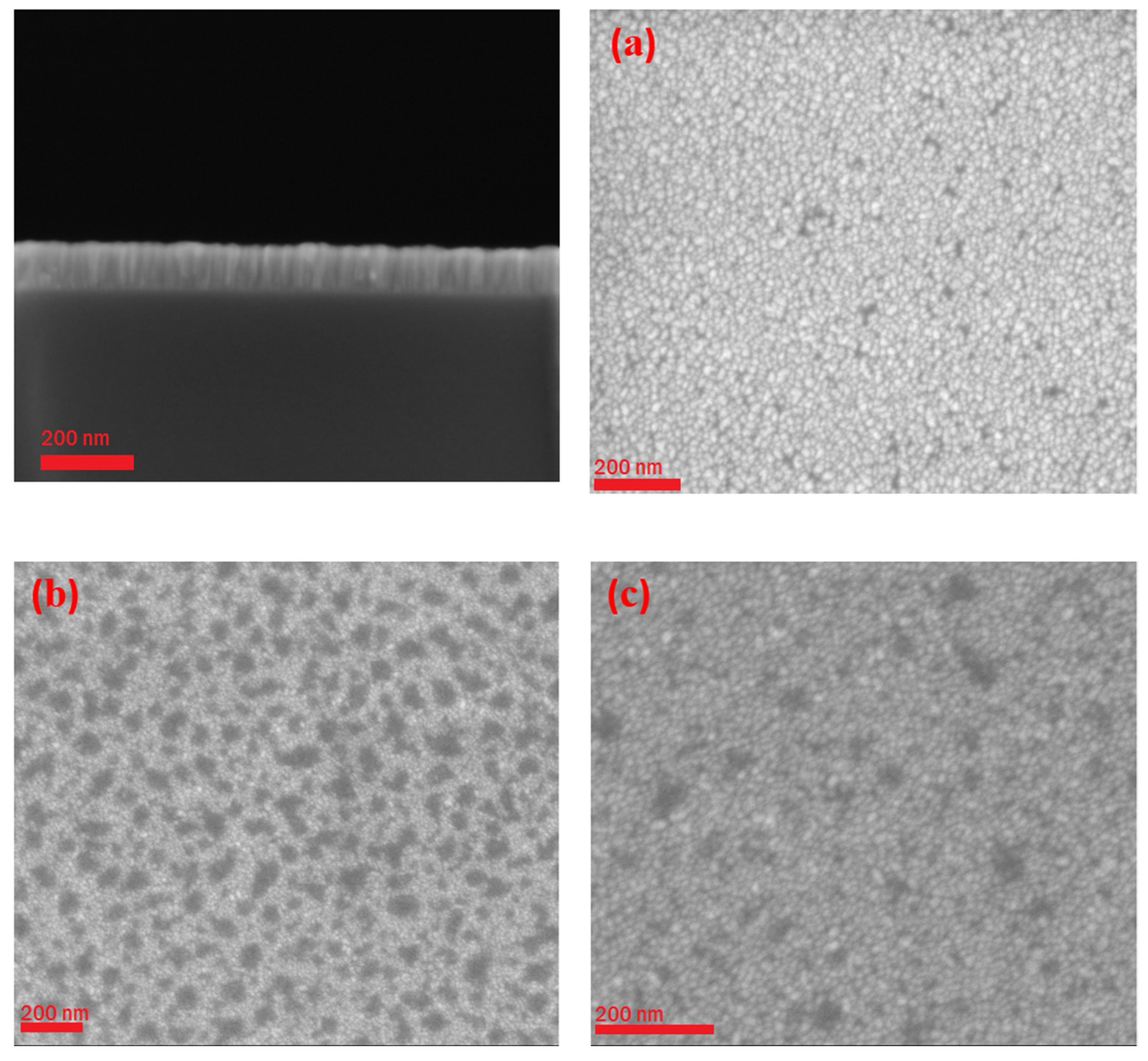
3.3. Microstructural Analysis

Figure 5 shows the morphology of the ZO and Fe doped ZO thin films; the pure zinc oxide film surface seems to be agglomerated, spherical in shape as shown Figure 5a. The surface of the films consists of tightly packed grains forming a smooth surface without any voids and cracks whereas the Fe doped zinc oxide films in Figure 5b,c look like black and white islands of spherical shape. Still, by increasing the DC deposited power for Fe with ZO deposition, the black spots decreased. A SEM image of the sectional view of the samples could help in discovering the shape of the spherical grains and their interface with the substrate as in Figure 5. Moreover, the shape of the grains would be hard to identify because the growth could not be described in a reliable way. Further, the distribution and size in grains is inhomogeneous. Figure 6 shows the EDX spectrum of the ZO and Fe doped ZO thin films. The observed peaks are attributed to zinc, oxygen and iron as principal elemental components with no other impurities being obtained. The Zn:O:Fe atomic percentage ratios of the ZO thin film are listed.

3.4. Optical Properties

3.4.1. Transmittance Spectra

Zinc oxide and iron doped zinc oxide samples grown on SiO2 are transparent to visible and NIR light; thus it was possible to obtain transmittance spectra and make observations on the material properties. The spectra were taken in the range between 300 and 900 nm, as shown in Figure 7. The optical transmittance spectra of the films show a good transmission in the visible region and a sharp fall in the UV region which corresponds to the band gap. The decrease of the transmittance is due to the interaction of the incident long-wavelength radiation with the free electrons in the films [32]. Moreover, the films have good transmission in the visible region of the spectrum terminated at shorter wavelengths while, in the UV region, the obvious absorption could be observed; it increased with increasing Fe content.

3.4.2. Optical Band Gap

The energy gap and refractive index of semiconductors are two essential physical parameters that define their optical and electronic properties. The optical energy gap (Eg) determines the threshold for absorption of photons in a semiconductor. In order to determine the optical energy gap (Eg), there are several numerical methods based on the experimental data. We are used different methods and compared them to obtain (Eg) values which have a good agreement with the literature.
(A)
Tauc method:
In most of the literature, the energy gap in the crystalline and amorphous semiconductors is determined by the Tauc method [33]. This method is easy to apply due to fitting of the linear function to the graph for parameter: m = {0.5, 1.5, 2, 3} which represents direct allowed, direct forbidden, indirect allowed and indirect forbidden optical transition, respectively. The energy gap determined using the Tauc method is often subject to high uncertainty. In some cases, it is possible to fit a straight line for all values of parameter m. The energy gap of all the films is determined from the absorption coefficient (α) which can be calculated from the transmittance (T) of the undoped and doped ZO thin films. The absorption coefficient (α) is calculated from Equation:
α = ( 1 d ) l n ( 1 T )
where (d) is film thickness and (T) is the transmittance. The absorption edge was analyzed by the following Equation:
( α h ν ) 2 = A ( h ν E g )
where A is a constant, is the incident photon energy and Eg is the optical energy band gap. Based on Equation (15), the plots of (αhν)2 as a function of incident photon energy () were obtained for the undoped and doped ZO thin films and are shown in Figure 8. The linear portions of these plots are extrapolated to meet the energy axis and the energy value at (αhν)2 = 0 gives the values of the energy gap Eg for the thin films. The Eg values are listed in Table 5.
(B)
The derivative of transmittance (T) against photon energy ()
This method is applicable for transitions between direct band gaps [34]. The transmission through a film may be approximated as:
T ( E ) [ 1 R ( E ) ] 2 e α ( E ) d
where E is the energy of the incident light, R is the reflectance, and d is film thickness.
α ( E ) = C E η r ( E ) E E g
where C is a constant and ηr(E) is the energy-dependent index of refraction. The behavior of the reflectance at the band gap energy must be considered while calculating the transmission derivative. It can be shown that as EEg, the quantities (1 − R(E)) and dR(E)/dE remain finite at energies in the environs of Eg due to the presence of a band tail that prohibits singularity- type behavior. The reflectance and its derivative are well-behaved values near the band gap energy, according to experimental studies concerning ZO thin film properties [35]. As a result, we can write the transmission through a direct gap semiconductor as
T ( E ) = e C d ( 1 / E η r ( E ) ) E E g
After taking the first derivative of T(E) with respect to energy and then at the limit EEg, this results in a spike towards negative infinity at E = Eg. Due to band tail states, it was assumed that dηr(E)/dE is continuous around Eg. As a result, when plotting dT/dE versus E, a significant singularity will appear at the band gap energy. In realistic instances, absorption tails exist, which soften the divergence and create well-defined peaks around the gap energy, as also can be seen in Figure 9 for ZO and ZOFe/10 W thin films. The values of the band gap of all investigated samples obtained by the derivative method are listed also in Table 5. These values of band gap are very close to the values obtained by Tauc method. Discrepancy between values of band gap obtained by both methods can be explained: the fitting of a line in the linear region of (αhν)2 is quite challenging which adds errors in determination of the band gap. Hence, the derivative method is considered more appropriate when compared to Tauc method.
lim E E g d T d E = C ( 0 0 + 1 0 )
(C)
The derivative of transmittance (T) against wavelength (λ)
As we noticed in the transmittance curve of ZO films, there are transmittance tails at the high energy side of the absorption edge. Because a sharp absorption edge is generally observed in the transmittance spectra of direct band gap semiconductor films, we computed the derivative of transmittance (T) against wavelength (λ) in an effort to accurately determine the optical band gap of undoped and doped ZO films. The sharp absorption edge in the transmittance spectra may result in a sharp peak in a plot of dT/dλ vs. from which the optical band gap can be successfully determined. Figure 10 shows plots of dT/dλ vs. for the ZO and ZOFe/10 W thin films. One can see in Figure 10 a broad peak centered around 3.3 eV, corresponding to a band gap of all investigated films, also listed in Table 5.
(D)
Logarithmic derivative (LD) method:
This approach combines the advantages of both the Tauc [33] and McLean [36] methods: the fit is linear, and the parameter m is calculated as a consequence of the fitting. Significantly, the results of all three approaches are consistent in simple cases.
As we referred above, the Tauc method is based on linear fit for αhν1/m data for selected m = {0.5, 1.5, 2, 3} values. The zero point of the fitted linear function is then the energy gap Eg. In the McLean method, one can determine m, Eg and parameter A in Equation (13) by fitting a power function to αhν data. LD transformation starts from the Tauc equation. For the sake of calculating the natural logarithm, let us suppose that all the quantities in Equation (13) are unitless. Then the natural logarithm will be:
l n ( α h ν ) = m   l n ( A ) + m   l n ( h ν E g )
By differentiation of Equation (18) with respect to
d   l n ( α h ν ) d ( h ν ) = m   ( 1 h ν E g )
The left side of Equation (19) is calculated based on the experimental data. This numerical derivative should be calculated as the difference of transformed measurement data (, αhν) from subsequent measurement steps.
Now, we can determine the precise value of the optical band gap from the d   l n ( α h ν ) d ( h ν ) vs. curve as in Figure 11. We can see that a peak in the curve appeared at the band gap energy (Eg); i.e., = Eg. The peak at a particular energy value gives the approximate optical band gap, Eg [37].
On other hand, the type of the optical transition can be estimated from the slope (m) of the curve of ln (αhν) vs. ln (Eg) using the Eg value of the highest Fe concentration doped ZO (15 at. %), as an example, and to determine the value of (m) which was found about 1/2 from the slope as shown in Figure 12. This indicates that the optical transition through the base glass and also the doped samples is a directly allowed transition which we selected to obtain Eg values by using the Tauc relation.
Thus, the estimated values of Eg for ZO doped and undoped by Fe are listed in Table 5 to compare with the other values obtained from different approaches.
One can see that in Table 5, the obtained values of Eg determined from the Tauc method are close to those determined by dT/dE and dT/dλ and LD methods. Furthermore, the average values of the Eg are 3.26, 3.27, 3.29, 3.33 and 3.39 eV for the undoped and 3 W, 5 W, 10 W and 15 W of Fe-doped ZO thin films, respectively.
It is worthwhile to notice that two points may be inferred from these energy gap values. The first is that from the undoped to doped thin film, the Eg values increased. Furthermore, as the doping concentration of Fe increases, the Eg value increases.
The first point can be interpreted as follows. As we know, the incidence of a photon with energy of on a semiconductor leads to a transition between the highest occupied state of valence band and the lowest unoccupied state of the conduction band. This phenomenon is applied to calculate the optical band gap energy of ZO thin films as we referred before. In Fe-doped ZO thin films, the optical band gap energy mainly depends on the valence state of Fe ions [38,39]. With Fe-doped ZO thin films, there is a large variability in the optical behavior which leads to inconsistent conclusions. The valence state of Fe is an important factor in the optical properties of ZO thin films. Fe dopants in ZO thin films can be in the two forms of Fe2+ or Fe3+, or even coexistence of these two forms is seen. By addition of Fe into ZO films, the maximum of the valence band is increased and the minimum of the conduction band is decreased which leads to the reduction of band gap. However, substituting Fe3+ ions into Zn2+ leads to providing extra free carrier concentrations. As a result, the Fermi level moves toward the conduction band and the band gap increases. This makes the optical band gap of Fe-doped ZO thin films tunable.
Moreover, it is known that doping significantly alters the absorption spectrum of the pure semiconductor, resulting in degenerate energy levels which cause the Fermi level to push above the conduction band edge. This shift is known as doping induced band-filling called a Moss–Burstein shift and leads to an increase in the band gap from the undoped to doped thin film [40]. In addition, with Fe incorporation, there are initially sp-d exchange interactions that do not strongly affect the band gap. After a further doping percentage, the Moss–Burstein effect dominates the normal sp—d exchange interactions. In addition, ZO is normally n-type material stable at room temperature in which the Fermi level lies in the conduction band when doped with greater Fe [41]; as a result, there is an increase in the band gap with more Fe doping. Since no empty state is available inside the conduction band, so the absorption edge shifts towards the higher energy region, thereby giving rise to an increase in the band gap. With increasing Fe doping the d—d transition of Fe ions also increases and leads to increase in the band gap. According to Parra-Palomino et al. [38], increasing Fe doping concentration to ZO nanocrystals increased the band gap significantly. Chen et al. [42] and Wang et al. [43] found that raising the Fe doping concentration in ZO films can minimize the band gap.

3.4.3. Urbach Energy

One of the main properties which measure the degree of structural disorder in the films is the Urbach energy (EU). The imperfection in the structurally disordered film leads to broadening the bands of localized states. As we mentioned, near the band edge, the absorption coefficient has an exponential dependence on photon energy. This dependence is given as follows:
α = α o e x p ( h ν E U )
where αo is the band tailing parameter that can be obtained by:
α o = σ o ( 4 π c ) x Δ E
where σo, c and ΔE are the electrical conductivity at absolute zero, the velocity of light and the width of the tail of localized states in the energy gap, respectively, and x = 0.5 for the directly allowed transitions [44]. Then the Urbach energy can emerge from Equation (22) as:
E U = [ d   ( l n ( α ) ) d   h ν ] 1
As shown in Figure 13, the values of the EU were obtained from the slopes of the linear fitting of the plots of ln (α) versus () and are listed in Table 6. EU increases from 225 to 403 meV as the Fe concentration increased. The dopant may contribute significantly to the width of localized states within the ZO’s optical band. In other words, the EU is responsible for the valence and conduction bands’ tails [45]. Moreover, EU values confirm the GIXRD analysis which shows that Fe doping is followed by an increase of the strain which can also create structural disorder.

3.4.4. Refractive Index

The two most interesting optical properties of a semiconductor are the absorption edge, or optical energy gap, and the refractive index. The relation between the optical band gap Eg and the refractive index no was proposed for first time by Moss in 1950 on the very general grounds that all energy levels in a solid are scaled down by a factor 1 / ε o p t 2 , where ε o p t = n2 is the optical dielectric constant; it was described in detail elsewhere [46,47]. Moss showed that the energy levels of the semiconducting materials can be scaled down by the term 1/n4 as follows [46]:
n o 4 E g = 9   eV
Then Ravindra and Srivastava [48] modified Equation (25) to be:
n o 4 E g = 108   eV
The main difference between the Moss and Ravindra relations originated from the estimating of the reflection loss by Ravindra. Moreover, Equation (26) covers most of the semiconducting materials used for solar cell, photocatalytic and sensing applications. Dimitrov and Sakka [49] have deduced the correlation between the refractive index and the optical band gap from the Lorentz- Lorentz (L.L.) Equation:
n o 2 1 n o 2 + 2 = 1 E g 20
The estimated refractive index based on the optical band gap is shown in Table 6. The refractive index of ZO was compared with the optical data from references [22,49]. As we can see, by increasing the Fe content, the refractive index decreased and as we know the refractive index is correlated to the optical band gap. Subsequently, from Equations (25) and (26), the relation between them is inverse.

3.4.5. The Extinction Coefficient

The extinction coefficient (k) reflects the absorption of electromagnetic waves in the semiconductor due to inelastic scattering events and it can be calculated from the transmittance spectra using the relation
k = α λ 4 π
The dependence of k on the wavelength for all investigated thin films is shown in Figure 14. In the UV region (λ < 400 nm), the k value increases from 0.36 to 0.42 with increasing Fe concentration. Furthermore, the k values are very small and relatively constant in most of the visible region. This indicates the smoothness on the surface and homogeneity of the films and enhances its uses in blocking UV radiation [40]. As well, increase in k value by doping Fe can be ascribed to increasing topical donor levels formed within the energy levels that lead to an increased extinction coefficient, showing that the electronic transitions occur directly.

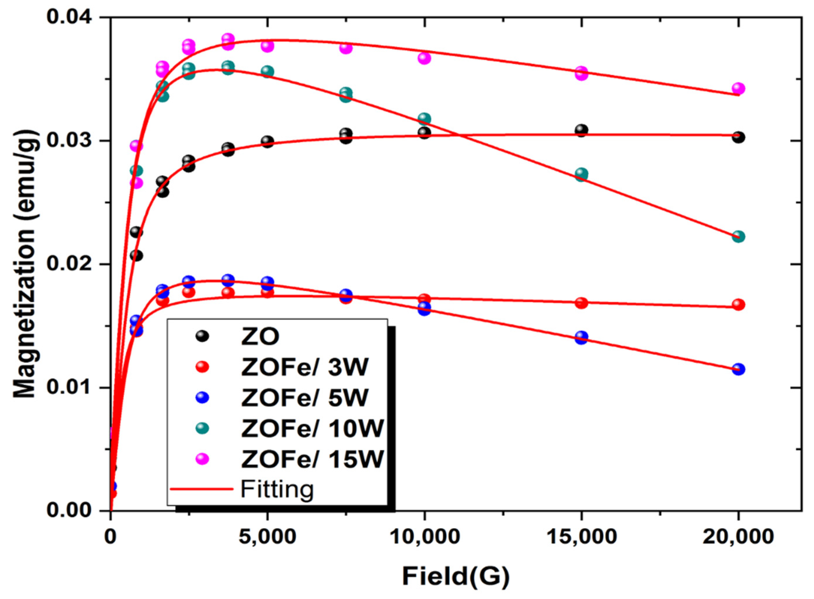
3.5. Magnetic Properties

3.5.1. Magnetic Behavior of the Films

The hysteresis loops of ZO and Fe doped ZO thin films in Figure 15 show clear room temperature ferromagnetism (RTFM) for all the doping concentrations of Fe; they were obtained from room temperature vibrating sample magnetometer (VSM) measurements. It is clear from Figure 15 that undoped ZO and Fe doped ZO films show well-defined hysteresis loops with noticeable coercivity. The loops are S-shaped, which indicates the ferromagnetic nature of the samples. One can notice that there is non-saturation of the M-H loop at higher applied fields, which is a commonly observed phenomenon in semiconductor/metal nanocomposites. Rumpf et al. also observed such non-saturation behavior for ferromagnetic semiconductors and attributed it to the lattice defects and magnetic anisotropy [50].
The mechanism of RTFM in the ZO based system was still unclear for researchers. The dopant related secondary phase, magnetic cluster, metal precipitation formation will lead to magnetic behavior in the doped ZO. In a doped ZO system, the carrier exchange interactions such as RKKY, indirect double exchange interactions and super exchange interactions induced a magnetic nature [51,52,53]. In addition, the doped and co-doped ZO samples reveal ferromagnetism at RT due to the presence of intrinsic lattice defects. The presence of lattice defects as strain and texture, and concentration of Fe doping ions may also have a major impact on the room temperature magnetic properties [54,55]. Generally, RT ferromagnetism in TM doped ZO films could be explained on the basis of intrinsic and extrinsic effects associated with the local magnetic moments. If the spin of Fe ions has an exchange interaction with local magnetic moments of ZO then it is intrinsic effect. When there is a direct interaction between the local magnetic moments of the Fe clusters, it is known to be an extrinsic effect.
Accordingly, in Figure 15, the M-H curves of the pure ZO exhibit ferromagnetic (FM) behavior and Fe doped ZO thin films, with Fe concentration 2.4, 4.8 and 5 at. % of Fe dopants, exhibit diamagnetic behavior at a high magnetic field and FM behavior in the lowest field regime. There are several literature reports that pure ZO exhibited ferromagnetic nature at room temperature due to the exchange interaction between localized electron spin moments resulting from oxygen vacancies [56].
For more details about the diamagnetic behavior shown in the pure ZO films, a fitting with Langevin curve was performed, as shown in Figure 16; this type of analysis has been conducted on ZnO doped with transition metals [9].
Further, the ferromagnetic property for DMSs can be contributed from the secondary phase related to metal oxides or metal clusters with a ferromagnetic property. DMSs could have an intrinsic effect as well [57]. However, our GIXRD patterns clearly indicate the absence of clustering of metallic iron phase or iron oxide cluster in the films. Moreover, the possibility of attributing the observed ferromagnetic order of Fe doped ZO thin films to the carrier-mediated mechanism or RKKY exchange interaction is also ruled out because the DMSs usually show very high resistance. Therefore, RTFM of our Fe doped ZO films are not due to the carrier-mediated mechanism. A pertinent and appropriate explanation for the observed RTFM [58] in our case is the ferromagnetic exchange mechanism involving oxygen vacancies model. This could be explained in terms of two reasons: (1) the number of oxygen vacancies (OV) and zinc interstitials (Zni) and (2) the exchange interaction between doped transition metal ion and O ion spins.
Further, Kittilstved et al. [59] stated that the ferromagnetism in TM doped ZO is due to the effective dopant defect hybridization arising from the energetic alignment of the shallow donors, Zn interstitial (Zni) and oxygen vacancy (OV), with TM+/2+ level. Thus, the magnetic coupling between Fe ions with ZO is FM mediated by (Zni) and (OV) and this may account for the observed RTFM and indicates that defects play a role to gain a FM coupling. In addition, in our case, for low magnetic fields, the ferromagnetic behavior can be attributed to the presence of small magnetic dipoles located at the surface of thin film nanocrystals, which interact with their nearest neighbors inside the crystal involving oxygen vacancies [53].

3.5.2. The Magnetic Parameters

Table 7 shows the saturation magnetization Ms of undoped ZO~9 × 10⁻⁴ emu/g at 2000 G. Vettumperumal et al. [60] have observed RTFM of ZO thin film with Ms value ~ 6.9 × 10⁻⁵ emu/g emu/g at 300 K while Ariyakkani et al. [61] have obtained Ms value ~ 5.6 × 10⁻⁵ emu/g at 300 K for ZO thin film. Therefore, the magnetization value obtained in our work is higher as compared to previous reported values of undoped ZO. Furthermore, it is obvious, from Table 7, that the saturation magnetization of the films is increased by increasing the Fe concentration. As we mentioned before, the origin of ferromagnetism in transition metal doped ZO until now is still not clear. A number of studies indicate that ferromagnetism in transition metal doped ZO may come from secondary magnetic phases [62]. However, others reported that the RTFM in Fe-doped ZO could be due to the oxidation of Fe in mixed valence (Fe2+ and Fe3+) states [63]. The exchange interaction between conductive electrons and local spin polarized electrons is responsible for the magnetic behavior of Fe-doped ZO. Likewise, the occurrence of Fe-Fe super exchange interaction could be one reasons for increased Ms values with increasing Fe concentration; it is found to be dominant at higher Fe doping concentrations [64,65].
The coercivity of Fe doped films is lower than the undoped film at any particular Fe concentration, as shown in Table 7. There are several factors influencing the reduction in the coercivity such as magnetic domain size, micro-strain, magnetocrystalline anisotropy, and shape anisotropy. However, such decrease in coercivity could be related to a decrease in the anisotropy field, which reduces the thickness of the domain wall [66]. However, the coercivity (Hc) is low (~95 Oe) for the doped films and it indicates that all Fe doped ZO thin film samples are ferromagnetically soft compared to ZO. The magnetization measurements by Kumar et al. [63] on 1% Fe doped ZO samples shows soft ferromagnetic behavior at room temperature with coercivity (Hc) about 27 Oe. Further, low coercivity and high saturation magnetization are required for spintronics memory devices and this is obtained for the ZO: Fe (5% at 15 W) thin films compared to the other thin films. It can be seen that the coercivities and saturation magnetizations were enhanced with the increase of Fe content. This phenomenon should be investigated further to understand it. Therefore, to enhance ferromagnetic order, the appropriate doping concentration of Fe in ZO wurtzite structure plays a vital role in obtaining an optimum number of charge carriers and oxygen vacancies, which may be useful for spintronics based solid state devices.
Thus, the remanence (Mr) is found to slightly increase with the increase in the high Fe concentration which is related to the saturation magnetization Ms. Table 7 shows the magnetic saturation (Ms), remanence magnetization (Mr) and coercivity (Hc) for all the thin films.

3.6. Electrical Properties

As already noted, ZO is a large band gap semiconductor and its electric conductivity is very low. Low electric conductivity is one of the most important reasons for limited performance in the devices based on ZO film. Therefore, to improve electron transport rates in ZO film would be a significant way to achieve high performance devices. It has been suggested by many researchers to substitute ZO films with TM [67].
The electrical resistivity of ZO thin films undoped and doped by Fe with different concentrations was investigated by a two probe method. Figure 17a shows the I-V characteristics of the thin film samples having Ohmic behavior. The lowest resistivity of these films (4.6 × 10⁷ Ω·cm) was measured for the films doped with 5% Fe corresponding to the highest DC power of the thin films. Otherwise, the resistivity of the co-sputtered films showed an initial increase for a DC power of 3 W and also for 5 W. This was followed by a continuous reduction in resistivity as the DC power increased beyond 10 W, reaching the lowest value of (4.6 × 10⁷ Ω·cm) in the films deposited under a DC power of 15 W, i.e., two orders of magnitude lower than the lowest resistivity obtained in the films prepared from the doped targets. These results manifest the pivotal role played by the method of incorporation of the dopant.
The electrical resistivity of undoped ZO thin films prepared by RF sputtering has been reported to be in the range of (104–108 Ω.cm), depending on the substrate temperature [68]. Further, a previous study on co-sputtered Fe—doped ZO thin films reported a decrease of resistivity by four orders of magnitude compared to the undoped film [16].
As we pointed above, the resistances of the films increase with increase in low dopant concentration of Fe then decrease with higher concentrations, as shown in Figure 17b. The increasing trend of resistivity at low dopant concentration was reported by Cherif et al. [69]. The probable causes of increase in resistivity from undoped to Fe dopants in low concentration could be due to carrier traps formation at the film surface causing impediment to charge carriers and due to Fe incorporation, with the formation of interstitial metal atoms causing a decrease in the oxygen vacancies [70]. Meanwhile, increasing the concentration of Fe led to an increase the number of surface defects in the ZO matrix. Hence, the electrical resistivity of ZO is reduced as the concentration of Fe in ZO is increased slightly or, in other words, the conductivity increased. This makes our samples of thin films a promising material in very wide range of applications.

4. Conclusions

ZO and ZOFe films are deposited using RF magnetron sputtering with thicknesses 150 nm. The effect of Fe dopant on the structure, morphology, optical, magnetic and electric properties in Fe-doped ZO films was investigated. Curiously, we found that, both ZO and ZOFe films show a high crystalline quality with sharp band edge emission. As an interesting point, the energy band gap (Eg) was obtained by different numerical methods based on the experimental data in order to determine the most precise values. In addition, it has been pointed out that the refractive index (n) decreased with increasing Fe content which correlated to the optical band gap behavior.
Likewise, an increasing of the saturation magnetization (Ms) values was noted with increasing Fe doped concentration while the coercivity (Hc) decreased. Finally, the resistivity of ZO is reduced as the concentration of Fe in ZO is increased slightly or, in other words, the conductivity is increased. The high saturation magnetization and conductivity values as well as the tunable optical properties of the investigated doped thin films make them promising multifunctional nanomaterials for a wide range of applications as spintronics memory and magneto-optoelectronic devices.

Author Contributions

Conceptualization, A.F. and G.M.; Data curation, H.E. and C.S.; Formal analysis, A.F. and C.S.; Investigation, A.F. and C.S.; Methodology, A.F. and C.S.; Resources, G.M.; Supervision, G.M.; Validation, A.F., H.E. and G.M.; Visualization, A.F., H.E. and G.M.; Writing—original draft, A.F.; Writing—review and editing, A.F., H.E. and G.M. All authors have read and agreed to the published version of the manuscript.

Funding

This research received no external funding.

Institutional Review Board Statement

Not applicable.

Informed Consent Statement

Not applicable.

Data Availability Statement

The data presented in this study are available on request from the corresponding author.

Conflicts of Interest

The authors declare no conflict of interest.

References

  1. Theerthagiri, J.; Salla, S.; Senthil, R.A.; Nithyadharseni, P.; Madankumar, A.; Arunachalam, P.; Maiyalagan, T.; Kim, H.S. A review on ZnO nanostructured materials: Energy, environmental and biological applications. Nanotechnology 2019, 30, 392001. [Google Scholar] [CrossRef] [PubMed]
  2. Tereshchenko, A.; Bechelany, M.; Viter, R.; Khranovskyy, V.; Smyntyna, V.; Starodub, N.; Yakimova, R. Optical biosensors based on ZnO nanostructures: Advantages and perspectives. A review. Sens. Actuators B Chem. 2016, 229, 664–677. [Google Scholar] [CrossRef] [Green Version]
  3. Hwang, D.K.; Oh, M.S.; Lim, J.H.; Park, S.J. ZnO thin films and light-emitting diodes. J. Phys. D Appl. Phys. 2007, 40, R387–R412. [Google Scholar] [CrossRef]
  4. Kumar, R.; Kumar, G.; Al-Dossary, O.; Umar, A. ZnO nanostructured thin films: Depositions, properties and applications—A review. Mater. Express 2015, 5, 3–23. [Google Scholar] [CrossRef]
  5. Hamid, S.B.A.; Teh, S.J.; Lai, C.W. Photocatalytic Water Oxidation on ZnO: A Review. Catalysts 2017, 7, 93. [Google Scholar] [CrossRef] [Green Version]
  6. Prellier, W.; Fouchet, A.; Mercey, B. Oxide-diluted magnetic semiconductors: A review of the experimental status. J. Physics Condens. Matter 2003, 15, R1583–R1601. [Google Scholar] [CrossRef]
  7. Rong, P.; Ren, S.; Yu, Q. Fabrications and Applications of ZnO Nanomaterials in Flexible Functional Devices-A Review. Crit. Rev. Anal. Chem. 2018, 49, 336–349. [Google Scholar] [CrossRef]
  8. Dietl, T. Zener Model Description of Ferromagnetism in Zinc-Blende Magnetic Semiconductors. Science 2000, 287, 1019–1022. [Google Scholar] [CrossRef] [Green Version]
  9. Castro-Lopes, S.; Guerra, Y.; Silva-Sousa, A.; Oliveira, D.M.; Gonçalves, L.A.P.; Franco, A.; Padrón-Hernández, E.; Peña-Garcia, R. Influence of pH on the structural and magnetic properties of Fe-doped ZnO nanoparticles synthesized by sol gel method. Solid State Sci. 2020, 109, 106438. [Google Scholar] [CrossRef]
  10. Soares, A.S.; Castro-Lopes, S.; Cabrera-Baez, M.; Milani, R.; Padrón-Hernández, E.; Farias, B.V.; Soares, J.M.; Gusmão, S.S.; Viana, B.C.; Guerra, Y.; et al. The role of pH on the vibrational, optical and electronic properties of the Zn1-xFexO compound synthesized via sol gel method. Solid State Sci. 2022, 128, 106880. [Google Scholar] [CrossRef]
  11. Liu, C.; Yun, F.; Morkoç, H. Ferromagnetism of ZnO and GaN: A Review. J. Mater. Sci. Mater. Electron. 2005, 16, 555–597. [Google Scholar] [CrossRef]
  12. Wang, Y.S.; Thomas, P.J.; O’Brien, P. Optical properties of ZnO nanocrystals doped with Cd, Mg, Mn, and Fe ions. J. Phys. Chem. B 2006, 110, 21412–21415. [Google Scholar] [CrossRef]
  13. Aghgonbad, M.M.; Sedghi, H. Optical and Electronic Analysis of Pure and Fe-Doped ZnO Thin Films Using Spectroscopic Ellipsometry and Kramers–Kronig Method. Int. J. Nanosci. 2019, 18, 1850013. [Google Scholar] [CrossRef]
  14. Bousslama, W.; Elhouichet, H.; Férid, M. Enhanced photocatalytic activity of Fe doped ZnO nanocrystals under sunlight irradiation. Optik Stuttg. 2017, 134, 88–98. [Google Scholar] [CrossRef]
  15. Wang, L.; Meng, L.; Teixeira, V.; Song, S.; Xu, Z.; Xu, X. Structure and optical properties of ZnO:V thin films with different doping concentrations. Thin Solid Films 2009, 517, 3721–3725. [Google Scholar] [CrossRef] [Green Version]
  16. Kamalianfar, A.; Halim, S.A.; Behzad, K.; Naseri, M.G.; Navasery, M.; Din, F.U.; Zahedi, J.A.M.; Lim, K.P.; Chen, S.K.; Sidek, H.A.A. Effect of thickness on structural, optical and magnetic properties of Co doped ZnO thin film by pulsed laser deposition. J. Optoelectron. Adv. Mater. 2013, 15, 239–243. [Google Scholar]
  17. Wang, L.M.; Liao, J.-W.; Peng, Z.-A.; Lai, J.-H. Doping Effects on the Characteristics of Fe:ZnO Films: Valence Transition and Hopping Transport. J. Electrochem. Soc. 2009, 156, H138. [Google Scholar] [CrossRef]
  18. Al-Kuhaili, M.F.; Durrani, S.M.A.; El-Said, A.S.; Heller, R. Influence of iron doping on the structural, chemical, and optoelectronic properties of sputtered zinc oxide thin films. J. Mater. Res. 2016, 31, 3230–3239. [Google Scholar] [CrossRef]
  19. Wang, X.B.; Song, C.; Li, D.M.; Geng, K.W.; Zeng, F.; Pan, F. The influence of different doping elements on microstructure, piezoelectric coefficient and resistivity of sputtered ZnO film. Appl. Surf. Sci. 2006, 253, 1639–1643. [Google Scholar] [CrossRef]
  20. Chu, W.-T.; Mayer, J.W.; Nicolet, M. Backscattering Spectrometry; Acadamic Press, INC.: London, UK, 1978. [Google Scholar] [CrossRef] [Green Version]
  21. Fujimura, N.; Nishihara, T.; Goto, S.; Xu, J.; Ito, T. Control of preferred orientation for ZnOx films: Control of self-texture. J. Cryst. Growth 1993, 130, 269–279. [Google Scholar] [CrossRef]
  22. Hammad, A.H.; Abdel-wahab, M.S.; Vattamkandathil, S.; Ansari, A.R. Structural and optical properties of ZnO thin films prepared by RF sputtering at different thicknesses. Phys. B Condens. Matter. 2018, 540, 1–8. [Google Scholar] [CrossRef]
  23. Akl, A.A.; Mahmoud, S.A.; L-Shomar, S.M.A.; Hassanien, A.S. Improving microstructural properties and minimizing crystal imperfections of nanocrystalline Cu2O thin films of different solution molarities for solar cell applications. Mater. Sci. Semicond. Process. 2018, 74, 183–192. [Google Scholar] [CrossRef]
  24. Debye, P.; Scherrer, P. Interferenz an regellos orientierten Teilchen im Röntgenlicht I. Phys. Z. 1916, 17, 277. [Google Scholar]
  25. Köseoğlu, Y. Rapid synthesis of room temperature ferromagnetic Fe and Co co-doped ZnO DMS nanoparticles. Ceram. Int. 2015, 41, 11655–11661. [Google Scholar] [CrossRef]
  26. Allen, J.A.; Murugesan, D.; Viswanathan, C. Circumferential growth of zinc oxide nanostructure anchored over carbon fabric and its photocatalytic performance towards p-nitrophenol. Superlattices Microstruct. 2019, 125, 159–167. [Google Scholar] [CrossRef]
  27. Shaban, M.; El Sayed, A.M. Influences of lead and magnesium co-doping on the nanostructural, optical properties and wettability of spin coated zinc oxide films. Mater. Sci. Semicond. Process. 2015, 39, 136–147. [Google Scholar] [CrossRef]
  28. Maniv, S.; Westwood, W.D.; Colombini, E. Pressure and Angle of Incidence Effects in Reactive Planar Magnetron Sputtered ZnO layers. J. Vac. Sci. Technol. 1982, 20, 162–170. [Google Scholar] [CrossRef]
  29. Hur, T.B.; Hwang, Y.H.; Kim, H.K.; Lee, I.J.J. Strain effects in ZnO thin films and nanoparticles. J. Appl. Phys. 2006, 99, 64308. [Google Scholar] [CrossRef]
  30. Patsalas, P.; Gravalidis, C.; Logothetidis, S. Surface kinetics and subplantation phenomena affecting the texture, morphology, stress, and growth evolution of titanium nitride films. J. Appl. Phys. 2004, 96, 6234–6235. [Google Scholar] [CrossRef]
  31. Ulutas, C.; Gunes, M.; Gumus, C. Influence of post-deposition annealing on the structural and optical properties of γ-MnS thin film. Optik Stuttg. 2018, 164, 78–83. [Google Scholar] [CrossRef]
  32. Yusuf, Y.; Azis, R.S.; Mustaffa, M.S. Spin-Coating Technique for Fabricating Nickel Zinc Nanoferrite (Ni0.3Zn0.7Fe2O4) Thin Films. In Coatings and Thin-Film Technologies; IntechOpen: London, UK, 2019. [Google Scholar] [CrossRef]
  33. Tauc, J.; Grigorovici, R.; Vancu, A. Optical Properties and Electronic Structure of Amorphous Germanium. Phys. Status Solidi 1966, 15, 627–637. [Google Scholar] [CrossRef]
  34. Che, H.; Huso, J.; Morrison, J.L.; Thapa, D.; Huso, M.; Yeh, W.J.; Tarun, M.C.; McCluskey, M.D.; Bergman, L. Optical properties of ZnO-alloyed nanocrystalline films. J. Nanomater. 2012, 2012, 963485. [Google Scholar] [CrossRef] [Green Version]
  35. Marotti, R. Bandgap energy tuning of electrochemically grown ZnO thin films by thickness and electrodeposition potential. Sol. Energy Mater. Sol. Cells 2004, 82, 85–103. [Google Scholar] [CrossRef]
  36. McLean, T.P. The absorption edge spectrum of semiconductors. Prog. Semicond. 1960, 5, 53–102. [Google Scholar]
  37. Hammad, A.H.; Abdelghany, A.M.; Okasha, A.; Marzouk, S.Y. The influence of fluorine and nickel ions on the structural, spectroscopic, and optical properties of (100 − x)[15NaF–5CaF2–80B2O3]-xNiO glasses. J. Mater. Sci. Mater. Electron. 2017, 28, 8662–8668. [Google Scholar] [CrossRef]
  38. Parra-Palomino, A.; Perales–Perez, O.; Singhal, R.K.; Tomar, M.S.; Hwang, J.; Voyles, P. Structural, optical, and magnetic characterization of monodisperse Fe-doped ZnO nanocrystals. J. Appl. Phys. 2008, 103, 07D121. [Google Scholar] [CrossRef] [Green Version]
  39. Salem, M.; Akir, S.; Ghrib, T.; Daoudi, K.; Gaidi, M. Fe-doping effect on the photoelectrochemical properties enhancement of ZnO films. J. Alloys Compd. 2016, 685, 107–113. [Google Scholar] [CrossRef]
  40. Shanmuganathan, G.; Banu, I.B.S. Influence of Codoping on the Optical Properties of ZnO Thin Films Synthesized on Glass Substrate by Chemical Bath Deposition Method. Adv. Condens. Matter Phys. 2014, 2014, 761960. [Google Scholar] [CrossRef] [Green Version]
  41. Dhiman, P.; Chand, J.; Kumar, A.; Kotnala, R.K.; Batoo, K.M.; Singh, M. Synthesis and characterization of novel Fe@ZnO nanosystem. J. Alloys Compd. 2013, 578, 235–241. [Google Scholar] [CrossRef]
  42. Chen, Z.C.; Zhuge, L.J.; Wu, X.M.; Meng, Y.D. Initial study on the structure and optical properties of Zn1-xFexO films. Thin Solid Films 2007, 515, 5462–5465. [Google Scholar] [CrossRef]
  43. Wang, C.; Chen, Z.; He, Y.; Li, L.; Zhang, D. Structure, morphology and properties of Fe-doped ZnO films prepared by facing-target magnetron sputtering system. Appl. Surf. Sci. 2009, 255, 6881–6887. [Google Scholar] [CrossRef]
  44. Shaban, M.; El Sayed, A.M. Effects of lanthanum and sodium on the structural, optical and hydrophilic properties of sol-gel derived ZnO films: A comparative study. Mater. Sci. Semicond. Process. 2016, 41, 323–334. [Google Scholar] [CrossRef]
  45. Shaban, M.; Zayed, M.; Hamdy, H. Nanostructured ZnO thin films for self-cleaning applications. RSC Adv. 2017, 7, 617–631. [Google Scholar] [CrossRef]
  46. Moss, T.S. Relations between the Refractive Index and Energy Gap of Semiconductors. Phys. Status Solidi. 1985, 131, 415–427. [Google Scholar] [CrossRef]
  47. Kumar, V.; Singh, J.K. Model for calculating the refractive index of different materials. Indian J. Pure Appl. Phys. 2010, 48, 571–574. [Google Scholar]
  48. Ravindra, N.M.; Srivastava, V.K. Variation of refractive index with energy gap in semiconductors. Infrared Phys. 1979, 19, 603–604. [Google Scholar] [CrossRef]
  49. Dimitrov, V.; Sakka, S. Linear and nonlinear optical properties of simple oxides. II. J. Appl. Phys. 1996, 79, 1741–1745. [Google Scholar] [CrossRef] [Green Version]
  50. Rumpf, K.; Granitzer, P.; Krenn, H. Porous Silicon/Metal Hybrid System with Ferro and Paramagnetic Behavior. IEEE Trans. Magn. 2008, 44, 2753–2755. [Google Scholar] [CrossRef]
  51. Zener, C. Interaction between the d-shells in the transition metals. II. Ferromagnetic compounds of manganese with Perovskite structure. Phys. Rev. 1951, 82, 403–405. [Google Scholar] [CrossRef]
  52. Anderson, P.W. New approach to the theory of superexchange interactions. Phys. Rev. 1959, 115, 2–13. [Google Scholar] [CrossRef]
  53. Katayama-Yoshida, H.; Sato, K.; Fukushima, T.; Toyoda, M.; Kizaki, H.; Dinh, V.A.; Dederichs, P.H. Theory of ferromagnetic semiconductors. Phys. Status Solidi Appl. Mater. Sci. 2007, 204, 15–32. [Google Scholar] [CrossRef]
  54. Pan, H.; Yi, J.B.; Shen, L.; Wu, R.Q.; Yang, J.H.; Lin, J.Y.; Feng, Y.P.; Ding, J.; Van, L.H.; Yin, J.H. Room-Temperature Ferromagnetism in Carbon-Doped ZnO. Phys. Rev. Lett. 2007, 99, 127201. [Google Scholar] [CrossRef] [PubMed]
  55. Özgür, Ü.; Alivov, Y.I.; Liu, C.; Teke, A.; Reshchikov, M.A.; Doǧan, S.; Avrutin, V.; Cho, S.J.; Morkoç, H. A comprehensive review of ZnO materials and devices. J. Appl. Phys. 2005, 98, 041301. [Google Scholar] [CrossRef] [Green Version]
  56. Sundaresan, A.; Bhargavi, R.; Rangarajan, N.; Siddesh, U.; Rao, C.N.R. Ferromagnetism as a universal feature of nanoparticles of the otherwise nonmagnetic oxides. Phys. Rev. B-Condens. Matter Mater. Phys. 2006, 74, 161306. [Google Scholar] [CrossRef]
  57. Zhang, W.; Zhao, J.; Liu, Z.Z.; Liu, Z.Z. Structural, optical and magnetic properties of Zn 1-x Fe x O powders by sol-gel method. Appl. Surf. Sci. 2013, 284, 49–52. [Google Scholar] [CrossRef] [Green Version]
  58. Murugaraj, R. Room temperature ferromagnetism in Ist group elements co–doped ZnO:Fe nanoparticles by co-precipitation method. Phys. B Phys. Condens. Matter. 2016, 487, 102–108. [Google Scholar] [CrossRef]
  59. Kittilstved, K.R.; Schwartz, D.A.; Tuan, A.C.; Heald, S.M.; Chambers, S.A.; Gamelin, D.R. Direct kinetic correlation of carriers and ferromagnetism in Co2+:ZnO. Phys. Rev. Lett. 2006, 97, 2–5. [Google Scholar] [CrossRef] [PubMed]
  60. Vettumperumal, R.; Kalyanaraman, S.; Santoshkumar, B.; Thangavel, R. Magnetic properties of high Li doped ZnO sol-gel thin films. Mater. Res. Bull. 2014, 50, 7–11. [Google Scholar] [CrossRef]
  61. Ariyakkani, P.; Suganya, L.; Sundaresan, B. Investigation of the structural, optical and magnetic properties of Fe doped ZnO thin films coated on glass by sol-gel spin coating method. J. Alloys Compd. 2017, 695, 3467–3475. [Google Scholar] [CrossRef]
  62. Wang, D.; Chen, Z.Q.; Wang, D.D.; Gong, J.; Cao, C.Y.; Tang, Z.; Huang, L.R. Effect of thermal annealing on the structure and magnetism of Fe-doped ZnO nanocrystals synthesized by solid state reaction. J. Magn. Magn. Mater. 2010, 322, 3642–3647. [Google Scholar] [CrossRef]
  63. Kumar, S.; Kim, Y.J.; Koo, B.H.; Sharma, S.K.; Vargas, J.M.; Knobel, M.; Gautam, S.; Chae, K.H.; Kim, D.K.; Kim, Y.K.; et al. Structural and magnetic properties of chemically synthesized Fe doped ZnO. J. Appl. Phys. 2009, 105, 07C520. [Google Scholar] [CrossRef]
  64. Sattar, A.A.; Elsayed, H.M.; Faramawy, A.M. Comparative study of structure and magnetic properties of micro- and nano-sized GdxY3−xFe5O12 garnet. J. Magn. Magn. Mater. 2016, 412, 172–180. [Google Scholar] [CrossRef]
  65. Limaye, M.V.; Singh, S.B.; Das, R.; Poddar, P.; Kulkarni, S.K. Room temperature ferromagnetism in undoped and Fe doped ZnO nanorods: Microwave-assisted synthesis. J. Solid State Chem. 2011, 184, 391–400. [Google Scholar] [CrossRef]
  66. Faramawy, A.M.; Mattei, G.; Scian, C.; Elsayed, H.; Ismail, M.I.M. Cr3+ substituted aluminum cobalt ferrite nanoparticles: Influence of cation distribution on structural and magnetic properties. Phys. Scr. 2021, 96, 125849. [Google Scholar] [CrossRef]
  67. Ueda, K.; Tabata, H.; Kawai, T. Magnetic and electric properties of transition-metal-doped ZnO films. Appl. Phys. Lett. 2001, 79, 988–990. [Google Scholar] [CrossRef]
  68. Chaabouni, F.; Abaab, M.; Rezig, B. Effect of the substrate temperature on the properties of ZnO films grown by RF magnetron sputtering. Mater. Sci. Eng. B Solid-State Mater. Adv. Technol. 2004, 109, 236–240. [Google Scholar] [CrossRef]
  69. Cherifi, Y.; Chaouchi, A.; Lorgoilloux, Y.; Rguiti, M.; Kadri, A.; Courtois, C. Electrical, dielectric and photocatalytic properties of Fe-doped ZnO nanomaterials synthesized by sol gel method. Process. Appl. Ceram. 2016, 10, 125–135. [Google Scholar] [CrossRef] [Green Version]
  70. Cheng, W.; Ma, X. Structural, optical and magnetic properties of Fe-doped ZnO. J. Phys. Conf. Ser. 2009, 152, 012039. [Google Scholar] [CrossRef]
Figure 1. RBS random spectra for the ZO and ZOFe thin films deposited on Si.
Ceramics 05 00080 g001
Figure 2. GIXRD patterns of ZO and ZOFe thin films deposited on SiO2.
Ceramics 05 00080 g002
Figure 3. Texture coefficient, TC, for (002) and (103) plans of ZO, Fe-doped ZO deposited at different DC power.
Ceramics 05 00080 g003
Figure 4. The peak shifts towards lower angle for all deposited films in planes (a) (002) (b) (103).
Ceramics 05 00080 g004
Figure 5. Cross sectional view of ZO thin film deposited in SiO2 and SEM photos for the (a) undoped ZO and Fe doped ZO at DC deposited power (b) 3 W and (c) 5 W.
Ceramics 05 00080 g005
Figure 6. EDX spectrum of (a) undoped ZO and Fe doped ZO at DC deposited power (b) 3 W and (c) 10 W.
Ceramics 05 00080 g006
Figure 7. Transmittance of ZO and ZOFe thin films.
Ceramics 05 00080 g007
Figure 8. Plot of (αhν)2 vs. () for the undoped and Fe doped ZO thin films.
Ceramics 05 00080 g008
Figure 9. The plots of the derivative of the transmission with respect to energy for the undoped and ZOFe/10 W thin films.
Ceramics 05 00080 g009
Figure 10. dT/dλ vs. photon energy for the undoped and undoped and ZOFe/10 W thin films.
Ceramics 05 00080 g010
Figure 11. LD of αhν as a function of photon energy with fitted straight lines for the undoped and Fe/10 w doped ZO thin films.
Ceramics 05 00080 g011
Figure 12. Type of the optical transition used in the undoped and Fe doped ZO thin films.
Ceramics 05 00080 g012
Figure 13. ln (α) vs. () to determine the Urbach energy of ZO and Fe doped ZO thin films.
Ceramics 05 00080 g013
Figure 14. The extinction coefficient (K) as a function of the wavelength (λ) for the undoped and Fe doped ZO films.
Ceramics 05 00080 g014
Figure 15. M-H curve showing ferromagnetic loops for the undoped and Fe doped ZO thin films.
Ceramics 05 00080 g015
Figure 16. Fitting of the Langevin function with experimental M (H) curves.
Ceramics 05 00080 g016
Figure 17. (a) I-V characteristics of undoped and Fe doped ZO thin films and (b) variations of the electrical resistivity ρDC with Fe concentration of all investigated thin films.
Ceramics 05 00080 g017
Table 1. Typical deposition parameters for sputtering deposition.
Pre-sputtering pressure (mbar)1.5 × 10⁻⁶
Sputtering pressure (mbar)50 × 10−4
Ar gas pressure (mTorr)0.5
Ar gas flow (sccm)20
Sputtering time (min)17
Sputtering voltage (V)VDC ≈ 350 V, VRF ≈ 390 V
Table 2. RBS results for the estimation of Zn and Fe content (at. %) in the investigated films.
RBS Fluency (1015 at./cm2)The Contents Percentage (% at.)
FilmZnOFeZnOFe
ZO62062001000
ZOFe/3 W55555511991
ZOFe/5 W6306303097.62.4
ZOFe/10 W6506506595.24.8
ZOFe/15 W47351652955
Table 3. Planes angle 2θ, d-spacing, intensity I, crystallite size D, and texture coefficient TC for different DC depositing powers of sputtered ZO and ZOFe from GIXRD.
Film2θ (o)d-Spacing (Å)Peak Intensity,
I (a.u.)
Crystallite Size,
D (nm)
Texture Coefficient
Plane (002)TC(002)
ZO34.572.5954,621400.815
ZOFe/3 W33.282.6988,24761.554
ZOFe/5 W34.202.6239,271191.120
ZOFe/10 W34.132.6145,609251.264
ZOFe/15 W33.672.6572,050111.398
Plane (103)TC(103)
ZO63.080.5249,566-1.184
ZOFe/3 W62.080.5215,787-0.445
ZOFe/5 W62.610.5219,252-0.879
ZOFe/10 W62.690.5216,571-0.735
ZOFe/15 W61.870.5219,353-0.601
Table 4. Values of lattice constants, cell volume, internal parameter, bond length, strain and the compressive stress for the wurtzite hexagonal ZO and ZOFe films deposited at different DC powers.
Filma (Å)c (Å)V (Å3)UL (Å)ezz × 10−3σ × 109 (GaP)
ZO2.9935.18340.2010.3611.871−4.1521.868
ZOFe/3 W3.0155.37841.9080.3611.9423.329−14.981
ZOFe/5 W3.0245.23741.4200.3611.8916.236−2.806
ZOFe/10 W3.0155.22141.0910.3611.8853.316−1.411
ZOFe/15 W3.0715.31843.4160.3611.9212.172−9.775
Table 5. Energy gap values Eg obtained from different methods for undoped ZO and Fe doped ZO thin films.
FilmTaucdT/dEdT/dλLD
ZO3.263.263.263.26
ZOFe/3 W3.273.273.273.27
ZOFe/5 W3.293.283.293.28
ZOFe/10 W3.333.343.343.33
ZOFe/15 W3.353.393.403.40
Table 6. Optical band gap and refractive index values for undoped ZO and Fe doped ZO thin films.
FilmOptical Band Gap, Eg (eV)Eu (meV)no [Moss]no [Ravindra and Srivastava]no [Dimitrov and Sakka]
ZO3.262552.3232.3992.330
ZOFe/3 W3.272362.3212.3972.327
ZOFe/5 W3.292632.3182.3932.323
ZOFe/10 W3.334002.3112.3862.313
ZOFe/15 W3.354032.3072.3822.308
Table 7. Magnetization, coercivity and remanence values of undoped and Fe doped ZO thin films.
FilmMagnetization
× 10−4 emu/g
Coercivity (G)Remanence
× 10−3 emu/g
ZO3.16 ± 0.04110.7 ± 23.12 ± 0.2
ZOFe/3 W1.84 ± 0.03100.3 ± 12.05 ± 0.1
ZOFe/5 W2.20 ± 0.0294.3 ± 11.82 ± 0.1
ZOFe/10 W4.24 ± 0.05101.3 ± 1 3.76 ± 0.2
ZOFe/15 W4.26 ± 0.0695.7 ± 13.77 ± 0.2
Publisher’s Note: MDPI stays neutral with regard to jurisdictional claims in published maps and institutional affiliations.

