
Sonochemical Synthesis of Indium Nitride Nanoparticles and Photocatalytic Composites with Titania
by
 , , and
Aikaterina Paraskevopoulou
1,
Pavlos Pandis
1 ,
,
Christos Argirusis
1,2,* and
Georgia Sourkouni
2,* 1
School of Chemical Engineering, National Technical University of Athens, 15780 Athens, Greece
2
Clausthaler Zentrum für Materialtechnik, TU Clausthal, Leibnizstr 9, 38678 Clausthal-Zellerfeld, Germany
*
Authors to whom correspondence should be addressed.
Ceramics 2024, 7(2), 478-490; https://doi.org/10.3390/ceramics7020031
Submission received: 5 November 2023
/
Revised: 20 March 2024
/
Accepted: 25 March 2024
/
Published: 27 March 2024
(This article belongs to the Special Issue Advances in Ceramics, 2nd Edition)
Abstract
:Indium nitride is an excellent semiconductor that belongs to the group of III nitride materials. Due to its unique properties, it is applied to various optoelectronic applications. However, its low thermal stability makes it difficult to synthesize. The present study introduces the synthesis of indium nitride nanoparticles, using ultrasound power (sonochemistry). The sonochemical method provides a low-cost and rapid technique for nanomaterial synthesis. InN nanoparticles were produced in only 3 h through the sonochemical reaction of InCl3 and LiN3. Xylene was used as a reaction solvent. X-ray powder diffraction (XRD) as well as high-resolution transmission electron microscopy (HRTEM) were adopted for the characterization of the obtained powder. According to our results, ultrasound contributed to the synthesis of InN nanocrystals in a cubic and a hexagonal phase. The obtained InN nanoparticles were further used to decorate titanium dioxide (TiO2) by means of ultrasound. The contribution of InN nanoparticles on the processes of photocatalysis was investigated through the degradation of methylene blue (MB), a typical organic substance acting in place of an environment pollutant. According to the obtained results, InN nanoparticles improved the photocatalytic activity of TiO2 by 41.8% compared with commercial micrometric titania.
1. Introduction
Among all the materials included in the group of III nitrides, indium nitride (InN) is one of the most promising semiconductors. This group also includes gallium nitride (GaN), aluminium nitride (AlN), indium gallium nitride (InGaN), aluminium gallium nitride (AlGaN) and aluminium indium gallium nitride (AlInGaN), spanning a wide range of bandgap energies according to their composition [1]. The distinctive properties of these semiconductors contribute to their widespread application in the fields of electronics and optoelectronics. They cover a wide spectrum from deep ultraviolet (DUV) to ultraviolet (UV), visible and infrared. Indium nitride is a material with several advantages compared with the other materials in this category. First, its effective electron mass is lower compared with the other materials which are included in the III nitride group of semiconductors. Due to this feature, this material achieves high electron mobility, which is equal to 14,000 cm2/V s at 25 °C, and a higher saturation velocity than GaN [2,3]. Additionally, at a temperature range of 150 to 500 K, InN exhibits favourable transport characteristics, including a doping concentration of up to 1019 cm−3. These features render this material resistant to changes in temperature and to the doping concentration, thus making it particularly useful in various types of high-frequency centimetre and millimetre wave devices, such as memories and central processing units [3,4].
A characteristic parameter for semiconductors is that of the energy band gap (Eg). According to previous studies, there is a variation in the Eg value of InN. More specifically, some reports mentioned that this value has been calculated as about 0.8 eV [5,6,7,8], while some others found an Eg of 1.9 eV [9]. Wu [10,11] reported a band gap of 0.64 eV, which was later confirmed by Degheidy et al. [12], revising the former report of 1.9 eV by Ahmad et al. [13]. Despite this inconsistency, the fact that studies are reporting a low Eg value for InN provides an interesting point for further investigations of the notable characteristics and features of InN. These new characteristics have led to the use of InN in novel technological applications. For example, InN can be used in optoelectronic devices and be an environmentally friendly material without toxic effects, similar to the rest of the III nitride materials. It is worth noticing that some interesting applications of InN are in solar cells and efficient light-emitting diodes [14]. For example, Yamamoto et al. [15] presented the synthesis of solar cells featuring an InN top layer. The selection of InN was based on the energy value of the bandgap, rendering this material suitable for application in such devices. Among the most significant applications is the utilization of InN in the development of blue/UV light-emitting diodes (LEDs). The generation of light in these devices is achieved by utilizing semiconductor materials such as InN. During this process, electrons are injected into the conduction band, producing positive holes in the valence band, thus initiating radiative recombination. The colour of the light produced in LEDs is indicative of the Eg of the semiconductor used [16]. Moreover, traffic signals utilize InGaN LEDs due to their environmentally friendly nature [17]. It should also be noticed that white light sources based on LEDs have been enhanced by the use of nitrides, which is a noteworthy phenomenon. The significance of this improvement derives from the fact that once these lenses become the exclusive providers of white light, there is potential to reduce energy consumption by 1000 TWh/year [18]. These materials have also been applied to high-frequency transistor devices. It is worth mentioning that the ideal for examining how optical and electrical properties affect the size and dimension of a material is the one-dimensional structure of the material [19].
Previous studies reported the synthesis of InN, with the first attempt being made in 1970, where the CVD technique was applied and contributed to the study of the properties of InN. Before then, no precursor compounds containing high-purity indium or substrate materials whose thermal properties matched those of the nitrides existed. Since then, several techniques for the synthesis of InN have been presented. According to the study by Bhuiyan et al. [20], the synthesis of InN through metal organic vapor phase epitaxy (MOVPE) under high temperatures had a positive effect on the achievement of the high-temperature growth of InN through the utilization of a low-temperature buffer layer. Single crystalline InN films were obtained using techniques such as molecular beam epitaxy (MBE) and plasma-assisted-molecular-beam epitaxy (PA-MBE), while InN nanorods have been synthesized by chemical vapor deposition (CVD) or metal–organic chemical vapor deposition (MOCVD) [21,22,23,24,25]. Furthermore, Kubota et al. introduced the deposition of thin films of III–V nitride semiconductors and InN by RF magnetron sputtering, using substrate temperatures lower than 500 °C [26].
InN exhibits several characteristic properties, including a notably low decomposition temperature of about 500 °C [27]. This temperature depends on the preparation method and provides a challenge for its synthesis. Nevertheless, several investigations have been carried out concerning the potential techniques for the synthesis of InN [28].
By using the solvothermal method, InN nanocrystals were synthesized at a temperature of 250 °C [13]. Hsieh et al. presented the synthesis of colloidal InN nanoparticles with an average size of 6.2 nm in a total time of 18 h, using a low-temperature and ambient pressure solution, following a post-synthesis treatment with nitric acid [29]. Moreover, Chao et al. presented the synthesis of InN nanorods using chemical-beam epitaxy [30]. Another expensive technique used for the composition of these nanoparticles was based on the application of a Nd:YAG laser to ablate indium in an ammonium hydroxide solution [31].
An intriguing option that has been reported for the synthesis of InN involves the use of InI3 instead of InCl3. This selection is based on the fact that InI3 possesses a higher degree of covalent bonding compared with InCl3. This has been argued as the reason why In3+ from InI3 is less liable to be reduced to elemental indium [13]. The reaction with InCl3 yields InN contaminated with In metal, even at relatively low reaction temperatures of 200 °C. Chirico et al. demonstrated that the use of LiNH2, or substituting InI3 for InCl3, reduced the amount of In in the resulting products, yet did not eliminate it [32].
The application of ultrasonic energy has emerged as an intriguing research area in processes of chemical synthesis. The sonochemical method enables the production of nanoparticles of a much smaller size compared with other methods, and a higher surface area. Therefore, nanoparticles exhibit both novel and unusual properties compared with those on a larger scale. The chemical impacts of ultrasound can be clarified through acoustic cavitation. According to this theory, when ultrasound is applied in a liquid, a bubble is created and grown, and finally collapses. The bubble grows because of the vapor solute is diffusing into its volume. Finally, the bubble collapses because it reaches its maximum level [33].
To clarify the reason behind the abovementioned collapse, which leads to the breaking of chemical bonds, it is essential to understand the hot-spot mechanism. According to the hot-spot mechanism, once a bubble collapses, the temperature increases within the range of 5,000 to 25,000 K, and the cooling rates reach levels of 1011 K/s. This occurs because the collapse occurs in less than 1 ns [34]. As expected, the products lack sufficient time to become organized and crystallize, resulting predominantly in the formation of amorphous materials. During liquid-phase sonochemical reactions, temperature changes in the ring region lead to the formation of either amorphous or nanocrystalline products. However, what is crucial is that the sonochemical technique leads to the synthesis of nanomaterials [35].
The application of ultrasound results in nanomaterials of higher quality compared with other techniques. Furthermore, due to its low cost and time efficiency, this method is preferred for the synthesis of various nanoscale materials, including amorphous metal oxides, sulphides and other chalcogenides [36]. Moreover, ultrasonic waves are used for the injection of nanoscale catalysts into mesopores [37,38], as well as for the decoration of ceramic and polymeric surfaces with various nanomaterials such as metals, metal oxides and semiconductors [39]. For example, Stucchi et al. [40,41] decorated micrometric TiO2 with copper, while Xie et al. [42] decorated CdS quantum dots (QDs) onto TiO2 nanotube arrays.
An increasingly relevant field of nanomaterial applications with growing interest over the years is environmental protection through heterogenous photocatalysis. In heterogeneous photocatalysis, a substance called a photocatalyst is used to enhance a chemical reaction without being part of the reaction. Semiconductors are usually utilized as photocatalysts due to their energy band gap. The mechanism of photocatalysis can be described as follows. When a photon attaches to the semiconductor’s surface, electrons can pass from the valence band to the conduction zone, leaving behind positive holes in the valence band. To make this happen, the photons’ energy must be higher than that of the semiconductor Eg. Electrons can react with oxygen, while the holes can react with water and, as a result, free radicals of hydroxyl are produced, exhibiting exceptionally high antioxidant activity. This results in the degradation of organic pollutants in wastewater. The applications of semiconductors as photocatalysts have been extensively studied and applied in many areas such as fuel production, removal or recovery of heavy metal ions and detoxification of water [43,44,45,46].
Due to their Eg value, semiconductors have undergone testing for their photocatalytic activity against various water pollutants. However, titanium dioxide (TiO2) has proven to be a great photocatalyst under UV irradiation, which is used for the decomposition of many environmental pollutants such as organics, bacteria, algae and cancer cells, which are mainly decomposed into carbon dioxide, water and harmless inorganic anions [47]. One of the most crucial applications of TiO2 is the decomposition of organic compounds using radiation. TiO2 is classified as an n-type semiconductor, primarily characterized by the number of electrons in the conduction zone with the main polymorph of anatase and an energy band gap of 3.2 eV. It must be noticed that anatase is the most active phase, as far as its photocatalytic activity is concerned. TiO2 provides advantages such as low cost and low toxicity. Additionally, its high photo activity is a distinctive feature. However, its inactivity under visible light limits its effectiveness in various applications. Hence, the enhancement of its photocatalytic activity in visible light is crucial for the strengthening environmental protection in various fields, such as efficient wastewater treatment and the limitation of CO2 gas emissions [48,49]. The improvements in TiO2’s photocatalytic activity could be achieved by doping with various metal and non-metal ions, or coupling with other semiconductors [50].
In the present study, InN nanoparticles were initially synthesized and then decorated onto TiO2 by applying the sonochemical method. The characterization of the obtained nanoparticles was performed by X-ray powder diffraction (XRD) as well as high-resolution transmission electron microscopy (HRTEM). The evaluation of the photocatalytic activity of TiO2 decorated with InN nanoparticles was achieved by calculating the degradation of the organic pollutant MB. To the best of our knowledge, to date, there is no publication reporting the synthesis of InN nanoparticles using ultrasound.
2. Experimental Procedures
2.1. Materials and Methods of Characterization
For the sonochemical method, the precursor materials purchased were the following: InCl3 (>99.99% Acros Organics, Antwerp, Belgium), Li3N (99.4% Alfa Aesar, Haverhill, MA, USA), xylene (Chembiotin, Voula, Greece), polyvinylpyrrolidone (PVP, Sigma Aldrich, St. Louis, MO, USA) and micrometric TiO2 (Kronos 1077, Lowell, MA, USA). Distilled water was used for the decoration of TiO2 with InN. The photocatalytic tests were performed using methylene blue (MB, MW = 373.90 g/mol, Sigma Aldrich). It should be noted that the materials were used without any further purification.
A Sonics Vibra-Cell generator utilizing 750 W U/S at 20 kHz, with a sonication extension horn 6.5 mm in diameter generating US was used. For the centrifugation of the obtained nanoparticles suspensions, a ROTOFIX 32 A was used at 3000 rpm. Photocatalytic tests were performed using in-house photocatalytic tests. The monitoring of the MB photodegradation was carried out using a Hitachi U-5100 UV–visible spectrophotometer (Hitachi, Japan).
X-ray powder diffraction (XRD) was used to investigate the crystal structures of the synthesized products. The XRD pattern was obtained using a Bruker D8 Advance (Billerica, MA, USA) with Cu Kα radiation (λ = 1.5406 Å) by configuration of the step scan with an increment of 0.05° at 2θ. A transmission electron microscope was applied for characterization of the InN nanoparticles’ morphology using a JEOL JEM 3010 instrument (Tokyo, Japan), operating at 300 kV, equipped with a single-crystal LaB6 filament and an Oxford INCA Energy TEM-200 (Oxford, UK) energy dispersive X-ray (EDX) detector.
2.2. Preparation of InN Nanoparticles
The synthesis of InN nanoparticles was carried out through the reaction of InCl3 with Li3N, using power ultrasound. Xylene was used as a reaction solvent. PVP was added to the solution, since it contributes to the controlled synthesis of nanocomposites, as it serves as a surface stabilizer and nanoparticle dispersant [51].
The main reaction can be expressed as follows:
According to the experimental procedure, 4 mg of PVP (4 mg corresponds to 0.036 mmol) and 440 mg of InCl3 (corresponding to 1.98 mmol) were dispersed into 50 mL of xylene and stirred in an ultrasonic bath for 45 min. Then 105 mg of Li3N (corresponding to 3.01 mmol) was added into the solution, using a glovebox free from oxygen and water. As Li3N is very reactive, we used an excess of it to have at least a stoichiometric amount despite any unwanted side reactions that may have taken place. The final mixture was sonicated with a 60% amplitude, and the operating temperature was 93 °C for 3 h. The mixture exhibited a purple colour that remained unchanged throughout the experiment. Centrifugation was used to remove xylene, followed by rinsing the product with 40 mL of distilled water to eliminate any by-products. A grey powder was obtained after drying the product at 60 °C.
2.3. Decoration of TiO2 with InN Nanoparticles
In a 100 mL glass flask, a mixture of 100 mg of InN powder and 1 g of TiO2 (equivalent to 0.0125 mol) was dispersed in 40 mL of distilled water and sonicated using a sonic horn with a 6.5 mm diameter. The sonication process occurred at a controlled temperature of 90 °C for 2.30 h with a 50% amplitude. Subsequently, the product underwent 7 wash cycles with 40 mL of distilled water to eliminate any by-products. The final material was dried under vacuum conditions at 60 °C, resulting in the formation of a grey powder.
2.4. Photocatalytic Tests on TiO2 and TiO2 Decorated onto InN Nanoparticles
To evaluate the photocatalytic activity in an aqueous system, the rate of degradation of the methylene blue (MB) dye dissolved in the solution, which is an environmental pollutant, was measured. MB has a stable absorbance under UV light, which occurs at wavelengths of 663–664 nm. Several reports have mentioned that under visible light, MB is photodegraded and photobleached [52,53,54,55]. When the semiconductor titanium dioxide is added to an aqueous solution of the MB dye, the electrons from the conduction zone of the semiconductor and the product LMB (the leuco-form) are produced (Equation (1)). Simultaneously, MB reacts with oxygen, and water particles are produced (Equation (2)) [56,57]. These reactions can be described as follows:
A stock solution of MB was initially prepared by dissolving 18.7 mg of MB (equivalent to 0.05 mmol) in 50 mL of distilled water. Subsequently, the stock solution was diluted to a final concentration of 2·10−5 M (working solution). Next, 2 mg of each tested powder was dispersed into the working solution of MB, and the mixture was positioned on a magnetic stirrer under UV radiation. Following this, 2 mL of the solution was aliquoted into individual cells and then positioned in the ultraviolet spectrophotometer to obtain the absorption spectrum by scanning from 800 nm to 400 nm. After each measurement, the sample was returned to the glass vessel.
3. Results and Discussion
3.1. XRD and HR-TEM Analysis
The thermodynamically stable phase of InN has a hexagonal wurtzite structure (α-phase). In addition to the α-phase, there is a metastable β-phase with a zincblende structure. The hexagonal crystal structure is characterized by the edge length αο of the basal hexagon, the height co of the hexagonal prism and an internal parameter defined as the length of the anion–cation bond along the (0001) axis [23].
The crystal structure of InN was evaluated using the XRD technique. The XRD pattern of the InN nanoparticles is shown in Figure 1, from where a hexagonal InN (h-InN) and a cubic InN (c-InN) phase can be noted. The c-InN peaks appeared at 31.7° (111), 39.1° (200) and 56.5° (220), while the peak at 56.5° indicated a lattice constant of 0.468 nm, which was in line with the previous study of Bai et al. [14], who estimated the lattice constant of cubic InN αο to be 0.4657 nm. The h-InN peak at 51.2° (110) led to a lattice parameter of the hexagonal phase of 0.36 nm. According to previous studies, the measured lattice constants of the hexagonal phase of InN were αο = 0.3548 nm, confirming our findings, and co = 0.5687 nm [29]. There was also a small peak at 35°, which was most probably due to impurities of unreacted InCl3, which exhibits a peak at 35° [58].
The Scherrer equation (Equation (3)) allowed us to estimate the average sizes of the powder particles.
where is the size of particles perpendicular to the normal line of the (h k l) plane, k is a constant of 0.89, B is the full width at half maximum of the (h k l) diffraction peak, θhkl is the Bragg angle of (h k l) peak, and λ is the wavelength of the X-ray used.
The Scherrer equation revealed an average powder particle size of around 20 nm for both c-InN and h-InN.
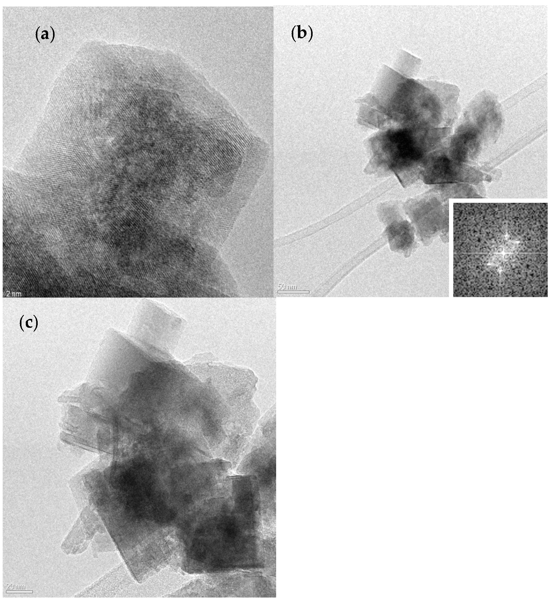
The results obtained after the investigation of the crystal structure and morphology of InN using HRTEM are shown in Figure 2. The powder was investigated after being supported onto Cu grids coated with a holey carbon film. The HRTEM images revealed that crystals synthesized at 93 °C for 3 h exhibited a cubic crystal shape, verifying the experimental findings obtained through XRD. As noticed, the crystal’s average width was approximately 30 nm, aligning closely with the XRD results calculated using the Scherrer equation (around 20 nm). Additionally, the crystal exhibited growth along the (101) axis, with a corresponding d value measured at 0.270 nm.
The XRD patterns of TiO2 decorated with InN nanoparticles and Kronos 1077 titania are shown in Figure 3, exhibiting the presence of the peaks which are characteristic of the anatase phase. These peaks appeared at 25.34°, 37.03°, 37.81°, 38.58°, 48.14°, 53.94°, 55.20°, 62.82° and 69°, and demonstrated, as expected, the absence of another crystallographic phase of TiO2, since commercial Kronos 1077 titania is 100% anatase [59]. Furthermore, the main purpose of sonochemical technique was the decoration of InN nanoparticles onto the surface of TiO2, without any further intervention in the crystal lattice of TiO2.
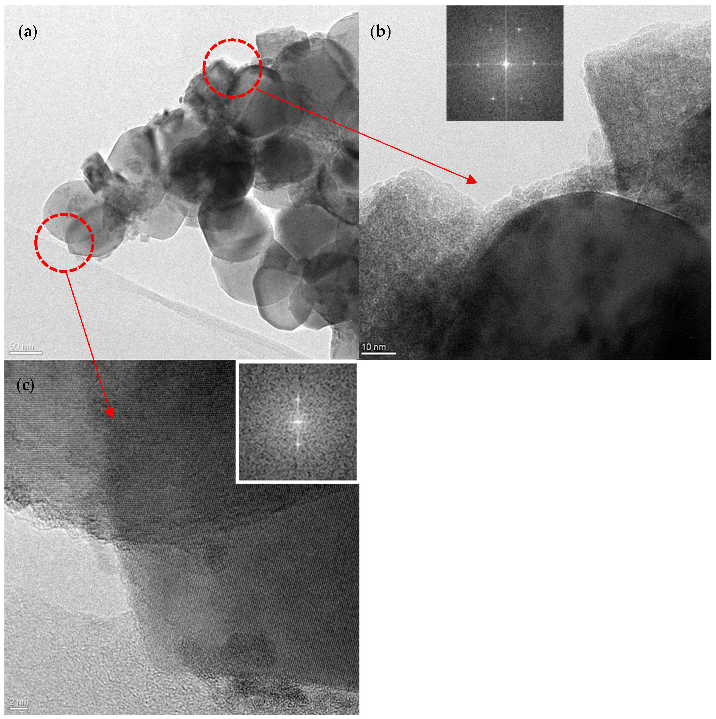
The HRTEM technique was used to investigate the crystal structure and morphology of TiO2 decorated with InN nanoparticles. HRTEM images of TiO2 decorated with InN nanoparticles are shown in Figure 4. The predominant morphological features that are distinctive of the Kronos system include the well-ordered TiO2 crystallites with almost unchanged average dimensions, in line with the XRD results. The TiO2 crystal plane, specifically the (101) family, exhibited a distance of d = 0.352 nm, which is characteristic for anatase (ICDD n. 21-1272). InN nanoparticles were spotted on top of the titania crystals with a low distribution, attributed to a decoration rate of 10% w/w. The (102) family planes demonstrated a distance of d = 0.208 nm. This result is in accordance with previous studies that found a distance value of 0.21 n.
3.2. Photocatalytic Tests
The photocatalytic properties of TiO2 decorated with InN nanoparticles was investigated through the photodegradation of MB as a test substance. The method used to assess the photocatalytic activity of TiO2 against MB, a natural dye, involved the observation of its colour changes. In the present study, the sample was exposed to ultraviolet irradiation and alterations in the colour were observed. Afterwards, the estimation of the degree of degradation was based on the reduction in the absorption at the maximum wavelength as follows
where Ao and Ai are the absorbance values of the dye solution before and after irradiation, respectively. In Figure 5, the absorbance spectrum versus the wavelength for MB, with TiO2 as a photocatalyst, is shown at different time intervals. The absorbance spectrum indicated that the maximum absorbance occurred at a wavelength of 663–664 nm. Zero time to corresponded to the initial absorbance spectrum before UV irradiation and after the addition of TiO2 where the peak reached its highest value Ao = 1536. As the illumination started, the absorbance spectra were recorded at different time intervals, showing a reduction in the peak values. This indicated a decrease in the absorbance values during the experiment. After 100 min of exposure to UV light, the absorbance peak became nearly smooth, reaching its lowest value (Ai = 914), while the blue colour of the solution became colourless. The degree of decolouration was calculated to be 40.5%.
Figure 6 shows the absorbance spectrum versus wavelength for MB at different time intervals, using the TiO2 decorated with InN nanoparticles as a photocatalyst. According to the obtained measurements, the maximum absorbance occurred at a wavelength of 664 nm. The zero time to corresponded to the initial absorbance spectrum before UV irradiation and after TiO2, with the peak reaching the highest value (Ao = 1035). After the illumination started, the absorbance spectrum was recorded at different time intervals, revealing a reduction in the peak values. This indicated that the absorbance value decreased with an increase in the exposure time. After 130 min of exposure to UV light, the absorbance peak became nearly smooth, reaching the lowest value (Ai = 398). Moreover, the blue colour of the solution became colourless. The degree of degradation was calculated to be 61.5%. The determination of the degree of decolouration using different photocatalysts revealed a 41.8% increase in the decolouration of MB diluted in an aqueous solution by applying TiO2 decorated with InN nanoparticles as a photocatalyst.
The results of all experiments are compiled in Figure 7. It is obvious that InN itself was not photoactive and did not contribute to the decolouration of MB. On the contrary, its combination with TiO2 led to an effective photocatalyst which outperformed pure Kronos® Titania by 41.8% and achieved 95% decolouration after 130 min.
In order to assess the reducing power of photoexcited electrons, one can examine the energy level at the lower edge of the conduction band in a semiconductor. The upper edge of the valence band provides an indication of the oxidation strength of the holes. Doping semiconductors contributes to the lifetime extension of charge carriers, especially when the energy levels of the dopants are below the conduction band or above the valence band of TiO2. Moreover, if the electronic coupling effect between the dopant and the semiconductor is strong enough to change the band’s structure, band gap narrowing can also become possible. While band gap narrowing may lead to a modest decrease in the photo-redox potential energy of TiO2, the increased efficiency of photo-absorption or the accelerated generation rate of change carriers can compensate for this adverse impact. This negative effect significantly enhances the overall photo-reactivity, particularly when the redox potential of H2O/•OH coupling (approximately −2.8 V) falls within the band gap [60].
To enhance charge separation on the surface of a semiconductor, one effective approach is a connection with another semiconductor, as in the case of TiO2 decorated with InN. The presence of two semiconductors facilitates the injection of electrons into the lowest conduction band of the second semiconductor, which, in this case, was TiO2.
The charge separation mechanism in a coupled semiconductor system involves the injection of photo-generated electrons in InN into the lower conduction band of TiO2. Regarding the processes of interfacial charge transfer in coupled semiconductor systems, the two particles were in direct contact with each other. Additionally, both holes and electrons were accessible on the surface for selective oxidation and reduction processes [61].
4. Conclusions
This article presents an alternative and much more rapid synthesis technique for InN. Despite the challenges associated with the synthesis of InN, the production of InN nanoparticles with an average size of 20 nm was achieved using ultrasound for 3 h. HRTEM images of the crystals revealed a cubic shape, aligning with the experimental evidence obtained through XRD. In particular, the use of ultrasound for the preparation of InN resulted in smaller-sized nanoparticles compared with other methods.
Furthermore, the use of ultrasound allowed the surface decoration of micrometric titania. After the successful decoration of the InN nanoparticles onto TiO2, the potential effects of the photocatalytic activity of TiO2 were investigated. While TiO2 is a highly effective material in photocatalysis, its efficiency is limited under visible light. The obtained results showed that under UV irradiation, InN nanoparticles strongly improved the photocatalytic activity of TiO2.
Author Contributions
Conceptualization, C.A. and G.S.; methodology, A.P. and C.A.; validation, C.A. and G.S.; formal analysis, A.P.; investigation, A.P.; resources, G.S. and C.A.; writing—original draft preparation, C.A. and A.P.; writing—review and editing, C.A. and P.P.; visualization, C.A., G.S., A.P. and P.P.; project administration, G.S. and P.P.; funding acquisition, G.S. and C.A. All authors have read and agreed to the published version of the manuscript.
Funding
This research received no external funding.
Institutional Review Board Statement
Not applicable.
Informed Consent Statement
Not applicable.
Data Availability Statement
Data are available from the authors upon request.
Acknowledgments
We are indebted to G. Cerrato, Uni. Torino, Italy for the TEM micrographs.
Conflicts of Interest
The authors declare no conflicts of interest.
References
- Wang, S.; Tian, H.; Luo, Y.; Yu, J.; Ren, C.; Sun, C.; Xu, Y.; Sun, M. First-principles calculations of aluminium nitride monolayer with chemical functionalization. Appl. Surf. Sci. 2019, 481, 1549–1553. [Google Scholar] [CrossRef]
- Bhuiyan, A.G.; Hashimoto, A.; Yamamoto, A. Indium nitride (InN): A review on growth, characterization, and properties. J. Appl. Phys. 2003, 94, 2779. [Google Scholar] [CrossRef]
- Polyakov, V.M.; Schwierz, F. Low-field electron mobility in wurtzite InN. Appl. Phys. Lett. 2006, 88, 032101. [Google Scholar] [CrossRef]
- Takai, S.; Lu, Y.; Oda, O.; Takeda, K.; Kondo, H.; Ishikawa, K.; Sekine, M.; Hori, M. Growth of InN films by radical-enhanced metal organic chemical vapor deposition at a low temperature of 200 °C. Jpn. J. Appl. Phys. 2017, 56, 06HE08. [Google Scholar] [CrossRef]
- Davydov, V.Y.; Klochikhin, A.A.; Seisyan, R.P.; Emtsev, V.V.; Ivanov, S.V.; Bechstedt, F.; Furthmuller, J.; Harima, H.; Mudrui, A.V.; Aderhold, J.; et al. Absorption and Emission of Hexagonal InN. Evidence of Narrow Fundamental Band Gap. Phys. Status Solidi (B) 2002, 229, R1–R3. [Google Scholar] [CrossRef]
- Wu, J.; Walukiewicz, W.; Yu, K.M.; Ager, J.W.; Haller, E.E. Unusual properties of the fundamental band gap of InN. Appl. Phys. Lett. 2002, 80, 3697. [Google Scholar] [CrossRef]
- Hori, M.; Kano, V.; Yamaguchi, T.; Saito, Y.; Araki, T.; Nanishi, Y.; Teraguchi, N.; Suzuki, A. Optical Proper-ties of InxGa1−xN with Entire Alloy Composition on InN Buffer Layer Grown by RF-MBE. Phys. Status Solidi (B) 2002, 234, 750–754. [Google Scholar] [CrossRef]
- Tansley, T.L.; Foley, C.P. Optical band gap of indium nitride. J. Appl. Phys. 1986, 59, 3241–3244. [Google Scholar] [CrossRef]
- Guo, Q.; Yoshida, A. Temperature Dependence of Band Gap Change in InN and AlN. Jpn. J. Appl. Phys. 1994, 33, 2453–2456. [Google Scholar] [CrossRef]
- Wu, J.; Walukiewicz, W.; Shan, W.; Yu, K.M.; Ager, J.W.; Li, S.X.; Haller, E.E.; Lu, H.; Schaff, W.J. Temperature dependence of the fundamental band gap of InN. J. Appl. Phys. 2003, 94, 4457. [Google Scholar] [CrossRef]
- Wu, J. When group-III nitrides go infrared: New properties and perspectives. J. Appl. Phys. 2009, 106, 011101. [Google Scholar] [CrossRef]
- Degheidy, A.; Elkenany, E. Electronic, optical, and mechanical properties of BN, AlN, and InN with zinc-blende structure under pressure. Chin. Phys. B 2017, 26, 086103. [Google Scholar] [CrossRef]
- Ahmad, U.; Aslam, S.; Mustafa, F.; Jamil, A.; Ashfaq Ahmad, M. Synthesis and characterization of InN quantum dots for optoelectronic applications. Opt. Int. J. Light Electron Opt. 2018, 173, 97–100. [Google Scholar] [CrossRef]
- Bai, Y.J.; Liu, Z.G.; Xu, X.G.; Cui, D.L.; Hao, X.P.; Feng, X.; Wang, Q.L. Preparation of InN nanocrystals by solvo-thermal method. J. Cryst. Growth 2002, 241, 189–192. [Google Scholar] [CrossRef]
- Yamamoto, A.; Tsujino, M.; Ohkubo, M.; Hashimoto, A. Metalorganic chemical vapor deposition growth of InN for InN/Si tandem solar cell. Sol. Energy Mater. Sol. Cells 1994, 35, 53. [Google Scholar] [CrossRef]
- Chen, Y. A Solution-Liquid-Solid Approach to Colloidal Indium Nitride Nanoparticles from Simple Alkylamide Precursors and Investigation of Its Mechanism. Master’s Thesis, Michigan State University, East Lansing, MI, USA, 2017. [Google Scholar] [CrossRef]
- Kasap, S.; Capper, P. (Eds.) Springer Handbook of Electronic and Photonic Materials; Springer Science &Business Media: New York, NY, USA, 2007; ISBN-13: 978-0-387-26059-4. [Google Scholar]
- Krames, M.R. Status and Future of High-Power Light-Emitting Diodes for Solid-State Lighting. J. Disp. Technol. 2007, 3, 160. [Google Scholar] [CrossRef]
- Nie, C.; Zhang, R.; Xie, Z.-L.; Xiu, X.-Q.; Liu, B.; Fu, D.-Y.; Liu, Q.-J.; Han, P.; Gu, S.-L.; Shi, Y.; et al. Synthesis of [100] Wurtzite InN Nanowires and [011] Zinc-Blende InN Nanorods. Chin. Phys. Lett. 2008, 25, 1780–1783. [Google Scholar] [CrossRef]
- Bhuiyan, A.G.; Yamamoto, A.; Hashimoto, A.; Ito, Y. High temperature growth of InN on GaP(1 1 1)B substrate using a new two-step growth method. J. Cryst. Growth 2002, 236, 59–65. [Google Scholar] [CrossRef]
- Yang, C.; Wang, X.; Xiao, H.; Zhang, X.; Hu, G.; Ran, J.; Wang, C.; Li, J.; Li, J.; Wang, Z. Growth temperature dependences of InN films grown by MOCVD. Appl. Surf. Sci. 2008, 255, 3149. [Google Scholar] [CrossRef]
- Chen, W.C.; Kuo, S.; Lai, F.; Lin, W.; Hsiao, C.; Tsai, D.P. Indium nitride epilayer prepared by UHV-plasma-assisted metalorganic molecule beam epitaxy. J. Vac. Sci. Technol. B 2011, 29, 051204. [Google Scholar] [CrossRef]
- Fu, S.P.; Lin, T.J.; Su, W.S.; Shieh, C.Y.; Chen, Y.F.; Chang, C.A.; Chen, N.C.; Chang, P.H. Influence of hydrogenation on surface morphologies, transport, and optical properties of InN epifilms. J. Appl. Phys. 2006, 99, 126102. [Google Scholar] [CrossRef]
- Fujiwara, K.; Ishii, A.; Ohta, J.; Fujioka, H.; Oshima, M. Experimental and theoretical investigation on the structural properties of InN grown on sapphire. Thin Solid Films 2004, 112, 464–465. [Google Scholar] [CrossRef]
- Nakamura, S.; Harada, Y.; Seno, M. Novel metalorganic chemical vapor deposition system for GaN growth. Appl. Phys. Lett. 1991, 58, 2021. [Google Scholar] [CrossRef]
- Kubota, K.; Kobayashi, Y.; Fujimoto, K. Preparation and properties of III–V nitride thin films. J. Appl. Phys. 1989, 66, 2984. [Google Scholar] [CrossRef]
- Ilhom, S.; Mohammad, A.; Shukla, D.; Grasso, J.; Willis, B.; Okyay, A.; Biyikli, N. Elucidating the role of nitrogen plasma composition in the low-temperature self-limiting growth of indium nitride thin films. RSC Adv. 2020, 10, 27357–27368. [Google Scholar] [CrossRef]
- Johnson, M.C.; Lee, C.J.; Bourret-Courchesne, E.D.; Konsek, S.L.; Aloni, S. Growth and morphology of 0.80eV photoemitting indium nitride nanowires. Appl. Phys. Lett. 2004, 85, 5670. [Google Scholar] [CrossRef]
- Hsieh, J.C.; Yun, D.S.; Hu, E.; Belcher, A.M. Ambient pressure, low-temperature synthesis and characterization of colloidal InN nanocrystals. J. Mater. Chem. 2010, 20, 1435–1437. [Google Scholar] [CrossRef] [PubMed]
- Chao, C.; Chang, H.; Hsu, T.; Hsiao, C.; Kei, C.; Kuo, S.; Chyi, J. Optical properties of indium nitride nanorods prepared by chemical-beam epitaxy. Nanotechnology 2006, 17, 3930–3932. [Google Scholar] [CrossRef]
- Khashan, K.S.; Taha, J.M.; Abbas, S.F. Fabrication and Properties of InN NPs/Si as a photodetector. Energy Procedia 2017, 119, 656–661. [Google Scholar] [CrossRef]
- Chirico, P.; Hector, A.L. Solvothermal Synthesis of Gallium and Indium Nitrides Using Lithium Amide. Z. Naturforschung B 2010, 65, 1051–1057. [Google Scholar] [CrossRef]
- Li, B.; Xie, Y.; Huang, J.; Liu, Y.; Qian, Y. A novel method for the preparation of III-V semiconductors: Sonochemical synthesis of InP nanocrystalls. Ultrason. Sonochem. 2001, 8, 331–334. [Google Scholar] [CrossRef]
- Gedanken, A. Using sonochemistry for the fabrication of nanomaterials. Ultrason. Sonochem. 2004, 11, 47–55. [Google Scholar] [CrossRef]
- Gedanken, A. Using Sonochemical Methods for the Preparation of Mesoporous Materials and for the Deposition of Catalysts into the Mesopores. Chem. Eur. J. 2001, 7, 4546–4552. [Google Scholar] [CrossRef]
- Livage, J. Amorphous transition metal oxides. J. Phys. Colloq. 1981, 42, C4–C981. [Google Scholar] [CrossRef]
- Landau, M.V.; Vradman, L.; Herskowitz, M.; Koltypin, Y.; Gedanken, A. Ultrasonically Controlled Deposition–Precipitation. J. Catal. 2001, 201, 22–36. [Google Scholar] [CrossRef]
- Perkas, N.; Wang, Y.; Koltypin, Y.; Gedanken, A.; Chandrasekaran, S. Mesoporous iron–titania catalyst for cyclohexane oxidation. Chem. Commun. 2001, 11, 988–989. [Google Scholar] [CrossRef]
- Ramesh, S.; Koltypin, Y.; Prozorov, R.; Gedanken, A. Sonochemical Deposition and Characterization of Nanophasic Amorphous Nickel on Silica Microspheres. Chem. Mater. 1997, 9, 546. [Google Scholar] [CrossRef]
- Stucchi, M.; Bianchi, C.L.; Pirola, C.; Vitali, S.; Cerrato, G.; Morandi, S.; Argirusis, C.; Sourkouni, G.; Sakkas, P.M.; Capucci, V. Surface decoration of commercial micro-sized TiO2 by means of high energy ultrasound: A way to enhance its photocatalytic activity under visible light. Appl. Catal. B Environ. 2015, 178, 124–132. [Google Scholar] [CrossRef]
- Stucchi, M.; Bianchi, C.L.; Argirusis, C.; Pifferi, V.; Cerrato, G.; Boffito, D.C. Ultrasound assisted synthesis of Ag-decorated TiO2 active in visible light. Ultrason. Sonochem. 2018, 40, 282–288. [Google Scholar] [CrossRef]
- Xie, Y.; Ali, G.; Yoo, S.H.; Cho, S.O. Sonication-Assisted Synthesis of CdS Quantum-Dot-Sensitized TiO2 Nanotube Arrays with Enhanced Photoelectrochemical and Photocatalytic Activity. ACS Appl. Mater. Interfaces 2010, 2, 2910–2914. [Google Scholar] [CrossRef]
- Fujishima, A.; Honda, K. Electrochemical evidence for the mechanism of the primary stage of photosynthesis Bull. Chem. Soc. Jpn. 1971, 44, 1148. [Google Scholar] [CrossRef]
- Fujishima, A.; Honda, K. Electrochemical Photolysis of Water at a Semiconductor Electrode. Nature 1972, 238, 37. [Google Scholar] [CrossRef] [PubMed]
- Matthews, R.W.; McEvoy, S.R. Photocatalytic degradation of phenol in the presence of near-UV illuminated titanium dioxide. J. Photochem. Photobiol. A Chem. 1992, 64, 231. [Google Scholar] [CrossRef]
- Muruganandham, M.; Swaminathan, M. Photocatalytic decolourisation and degradation of Reactive Orange 4 by TiO2-UV process. Dye. Pigment. 2006, 68, 133. [Google Scholar] [CrossRef]
- Alberci, R.M.; Jardim, W.F. Photocatalytic destruction of VOCs in the gas-phase using titanium dioxide. Appl. Catal. B Environ. 1997, 14, 55. [Google Scholar] [CrossRef]
- Zhu, X.; Xu, H.; Bi, C.; Song, H.; Zhou, G.; Zhong, K.; Yang, J.; Yi, J.; Xu, H.; Wang, X. Piezo-photocatalysis for efficient charge separation to promote CO2 photoreduction in nanoclusters. Ultrason. Sonochem. 2023, 101, 106653. [Google Scholar] [CrossRef] [PubMed]
- Arora, I.; Chawla, H.; Chandra, A.; Sagadevan, S.; Garg, S. Advances in the strategies for enhancing the photocatalytic activity of TiO2: Conversion from UV-light active to visible-light active photocatalyst. Inorg. Chem. Commun. 2022, 143, 109700. [Google Scholar] [CrossRef]
- Anandan, S.; Ikuma, Y.; Niwa, K. An Overview of Semi-Conductor Photocatalysis: Modification of TiO2 Nanomaterials. Solid State Phenom. 2010, 162, 239–260. [Google Scholar] [CrossRef]
- Koczkur, K.M.; Mourdikoudis, S.; Polavarapu, L.; Skrabalak, S.E. Polyvinylpyrrolidone (PVP) in nanoparticle synthesis. Dalton Trans. 2015, 44, 17883–17905. [Google Scholar] [CrossRef] [PubMed]
- Obata, H.; Koizumi, M. Photochemical Reactions between Methylene Blue and Tri-, Di- and Monomethylamine. I. Bull. Chem. Soc. Jpn. 1957, 30, 136–142. [Google Scholar] [CrossRef]
- Obata, H.; Kogasaka, K.; Koizumi, M. Photochemical Reactions between Methylene Blue and Tri-, Di- and Monomethylamine. III. The Behavior of Methylene Blue in the Presence of Oxygen. Bull. Chem. Soc. Jpn. 1959, 32, 125. [Google Scholar] [CrossRef]
- Usui, Y.; Obata, H.; Koizumi, M. Photoreduction of methylene blue by visible light in the aqueous solution containing certain kinds of inorganic salts. I. General features of the reaction. Bull. Chem. Soc. Jpn. 1961, 34, 1049–1056. [Google Scholar] [CrossRef]
- Tichapondwa, S.M.; Newman, J.P.; Kubheka, O. Effect of TiO2 phase on the photocatalytic degradation of methylene blue dye. Phys. Chem. Earth Parts A/B/C 2020, 118–119, 102900. [Google Scholar] [CrossRef]
- Mills, A.; Wang, J. Photobleaching of methylene blue sensitised by TiO2: An ambiguous system? J. Photochem. Photobiol. A Chem. 1999, 127, 123–134. [Google Scholar] [CrossRef]
- Houas, A.; Lachheb, H.; Ksibi, M.; Elaloui, E.; Guillard, C.; Herrmann, J.-M. Photocatalytic degradation pathway of methylene blue in water. Appl. Catal. B Environ. 2001, 31, 145. [Google Scholar] [CrossRef]
- Gu, S.; Fu, B.; Dodbiba, G.; Fujita, T.; Fang, B. A sustainable approach to separate and recover indium and tin from spent indium–tin oxide targets. RSC Adv. 2017, 7, 52017. [Google Scholar] [CrossRef]
- Stucchi, M.; Bianchi, C.L.; Pirola, C.; Cerrato, G.; Morandi, S.; Argirusis, C.; Capucci, V. Copper NPs decorated titania: A novel synthesis by high energy US with a study of the photocatalytic activity under visible light. Ultrason. Sonochem. 2016, 31, 295–301. [Google Scholar] [CrossRef]
- Fujii, M.; Kawai, T.; Kawai, S. Photocatalytic activity and the energy levels of electrons in a semiconductor particle under irradiation. Chem. Phys. Lett. 1984, 106, 83–98. [Google Scholar] [CrossRef]
- Bedja, I.; Kamat, P.V. Capped Semiconductor Colloids. Synthesis and Photoelectrochemical Behavior of TiO2-Capped SnO2 Nanocrystallites. J. Phys. Chem. 1995, 99, 9182–9188. [Google Scholar] [CrossRef]
Figure 1.
(a) XRD pattern of InN nanoparticles produced by the sonochemical method. (b) Typical XRD pattern of InN nanoparticles according to Bai et al. [14].
Figure 1.
(a) XRD pattern of InN nanoparticles produced by the sonochemical method. (b) Typical XRD pattern of InN nanoparticles according to Bai et al. [14].
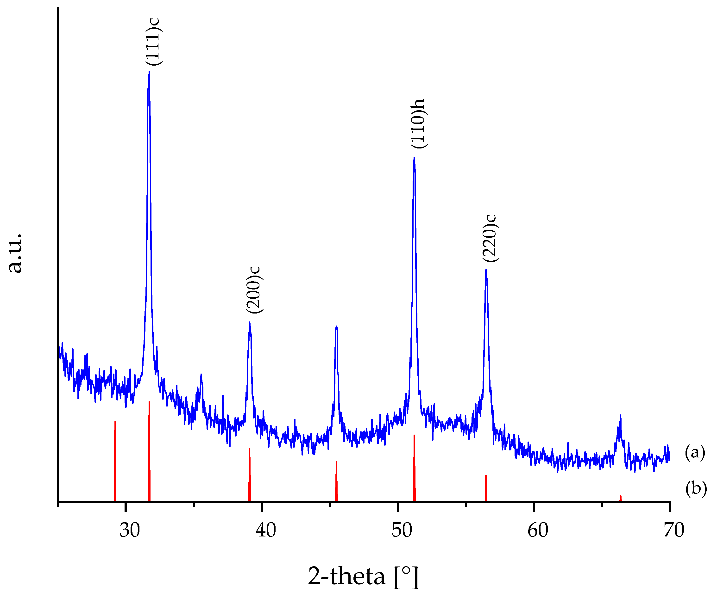
Figure 2.
HRTEM images of InN nanoparticles: (a) 2 nm scale bar; (b) 50 nm scale bar; (c) 20 nm scale bar.
Figure 2.
HRTEM images of InN nanoparticles: (a) 2 nm scale bar; (b) 50 nm scale bar; (c) 20 nm scale bar.

Figure 3.
XRD pattern of KRONOS® TiO2 [59] decorated with InN nanoparticles.
Figure 3.
XRD pattern of KRONOS® TiO2 [59] decorated with InN nanoparticles.
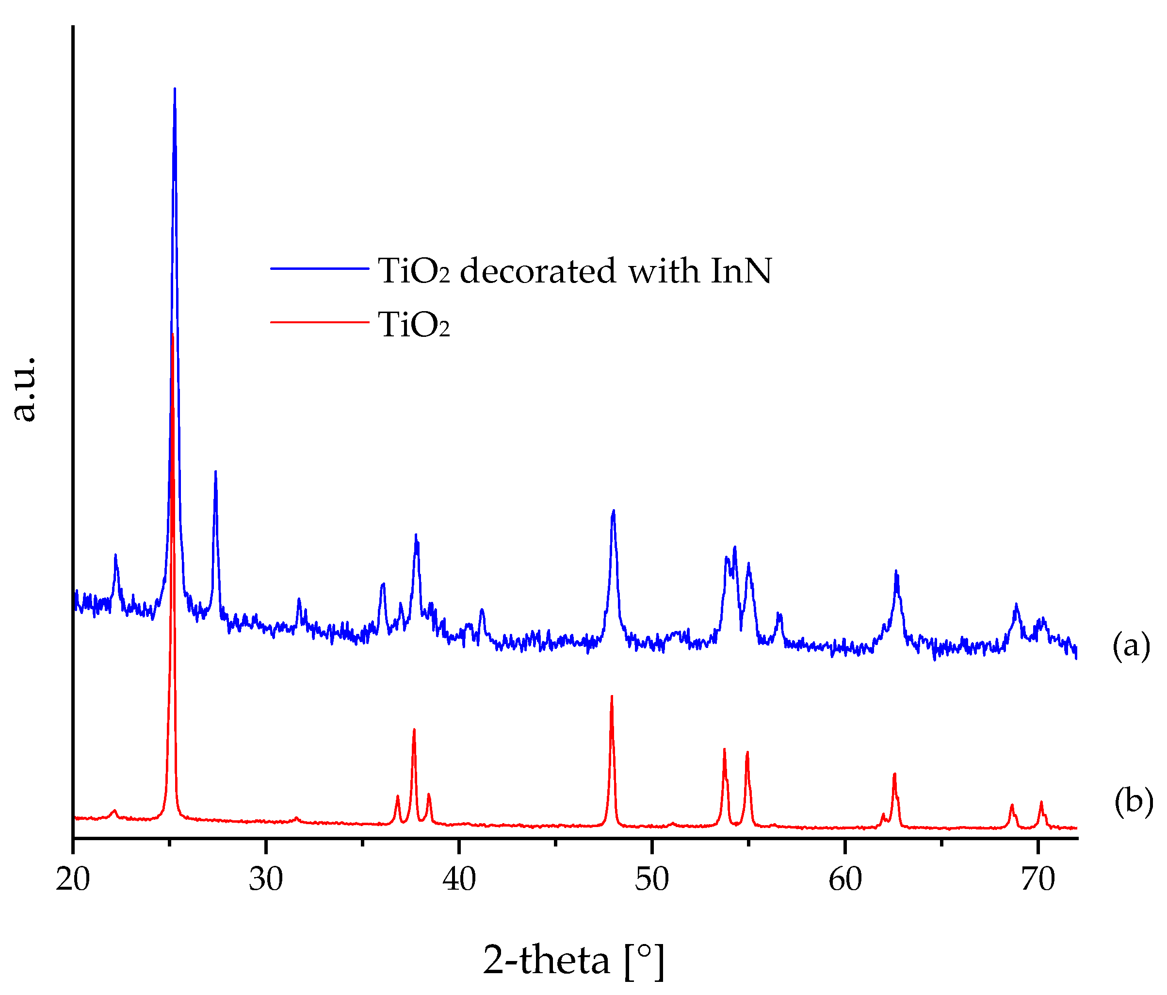
Figure 4.
HRTEM images showing the decoration of TiO2 with InN nanoparticles: (a) low magnification; (b) (101) TiO2; (c) (102) InN.
Figure 4.
HRTEM images showing the decoration of TiO2 with InN nanoparticles: (a) low magnification; (b) (101) TiO2; (c) (102) InN.

Figure 5.
Absorbance spectrum of MB using TiO2 Kronos 1077 as a photocatalyst.

Figure 6.
Absorbance spectra of MB using TiO2 decorated with InN nanoparticles, proving its activity as a photocatalyst.
Figure 6.
Absorbance spectra of MB using TiO2 decorated with InN nanoparticles, proving its activity as a photocatalyst.
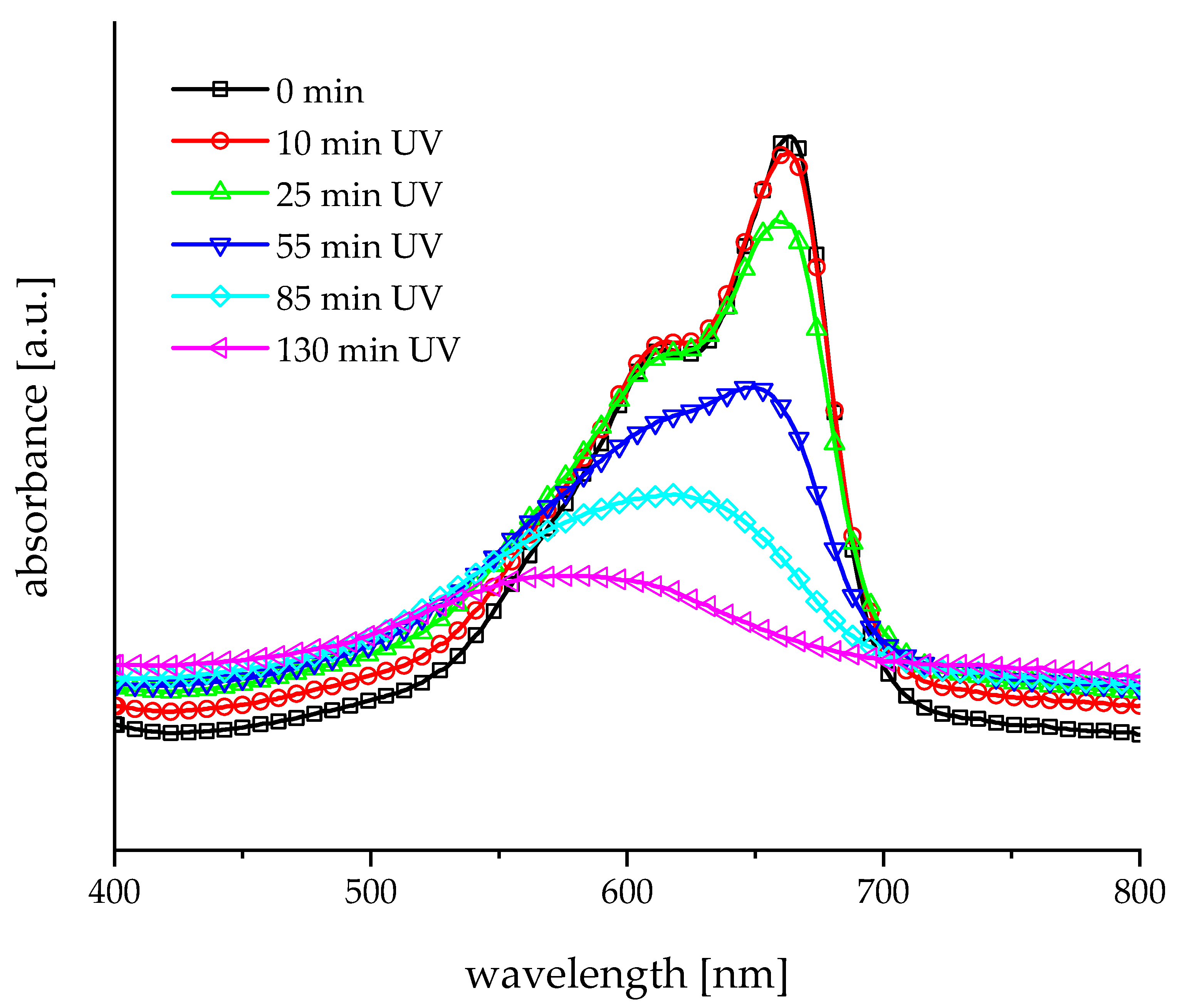
Figure 7.
Development of the decolouration over time using different materials in this study.

Disclaimer/Publisher’s Note: The statements, opinions and data contained in all publications are solely those of the individual author(s) and contributor(s) and not of MDPI and/or the editor(s). MDPI and/or the editor(s) disclaim responsibility for any injury to people or property resulting from any ideas, methods, instructions or products referred to in the content. |
© 2024 by the authors. Licensee MDPI, Basel, Switzerland. This article is an open access article distributed under the terms and conditions of the Creative Commons Attribution (CC BY) license (https://creativecommons.org/licenses/by/4.0/).
Share and Cite
MDPI and ACS Style
Paraskevopoulou, A.; Pandis, P.; Argirusis, C.; Sourkouni, G. Sonochemical Synthesis of Indium Nitride Nanoparticles and Photocatalytic Composites with Titania. Ceramics 2024, 7, 478-490. https://doi.org/10.3390/ceramics7020031
AMA Style
Paraskevopoulou A, Pandis P, Argirusis C, Sourkouni G. Sonochemical Synthesis of Indium Nitride Nanoparticles and Photocatalytic Composites with Titania. Ceramics. 2024; 7(2):478-490. https://doi.org/10.3390/ceramics7020031
Chicago/Turabian StyleParaskevopoulou, Aikaterina, Pavlos Pandis, Christos Argirusis, and Georgia Sourkouni. 2024. "Sonochemical Synthesis of Indium Nitride Nanoparticles and Photocatalytic Composites with Titania" Ceramics 7, no. 2: 478-490. https://doi.org/10.3390/ceramics7020031