Simulation of an S-Band MILO with Adjustable Beam Dump


Center for Pulsed Power and Power Electronics, Texas Tech University, Lubbock, TX 79409-3102, USA
*
Author to whom correspondence should be addressed.
Plasma 2019, 2(2), 138-155; https://doi.org/10.3390/plasma2020011
Submission received: 11 March 2019
/
Revised: 16 April 2019
/
Accepted: 17 April 2019
/
Published: 3 May 2019
(This article belongs to the Special Issue High-Power Microwave and Plasma Interactions)
Abstract
:This paper details the design, simulation, and optimization of a low-impedance high repetition rate magnetically insulated transmission line oscillator (MILO) driven by a compact Marx generator. The project goals require the MILO to generate an radio frequency (RF) pulse within the S-band frequency range with a peak output power greater than 1 GW with greater than 10% efficiency. Its design is based on a set of base equation which provide critical component dimensions applied to a three-dimensional model constructed within CST studio suite used in a particle-in-cell (PIC) simulation. Additional to the geometric model, simulation of the MILO with non-ideal material properties and a lumped element modeling of the Marx generator were performed. The results of these simulations then informed changes to the model as to the optimizing performance of the device. Within the framework of the model, the final MILO design achieves the design goals with an approximate RF peak power of 4.5 GW at 2.5 GHz operating in the TM mode when an input driving pulse with a peak voltage of 600 kV while providing 58 kA is applied.
1. Introduction
High power microwave (HPM) sources continue to be a strong area of research for multiple applications. HPM sources have been employed for multiple military applications including electronic warfare or directed energy weapon systems [1]. Additionally, research within the field of plasma science employs HPM sources as a source for plasma experimentation [2]. This has led to research focused upon improvements in peak output power, power efficiency, repetition rate, and device lifetime with sources which do not require an externally applied electromagnetic field.
HPM sources like the magnetically insulated transmission line oscillator (MILO) are able to supply gigawatt power cross-field radio frequency (RF) output for such applications [1]. The construction is a coaxial design containing a resonant cavity which interacts with an electron beam to generate a high power microwave output pulse tuned to a specified frequency. During operation it generates electrical current strong enough to produce a self-insulating magnetic field and thus does not require an externally applied magnetic field for beam guidance. This makes the MILO a strong candidate for a practical, modern HPM source.
The study of the MILO as an HPM source starts with research performed by the Mendel research group in the late 1970s and early 1980s [3]. In addition to experimental studies, computer simulations are a critical tool in the development of HPM sources such as the MILO. These simulations are typically particle-in-cell (PIC) simulations that account for the particle interactions with the electromagnetic fields within the structure. Traditionally, software simulation packages such as KARAT and MAGIC have been employed in the modeling of MILO sources for research studies [3,4]. This study utilizes the CST Studio Suite (CST) set of simulation packages to study a three-dimensional modeled MILO while utilizing hardware acceleration techniques for GPU processing to reduce the overall runtime. The accelerated simulations allowed for the accounting of material properties, simulation with a lumped element defined excitation source, and parameter sweeping. These tools aided in the development of a MILO designed to deliver gigawatt peak RF power output with over 10% power efficiency operating in the S-band. The following is an account of the stages of developing a model to best achieve the design criteria.
2. Materials and Methods
The design of a MILO has been well documented by multiple authors. This paper follows a set of design equations as presented within a paper by G. Dixit et al. aiming to maximize the peak output power of a MILO operating within the L-band [3]. The equations take as an input the design frequency, cathode radius, and design criteria to calculate the approximate dimensions of the MILO device for maximized power output.
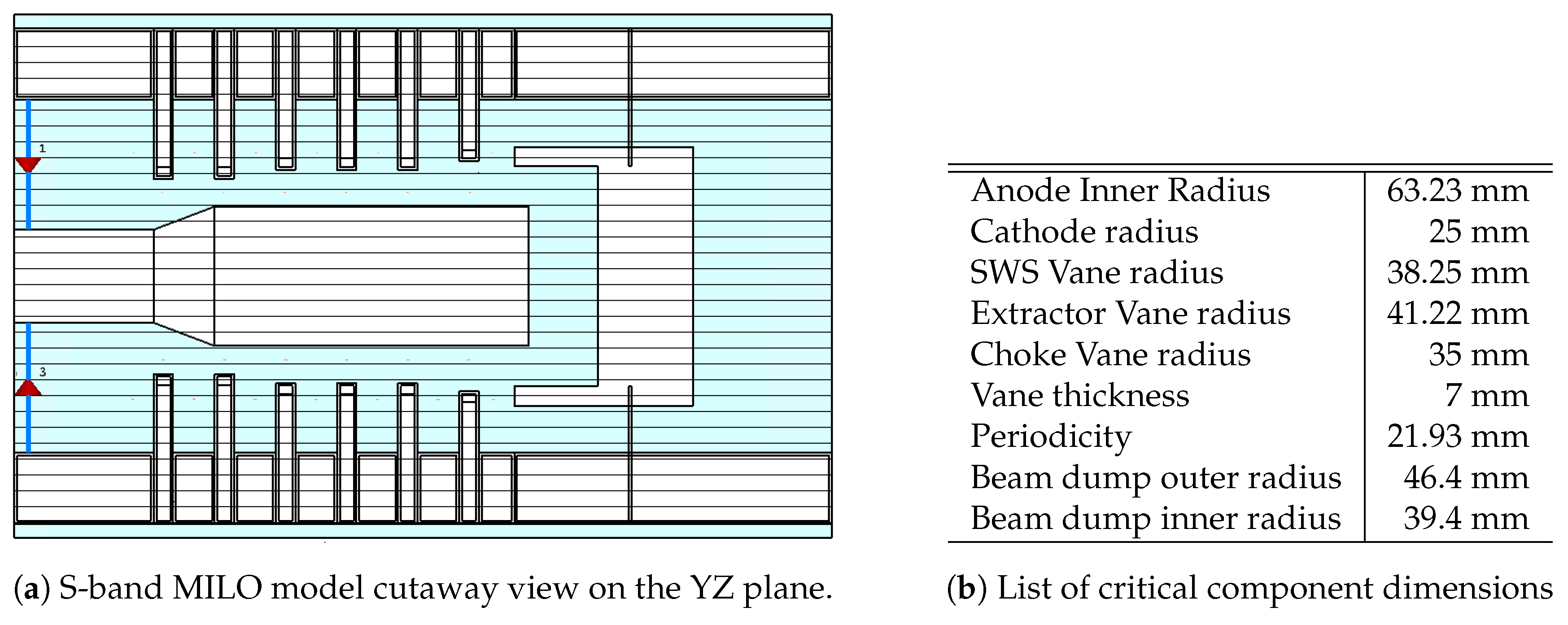
The equations that define the radius of the anode and vane structures within the MILO are listed within Table 1. Parameters such as the eigenvalue of the output mode (), speed of light (c), frequency (), cathode radius (), slow wave structure impedance (), and desired input impedance () define the vane structure to operate as desired [3].
Each of the following sections uses the same base set of equations to define the dimensions of the model detailed within that section. These models are then simulated within CST Studio Suite utilizing the Particle-in-Cell simulation provided by the software package. The results are then analyzed and used to inform the following stage of development of the simulation models. The following sections introduce additional simulation criteria, such as non-ideal material properties, lumped element source excitation, as well as parametric sweeps of MILO structural components, all with the purpose of optimizing the MILO performance. The simulations were accelerated using GPU acceleration within CST. The simulation machine has dual Xeon processors, 396 GB of RAM, and four Intel Tesla K80 with 32 GB of RAM available to each GPU.
2.1. L-Band MILO
The initial study focused on matching the results presented within the paper by Dixit from which the design equations originated. Fortunately, the paper provided not only the set of design equations but also a table with key component dimensions. The provided dimensions were then fed back through the equations to find the dimensions of all components of the MILO. The values in the table appear to have been adjusted from the original outputs of the design equations.
The simulation used only idealized materials, vacuum and a perfect electric conductor (PEC), with an applied voltage pulse fed through a set of four discrete ports at the input of the device spanning from the anode to cathode, simulation model and parameters shown in Figure 1. The pulse was an ideal trapezoidal pulse with a 30 ns rise time, 20 ns flat top, and 35 ns fall time, see Figure 2b. The output was captured through a waveguide port, a tool provided with CST capable of measuring a defined set of output modes. Post-processing was applied to the captured RF output to find the output frequency of the MILO by means of a Fourier transform.
2.2. S-Band MILO
The S-Band MILO was designed in the same manner as the L-Band MILO from the previous section. This includes the types of applied materials, excitation, signal recording, and boundary conditions of the simulation. However, additional components were added to the model to improve the convergence of the simulation results, model shown in Figure 3. The addition of a vacuum layer encasing the MILO before the boundary of the simulation and an improved definition of the MILO based on parametric techniques provided better control over the MILO’s structure without affecting the simulation results.
2.3. S-Band MILO with Materials
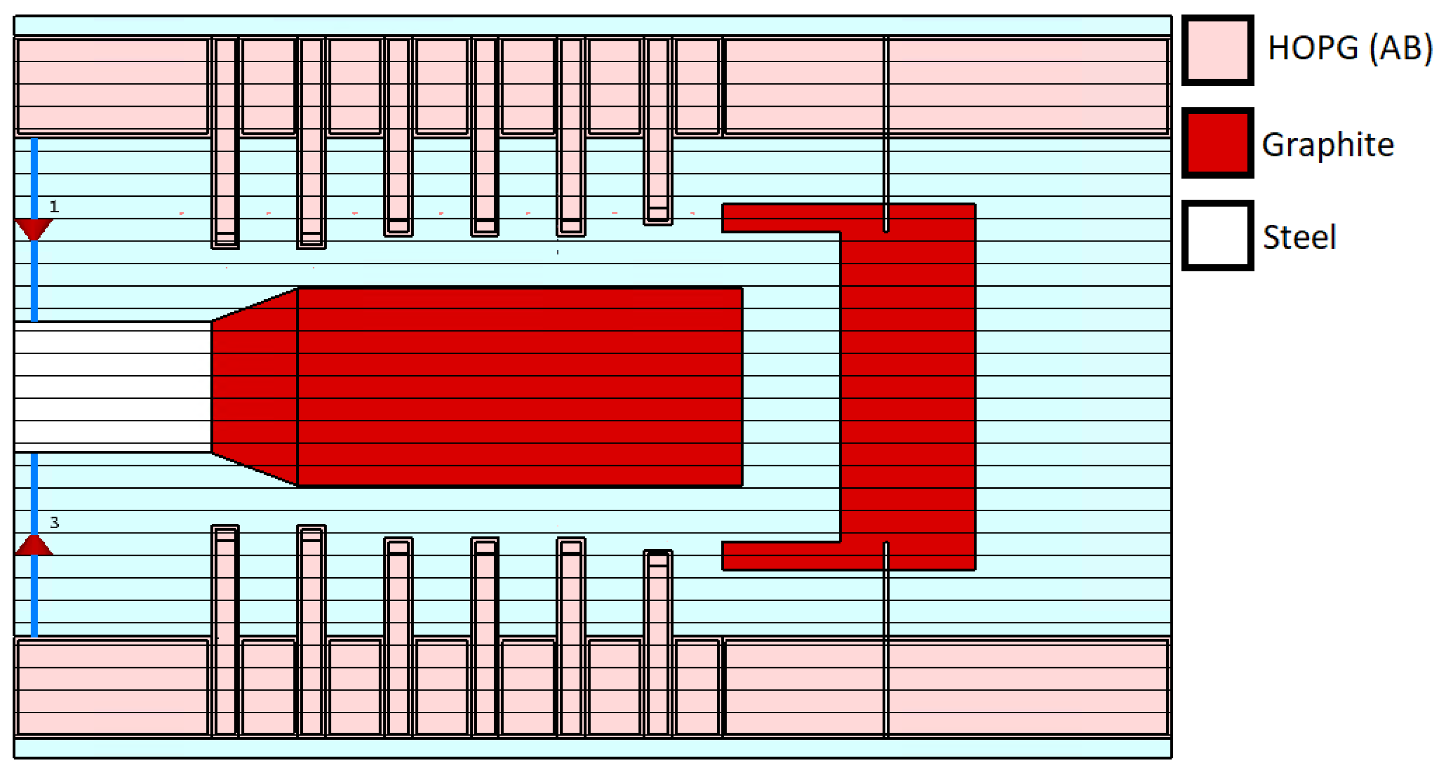
The desire to operate the MILO at a high repetition rate requires it to withstand intense heating during operation. Constructing the anode structure, including the slow wave structure (SWS), from highly ordered pyrolytic graphite (HOPG), a material with high thermal conductivity, enables the efficient transfer of heat during operation mitigating the negative effects of heat buildup such as material erosion. Accounting for the electrical properties of HOPG improved the accuracy of the simulation of the MILO. Within CST, a material property was assigned to a volume in three-dimensional space. The material property accounts for the electrical, mechanical, and thermal effects of the material during simulation. CST provided a material library containing a set of predefined materials, though for materials not included, a manual definition of the material may be provided through CST’s material dialog box. The location of the applied materials to the model are shown in Figure 4.
Materials fall into two broad categories within CST, normal and anisotropic. Anisotropic materials may have varying values of their electric, thermal, and mechanical properties depending upon orientation. CST did not contain a definition of the material properties for HOPG which had been decided for use of the SWS of the MILO. While able to define HOPG as anisotropic within CST, the required discretization of the simulation mesh to support such a large volume of anisotropic material with high electrical conductivity would require the number of mesh cells on the order of . The hardware available for simulation would not be able to preform such a task.
Instead the HOPG was defined as a lossy metal. A lossy metal is a material type within CST which accounts for factors such as skin depth through some preprocessing. This reduces the required mesh size for the simulation on the order of hundred of thousands, well within the capability of the available hardware. Unfortunately, lossy metals must be isotropic in definition. Assuming the surface currents which form on the fins of the SWS have the greatest impact upon device performance resulted in two simulation setups to evaluate the device performance with the applied material.
HOPG electrical properties, shown in Table 2, vary upon which axis the current is flowing within, having high electrical conductivity within the basal plane, AB plane, and low electric conductivity along the C-axis. As the material’s orientation may influence efficency, a pair of simulations were conducted to confirm which orientation of the HOPG is best. The simulations assumed the anode material was isotropic and had the electrical properties of either the AB plane or C-axis. It was assumed that by aligning the HOPG’s c-axis with the axis of symmetry for the MILO results in the better performance as the surface currents are met with the minimum resistance.
2.4. Marx Co-Simulation
Simulations which account for a realizable excitation source, such as a Marx generator, can be achieved through a process of co-simulation. This tool is available within CST by means of their schematic package, the setup shown in Figure 5. The co-simulation allows for a time-dependent simulation to be setup to run with the PIC simulation. These simulations were fed together such that activity of one is accounted for by the other. This allows a lumped element model of a Marx generator to feed the discrete port inputs of the MILO. The Marx generator used in the co-simulation will eventually be revised to match a physical equivalent, but for now the Marx was matched close to the input impedance of the MILO at approximately 12 Ohms.
2.5. Parameter Sweep
Finally, design optimization was performed by sweeping the value of key dimensions. The simulations were performed with ideal materials with the assumption this is a close approximation for HOPG constructed with the c-axis aligned with axis of symmetry of the MILO. These results were eventually merged together in order to maximize the performance of the final device. The anode return path ignored the impact of the HOPG c-axis electrical conductivity as the anode is constructed by a stack up of alternating materials. The gaps between vanes were constructed from stainless steel with connecting bolts providing a high conductivity return path for the current.
The simulation sweeps focused on four different parameters of the MILO model which will change as if the position of the beam dump was changed after the MILO is constructed. The parameters, shown in Figure 6, were the extractor gap, stub position, stub radius, and the overlap distance of the beam dump and the cathode.
3. Results
The following results are presented in the same order as the setups detailed in the previous section. Simulation results shown were focused on RF output power and frequency bandwidth.
3.1. L-Band MILO
3.2. S-Band MILO
Continuing to the S-Band MILO model defined in Figure 3b, the results show that average peak output power dropped from a maximum of 5 GW to approximately 4 GW, see Figure 8. The resultant frequency was far below the expected design frequency of 3 GHz, see Figure 9. A study by Fan et al. provides a set of equation which serve to modify the initial results [6]. These equations account for the losses within the LC resonant cavity which are ignored in the base design equations. The modified expected frequency was still higher than expected, but may be further accounted for by the properties of the RF Choke before the SWS and the extractor downstream of the SWS.
Since the excitation waveform was defined as ideal the measured current flowing through the discrete ports defined the MILO impedance. At peak operation, the MILO had an impedance of approximately 10 Ohms, drawing an average of 60 kA with 600 kV applied.
3.3. S-Band MILO with Materials
The inability to simulate the model with HOPG with anisotropic conductivity resulted in two different simulations to account for material orientation. The simulations assumed that the conductivity was isotropic and vary by selecting the conductivity in the basal plane or the c-axis. As the construction of the device will provide a return path along the outer shell through a material with a higher conductivity, such as stainless steel, this assumption will hold valid as the concern is the currents within the SWS.
3.3.1. Basal Plane (AB)
3.3.2. C-Axis
Contrary to the basal plane results, modeling the HOPG by its c-axis material properties causes a drastic impact on the performance of the modeled MILO, displayed in the plots of Figure 12 and Figure 13. The output power drops down to a peak output power of approximately 1 GW no longer operating within mode.
This results seem to agree with our assumption about the preferable orientation of the HOPG relative to surface current flow. Fortunately, as the basal plane is easily aligned as such and connects to return path through the anode shell, which is constructed from a metal with a high electric conductivity, to ground these result do not lead to much concern.
3.4. Marx Co-Simulation
The modeling of the MILO with a realizable excitation source, such as a Marx generator, provided valuable information about its potential performance. The MILO not only did not produce a RF output below the minimum voltage threshold, approximately 300 kV, but the oscillation during operation resulted in the MILO having a time dependent impedance [1]. Simulating the system where these parameters were variable during simulation provides valuable feedback about its expected operation.
The monitored input voltage at each of the discrete ports feeding the MILO had the expected oscillations as the impedance of the MILO varies in time, shown in Figure 14. The amplitude of these oscillations drastically increased as the MILO began to produce a RF signal. This directly related to the modulation in the current through the device.
Though the signal may differ, the peak output power, shown in Figure 15b, of the device was close to the same value measured with the ideal trapezoidal pulse from Figure 2b applied and the output frequency, show in Figure 16, stays about on target. As the requirements for running a co-simulation within CST were resource intensive this was advantageous as the idealized pulse may be used for an approximation of peak output power.
3.5. Parameter Sweep
The following were the results of the parameter sweeps performed over the extractor gap, stub location, stub radius, and cathode beam dump overlap. The simulations were performed with an idealized model with the idealized voltage pulse from Figure 2b applied. This lacked the addition realism that co-simulation and simulated material properties provide with the benefit of reduced runtime and an acceptable approximate answer.
3.5.1. Extractor Gap
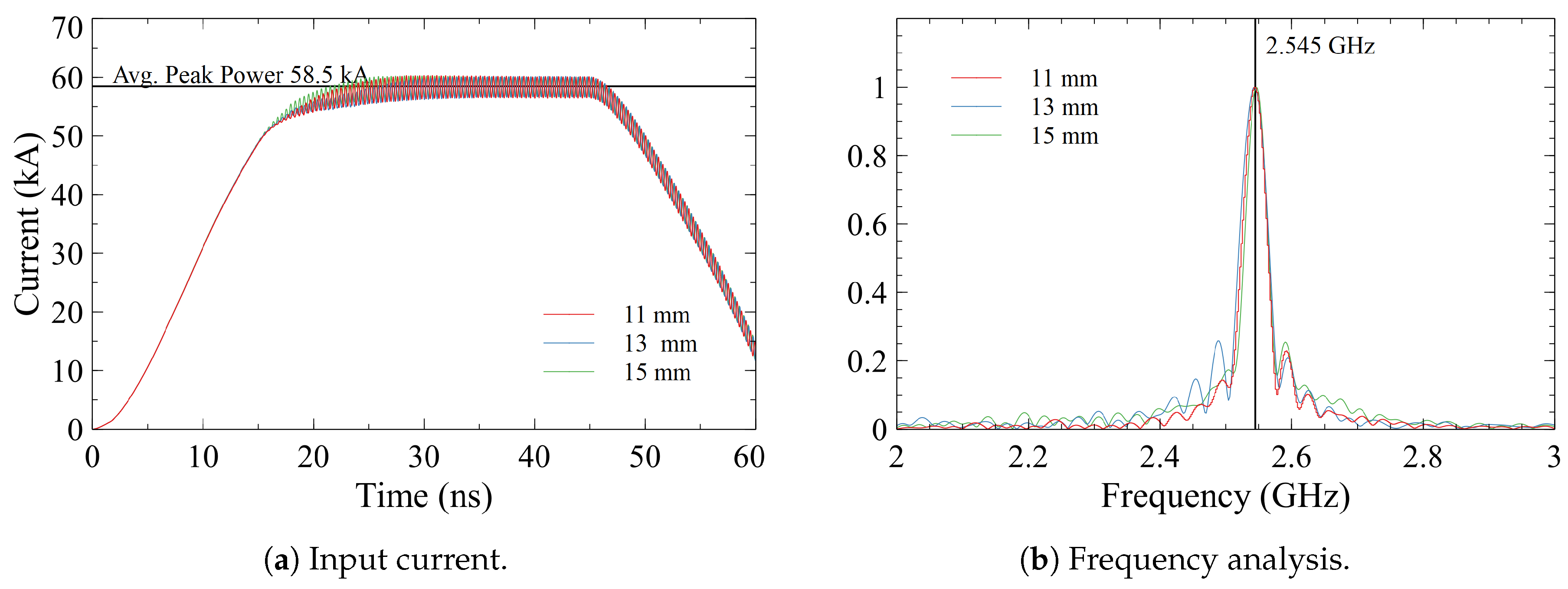
The base variation of the extractor gap distance did not show a great amount of impact on either the frequency or peak output power of the MILO device. The simulation of the extractor gap set at 11 mm took longer to achieve PI-mode operation which explains the delay to max output power seen in Figure 17a as there is mode competition. After PI-mode operation was achieved, the competing modes drop out and the peak power was approximately equal to the other simulated extractor gap distances. The input current and output frequency remained consistent throughout each simulation, shown in Figure 18.
3.5.2. Stub Radius
The output power does change slightly by varying the radius of the stubs that connects the beam dump to the anode, Figure 19. These variations of the peak output power are small however with minor differences in peak output RF power. A similar conclusion can be made about the frequency of the RF output, Figure 20.
3.5.3. Stub Location
The movement of the stub location had a noticeable impact upon the peak output power and frequency response of the MILO, shown in Figure 21 and Figure 22. This was related to matching the output frequency of the RF signal at a quarter-wavelength to achieve constructive feedback resulting in higher output power [3].
3.5.4. Cathode-Beam Dump Overlap
Finally, the sweeping of the overlapping of the cathode and beam dump showed some significant impacts upon the peak RF output power, see Figure 23, able to be provided by the MILO. The simulation indicated that increasing the distance the cathode overlaps with the beam dump increased the output power of the device. This relationship was not linear and our sweep did not cover enough data points to show this. The input current and output frequency remained consistent over all simulations, shown in Figure 24.
4. Discussion
The simulation of the S-band MILO with ideal materials confirmed that the dimensions from the design equations result in a baseline device which will meet the design goals. Ideally, the MILO will produce an RF pulse in the mode at 2.55 GHz with a peak RF power of 4 GW. The addition of material properties for a more realistic simulation provided some challenges in simulation of a large bulk of anisotropic material.
Though neither simulation fully accounts for the electromagnetic interaction with an anisotropic material such as HOPG, the simulation of the HOPG basal plane characteristics is more accurate to the operation of the physical MILO constructed from the material. The orientation of the HOPG such that the c-axis is aligned along the length of the MILO allows for the highly conductive basal plane to carry the surface currents generated by the RF. Furthermore, the return path of the current flowing through the anode sees a low impedance since an alternative return path exists by means of the containment structure. The containment structure will be of a metal with a high electrical conductivity with a current path through the basal plane from the vanes and stubs connecting the beam dump to the anode. These factors contribute to the conclusion that modeling the HOPG as a lossy metal with the characteristics of the basal plane will result in a more accurate model than the alternative c-axis characteristics.
The co-simulation model provides the most important information regarding operating the MILO with a realistic driving source. Additionally, analysis of the results demonstrates that the peak RF output power is comparable to the simulation with the ideal trapezoidal input voltage pulse. This reduces the time required for simulation as the rise-time of a realistic pulse will not drastically impact the peak RF output power allowing for shorter simulations which yield equivalent information about the RF output.
Based on the results with non-ideal material and lumped element excitation, parametric sweep simulations of the MILO component dimension were performed with ideal material properties and an ideal excitation pulse. Parametric sweeps were performed on the component dimensions which proved most critical for optimizing performance. This physical construction will include a bellows-type linear translator which will allow for manual movement of the beam dump in relation to the rest of the MILO structure. This allows for the cathode-to-beam dump overlap distance to vary allowing for adjustment to maximize the peak output power. These parametric sweep results provide valuable information for the design of the actual device. For example, the results suggest that maintaining a constant distance of the stub placement relative to the beam dump will maximize the potential of the output power of the signal while minimally impacting the effect upon the frequency. The radius of these stubs may be increased to accommodate the force applied by the resting of the beam dump upon them and shaped to allow for sliding across the interior of the device. The weak relationship of the extractor gap distance means that the variation of the beam dump’s position impact upon the RF output will primarily be dominated by the cathode-to-beam dump overlap.
Author Contributions
Conceptualization, J.M. and Y.Y.; methodology, M.A.; software, M.A.; formal analysis, M.A.; investigation, M.A.; resources, M.A.; data curation, M.A.; writing—original draft preparation, M.A.; writing—review and editing, J.M., J.D., R.P.J., and A.N.; visualization, M.A.; supervision, J.M., J.D., R.P.J. and A.N.; project administration, J.M.; funding acquisition, J.M.
Funding
This research was funded by the Office of Naval Research.
Conflicts of Interest
The authors declare no conflict of interest.
Abbreviations
The following abbreviations are used in this manuscript:
| CST | CST studio suite |
| GPU | Graphical processing unit |
| RF | Radio frequency |
| HPM | High power microwave |
| MILO | Magnetically insulated transmission line oscillator |
| SWS | Slow wave structure |
| HOPG | Highly ordered pyrolytic graphite |
| PIC | Particle-in-cell |
References
- Barker, R.J.; Schamiloglu, E. High-Power Microwave Sources and Technologies; IEEE: Piscataway, NJ, USA, 2001; p. 872. [Google Scholar] [CrossRef]
- Shafir, G.; Shlapakovski, A.; Siman-Tov, M.; Bliokh, Y.; Leopold, J.G.; Gleizer, S.; Gad, R.; Rostov, V.V.; Krasik, Y.E. High power microwave source for a plasma wakefield experiment. J. Appl. Phys. 2017, 121, 033301. [Google Scholar] [CrossRef]
- Dixit, G.; Kumar, A.; Jain, P.K. Design analysis and simulation study of an efficiency enhanced L-band MILO. Phys. Plasmas 2017, 24, 013113. [Google Scholar] [CrossRef]
- Fan, Y.W.; Yuan, C.W.; Zhong, H.H.; Shu, T.; Luo, L. Simulation Investigation of an Improved MILO. IEEE Trans. Plasma Sci. 2007, 35, 379–383. [Google Scholar] [CrossRef]
- Rantala, J. Pyrolytic Graphite—Thermal Performance by Structure. Electronics Cooling, 1 August 2002. [Google Scholar]
- Fan, Y.W.; Zhong, H.H.; Shu, T.; Li, Z.Q. Theoretical investigation of the fundamental mode frequency of the magnetically insulated transmission line oscillator. Phys. Plasmas 2008, 15, 123504. [Google Scholar] [CrossRef]
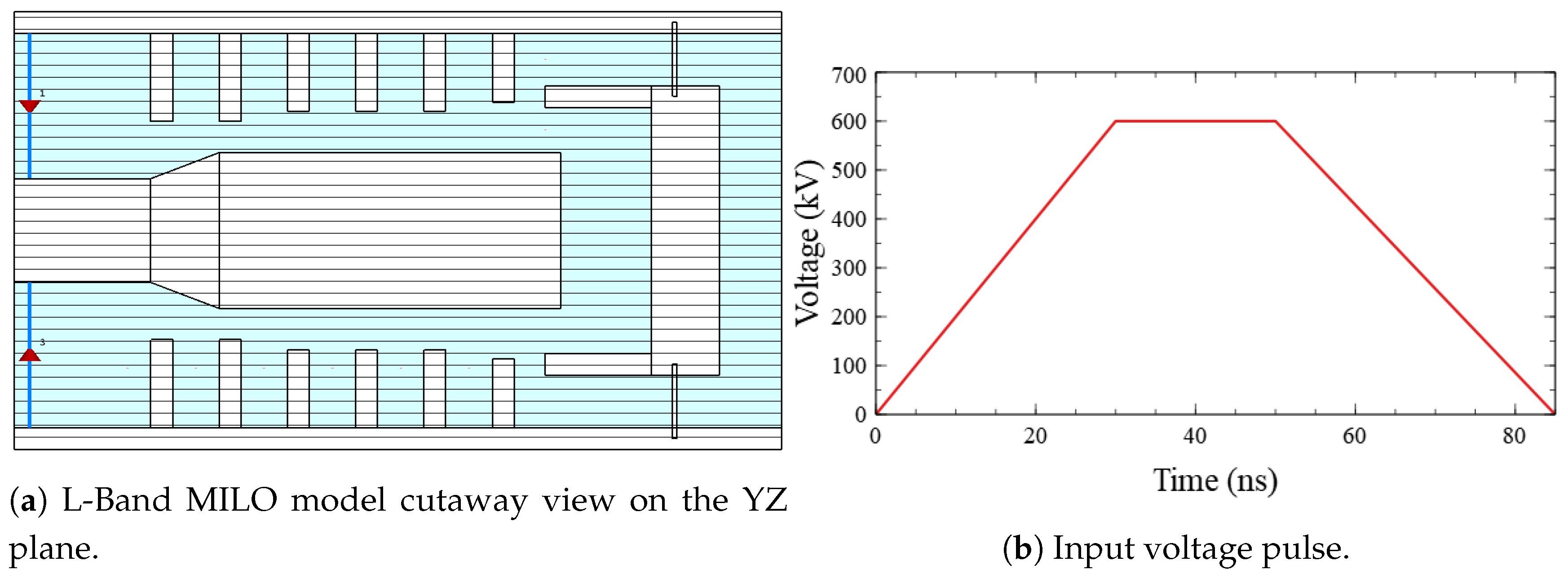
Figure 1.
(a) The three-dimensional view of an L-Band MILO. The boundary conditions used within the particle-in-cell (PIC) simulation display by color, blue for a magnetic boundary and green for an electric boundary. (b) List of critical component dimensions.
Figure 1.
(a) The three-dimensional view of an L-Band MILO. The boundary conditions used within the particle-in-cell (PIC) simulation display by color, blue for a magnetic boundary and green for an electric boundary. (b) List of critical component dimensions.

Figure 2.
(a) The two-dimensional representation of the MILO device on the YZ plane at the X origin. The input of the device, the left-side of the image, has a set of four discrete ports, spaced 90 degrees from each other, excited by the voltage pulse displayed in (b).
Figure 2.
(a) The two-dimensional representation of the MILO device on the YZ plane at the X origin. The input of the device, the left-side of the image, has a set of four discrete ports, spaced 90 degrees from each other, excited by the voltage pulse displayed in (b).

Figure 3.
(a) The two-dimensional representation of the MILO device on the YZ plane at the X origin. (b) List of critical component dimensions of the S-band MILO.
Figure 3.
(a) The two-dimensional representation of the MILO device on the YZ plane at the X origin. (b) List of critical component dimensions of the S-band MILO.

Figure 4.
The S-Band MILO with color indicating the location and type of material applied to the model.
Figure 4.
The S-Band MILO with color indicating the location and type of material applied to the model.

Figure 5.
The schematic of the circuit used for the co-simulation within CST studio suite. The Marx generator is designed to match closely to the theoretical impedance of the MILO, approximately 12 Ohms with an erected, open-circuit voltage of 1.2 MV. The yellow box is trigger signal which activates immediately upon the start of the co-simulation dumping the Marx energy into the MILO visible to it’s right.

Figure 6.
Center cut of the MILO model within CST studio suite with markers placed to indicating the parameters which are individually varied in four different parametric sweeps.
Figure 6.
Center cut of the MILO model within CST studio suite with markers placed to indicating the parameters which are individually varied in four different parametric sweeps.

Figure 7.
Calculated output characteristics of the L-band MILO. The results are obtained though a waveguide port placed at the output boundary of the model. The input voltage is an ideal trapezoidal pulse with a peak voltage of 600 kV.
Figure 7.
Calculated output characteristics of the L-band MILO. The results are obtained though a waveguide port placed at the output boundary of the model. The input voltage is an ideal trapezoidal pulse with a peak voltage of 600 kV.

Figure 8.
Measurement of the instantaneous output radio frequency (RF) power of the MILO with the figure on the left showing over the entire simulation runtime and right for a time where the power is at its peak. The results are obtained by integrating the three-dimensional power flow over a surface just before the output boundary of the model.

Figure 9.
The current waveform feeding the discrete ports which excite the MILO and the frequency analysis of the RF output. The total current is the summation of each of the plotted waveform, approximately 60 kA during peak draw.
Figure 9.
The current waveform feeding the discrete ports which excite the MILO and the frequency analysis of the RF output. The total current is the summation of each of the plotted waveform, approximately 60 kA during peak draw.

Figure 10.
Measurement of the instantaneous output RF power.

Figure 11.
Measured input current waveform through the discrete ports and the Fourier transform of the RF output.
Figure 11.
Measured input current waveform through the discrete ports and the Fourier transform of the RF output.

Figure 12.
Measured instantaneous power of the RF output of the MILO.

Figure 13.
Measured input current waveform through the discrete ports and the Fourier transform of the RF output.
Figure 13.
Measured input current waveform through the discrete ports and the Fourier transform of the RF output.

Figure 14.
The measured input waveforms which are fed to the MILO model during co-simulation of the device. These were measured by a monitor placed within the schematic model and compared to the recorded values from the PIC simulation.
Figure 14.
The measured input waveforms which are fed to the MILO model during co-simulation of the device. These were measured by a monitor placed within the schematic model and compared to the recorded values from the PIC simulation.

Figure 15.
Measured instantaneous power of the output RF signal of the MILO.

Figure 16.
Fourier analysis of the output signal frequency.

Figure 17.
Calculated instantaneous output RF power over a set for five different models with varying extractor gap distances.
Figure 17.
Calculated instantaneous output RF power over a set for five different models with varying extractor gap distances.

Figure 18.
The total input current and the frequency analysis of the output signal of parameter sweep of the extractor gap.
Figure 18.
The total input current and the frequency analysis of the output signal of parameter sweep of the extractor gap.

Figure 19.
Measurement of the instantaneous output RF power over a set for five different models with varying stub radius.
Figure 19.
Measurement of the instantaneous output RF power over a set for five different models with varying stub radius.

Figure 20.
The total input current and the frequency analysis of the output signal of parameter sweep of the stub radius.
Figure 20.
The total input current and the frequency analysis of the output signal of parameter sweep of the stub radius.

Figure 21.
Calculated instantaneous output RF power by varying the stub location.

Figure 22.
The total input current and the frequency analysis of the output signal of parameter sweep of the stub location.
Figure 22.
The total input current and the frequency analysis of the output signal of parameter sweep of the stub location.

Figure 23.
Calculated instantaneous output RF power by varying the cathode beam dump overlap.

Figure 24.
The total input current and the frequency analysis of the RF output of a parameter sweep of the cathode beam dump overlap.
Figure 24.
The total input current and the frequency analysis of the RF output of a parameter sweep of the cathode beam dump overlap.


Table 1.
The table of key parameter design equations.
| SWS fan radius | |
| Anode radius | |
| RF choke radius | |
| Extractor radius |
Table 2.
Conductivity of highly ordered pyrolytic graphite [5].
Table 2.
Conductivity of highly ordered pyrolytic graphite [5].
| Material Property | Value |
|---|---|
| Resistivity (AB) | 20,000 |
| Resistivity (C) | 200 |
© 2019 by the authors. Licensee MDPI, Basel, Switzerland. This article is an open access article distributed under the terms and conditions of the Creative Commons Attribution (CC BY) license (http://creativecommons.org/licenses/by/4.0/).
Share and Cite
MDPI and ACS Style
Abide, M.; Dickens, J.; Joshi, R.P.; Neuber, A.; Mankowski, J. Simulation of an S-Band MILO with Adjustable Beam Dump. Plasma 2019, 2, 138-155. https://doi.org/10.3390/plasma2020011
AMA Style
Abide M, Dickens J, Joshi RP, Neuber A, Mankowski J. Simulation of an S-Band MILO with Adjustable Beam Dump. Plasma. 2019; 2(2):138-155. https://doi.org/10.3390/plasma2020011
Chicago/Turabian StyleAbide, Matthew, James Dickens, Ravi P. Joshi, Andreas Neuber, and John Mankowski. 2019. "Simulation of an S-Band MILO with Adjustable Beam Dump" Plasma 2, no. 2: 138-155. https://doi.org/10.3390/plasma2020011