
SWOT Analysis of Electrical Discharge Coatings: A Case Study of Copper Coating on Titanium Alloy
by
 , and
, and
JagadeeswaraRao Maddu
1 ,
,
Buschaiah Karrolla
1,
Riyaaz Uddien Shaik
2,* and
Diana-Petronela Burdhuhos-Nergis
3 1
Department of Mechanical Engineering, University College of Engineering, Osmania University, Hyderabad 500007, India
2
Department of Astronautics Electrical and Energy Engineering, University of Rome “La Sapienza”, Via Eudossiana 18, 00184 Rome, Italy
3
Department of Materials Engineering and Industrial Safety, Faculty of Materials Science and Engineering, “Gheorghe Asachi” Technical University of Iasi, Professor Dimitrie Mangeron 67, 700050 Iași, Romania
*
Author to whom correspondence should be addressed.
Surfaces 2022, 5(2), 290-307; https://doi.org/10.3390/surfaces5020021
Submission received: 9 April 2022
/
Revised: 29 April 2022
/
Accepted: 6 May 2022
/
Published: 16 May 2022
(This article belongs to the Special Issue Surface Engineering and Phase Transformations in Metals and Alloys)
Abstract
:The electrical discharge machine (EDM) has been one of the most widely used non-traditional machines in recent decades, primarily used for machining hard materials into various complex shapes and different sizes and, nowadays, used for surface modifications/hard coatings. In this study, the SWOT (strengths, weaknesses, opportunities and threats) of electrical discharge coating was analyzed by conducting a case study. For the purpose of the case study, copper was deposited on the titanium alloy surface (Ti6Al4V). Three electrodes of different copper alloy materials, viz., brass, bronze and copper, were selected for coating the Ti6Al4V surface. Input parameters such as current, pulse-on, pulse-off, flushing pressure and the electrode material were optimized to develop a uniform coating. Experiments were designed according to the L18 orthogonal array, and among them, the samples that showed proper coating, as seen with the naked eye, were selected for morphological and elemental analyses by scanning electron microscopy (SEM) and energy-dispersive X-ray spectroscopy (EDX. Further, the output responses, viz., the material deposition rate (MDR), electrode wear rate (EWR), surface roughness (SR), elemental data (copper (Cu) and zinc (Zn)) and coating thickness (CT), were considered for the optimization of coatings. Implementing the Technique for Order Performance by Similarity to Ideal Solution, copper coating with a thickness of 20.43 µm, developed with an MDR with input parameters of 20 A current, 600 µs pulse-on, 120 µs pulse-off, 0.5 bar flushing pressure and the brass electrode, was selected as the optimum coating. The most influential parameters in this coating process were the current and pulse-on time. In this study, a SWOT table was developed to depict the strengths, weaknesses, opportunities and threats of electrical discharge coating.
1. Introduction
Electrical discharge coating (EDC) is a process used to improve and modify the surfaces of materials or workpieces in terms of mechanical, physical and biochemical properties. Researchers worldwide [1] are using this technique to create protective coatings that can withstand extreme temperatures, pressures and hostile environments. By doing so, the properties of the base material, such as strength [2], corrosion resistance [3], wear resistance [4], biocompatibility [5], etc., are increased. Nowadays, surface modification is also important in the biomedical area [6,7], specifically in dentistry [8] and orthopedic applications [2,9], to improve the biomechanical and morphological compatibilities between existing and newly introduced body tissues and to promote osteointegration [10]. Plasma-based surface modification can improve adhesion and surface wettability, minimize tissue surface friction and reduce contaminants to a safe level [11]. This is why previous research has consistently demonstrated the necessity of surface modification in the biomedical sector, particularly for modifying the surfaces of the outermost tissues and producing/fabricating a homogeneous implant surface [12,13].
In the past, there were many surface modification techniques, such as carburizing, electroplating, plasma spraying, etc., which are widely employed in today’s business [14]. However, in recent years, the use of EDC to alter material surfaces using electrical discharge energy has received interest as a result of recent breakthroughs in the field of surface modification. EDC is a novel technology that is derived from electrical discharge machining (EDM) by changing the polarity of the electrodes [15]. The electrode material is melted and deposited on the surface of the workpiece at an extremely high temperature (8000 °C to 12,000 °C) in EDC [16]. EDC can also modify the surfaces of all types of electrically conductive materials, including those that are exceedingly difficult to process, such as tungsten carbide and silicon carbide [17]. However, no literature is available on the thorough assessment of the fundamentals and applications of this extremely promising technology. Moreover, no comprehensive assessment has been reported on how the EDC process parameters will impact output process parameters such as the deposition rate, electrode wear rate, etc. To fill this gap, a systematic study was carried out to deposit copper on the titanium alloy (Ti6Al4V) surface and to then extract the strengths, weaknesses, opportunities and threats of EDC technology in the field of surface modification for high-function products [18,19,20].
S. L. Li et al. [21] developed an anti-wear coating deposited on H31 steel by considering the hierarchical aspects of TiC-enhanced cermet coating using different dielectric fluid mixing processes and evaluated micro-hardness (HV), wear and the coefficient of friction. A. F. Mansor et al. [22], in their paper, reported the effects of input parameters of EDC coating on the recast layer, crater size and surface roughness (SR) of TiNi shape memory alloy. The recast layer formation discharge duration was the most influential factor, and the peak current affected SR and crater size. A researcher from IIT Dhanbad [23] worked to improve the surface roughness and hardness of Ti6Al4V using brass electrodes by varying input parameters such as the powder concentration, voltage and duty factor of EDM. MoS2 powder was mixed in deionized water to improve the above-mentioned parameters. They also reported that powder concentration was the most influential parameter for layer deposition, and SR decreased and HV increased with the powder concentration. In another paper [24], it was reported that by modifying two input parameters, namely, electrode rotary speed and gas flow rate, cooling the electrode N2 gas and rotating the electrode equipment setup, calcium and phosphorous were incorporated into the coating on a titanium workpiece for corrosion resistance application. A. Kumar et al. [25] carried out their work by considering surface roughness, white layer thickness, micro-hardness and scatter crack density using an AlSI10 electrode on titanium alloy and AISI040. Their analysis concluded that surface characteristics were improved by using a rapid prototyping tool, whereas a low material removal rate was observed when using conventional electrodes, and the current was the most influential factor for micro-hardness. A. F. Mansor et al. [26], in their paper, reported that they analyzed nickel-titanium shape memory alloy using titanium and copper materials to optimize the output parameters of the recast layer thickness, crater size and surface roughness. The input parameters considered were discharge duration, pulse interval, peak current and gap voltage, which were optimized using ANOVA. For the recast layer formation, the discharge duration was the most influential factor, and the peak current had an effect on surface roughness. D. Sharma et al. [27] conducted a study to modify the surface of titanium alloy using hBN powder mixed in a dielectric on a micro-EDM machine. Input parameters such as voltage, duty factor and powder concentration were varied in their study to measure output parameters such as material deposition, surface roughness, hardness, wear coefficient and corrosion. V. D. Bui et al. [28] investigated an antibacterial coating on a Ti6Al4V by mixing silver nanopowder at different concentrations in a dielectric fluid of micro-powder mixed electrical discharge machine (PMEDM). The analysis concluded that the deep coating contained a lower silver powder concentration. R. Tyagi et al. [29] investigated the EDM-coated surface compared with an uncoated surface using a scanning electron microscope with energy-dispersive X-ray spectroscopy (EDX) characterization and conducted a wear test to analyze the wear. A paper authored by A. R. Siddique et al. [30] reported on the difficulty in coating localized areas using powder electrodes with micro-EDM. Their study concluded that the brass electrode showed a better coating, whereas the WS2–brass (70:30) electrode showed a uniform surface coating. V. D. Bui et al. [31] conducted another work to study the elemental composition of surface-modified materials, i.e., silver layer coating on Ti6Al4V, for antibacterial application. Another research group [32] reported their work on coating the SS304 surface by varying input parameters. A crack-free coating was obtained using different ceramics. Z. Y. Zeng et al. [33] conducted a comparative study between physical vapor deposition and electrical discharge coating (EDC) for TiNC and concluded that EDC provided the required coating in terms of thickness and wear. P. J. Liew et al. [34] conducted a review considering all of the previous research on electrical discharge coating techniques. Nuhaize et al. [35] conducted a study on the formation of electrical discharge coatings on stainless steel with an electrode of stellite 31. They concluded in their study that particle sizes between 45 and 70 microns were obtained. The same group of researchers conducted a study to analyze residual stress in EDCs and concluded that residual stresses ranged between +6 and −140 MPa [36]. Roshalliza et al. [37], in their study on electrical discharge coating of NiTi alloy in deionized water, analyzed surface roughness and concluded that improving the surface roughness of Nitinol will have applications in the biomedical field. Ahmad et al. [38] evaluated parameters for electrical discharge coatings on nickel–titanium shape memory alloy in deionized water and mentioned that the polarity of the electrode was found to have a significant influence on the recast layer.
This paper provides details on various issues and procedures involved in electrical discharge coatings; for example, reverse polarity (Tool + Workpiece−) is more effective than straight polarity (Tool – Workpiece+), adding a powder to a dielectric fluid can improve the coating deposition and reduce the formation of microcracks/holes, and the dry EDC process is the most eco-friendly process. The possibility of using powder metallurgy electrodes, etc., is also explored.
This work aimed to evaluate EDCs by SWOT (strengths, weaknesses, opportunities and threats) analysis. SWOT analysis is a cognitive process for studying the interrelations between the internal and external surroundings of processing. Based on the characterization of EDCs, an evaluation of strengths, weaknesses, opportunities and threats was performed. Combining these analysis strategies will serve to provide a solution for developing enhanced EDCs. Strengths in the SWOT analysis are internal capabilities and positive factors that are relevant to the objectives and applications [20]. Weaknesses are internal factors or constraints that impede or hinder the performance of EDC. Therefore, the strengths and weaknesses are internal elements. Opportunities in the SWOT analysis are factors or features that facilitate the business establishment by connecting it with outside organizations. Threats deal with negative factors external to electrical discharge coating, which can hinder or delay achievable goals. The latter two are external factors, and EDC can exploit their differences. As such, opportunities and threats are viewed as environmental factors. In this work, firstly, a SWOT matrix was formed for the internal and external factors involved in electrical discharge coatings. To form a matrix, a case study was required, for which copper coating using an electrical discharge machine was chosen.
Reviewing the literature, it was observed that no SWOT analysis has been conducted on the electrical discharge coating process. SWOT analysis is used in most businesses to know the strengths, weaknesses, opportunities and threats of a system. In this work, a case study was conducted by depositing copper on a titanium alloy surface using different electrodes to understand the strengths, weaknesses, opportunities and threats of this process. Then, output parameters such as the material deposition rate, electrode wear, surface roughness, coating thickness and elemental composition were optimized. The main objectives of this study were to (1) conduct a case study by coating using an electrical discharge machine and (2) create a SWOT matrix showing the strengths, weaknesses, opportunities and threats of this coating.
2. Materials and Methods
2.1. Materials
A titanium alloy-based workpiece was chosen as the base material for the copper coating for antibacterial applications. The samples of titanium alloy substrate were cut to 20 mm × 20 mm × 8 mm in size, and electrodes of copper, bronze and brass with dimensions of 100 mm in length and diameter of 10 mm were chosen, along with EDM 30 as dielectric fluid.
Table 1 displays the electrode and substrate’s chemical composition, density (kg/m2), melting point (°C), specific heat capacity (J/g °C) and hardness [2]. Table 2 shows the chemical composition of electrode materials, whereas Table 3 shows the physical properties of electrode and substrate.
Table 4 shows the experimental levels of the input parameters, viz., current, pulse-on (Ton), pulse-off (Toff), electrode materials and flushing pressure, formed using the Taguchi method [39].
Influence of Parameters on Electrical Discharge Coatings
The input parameters, namely, current, Ton, Toff, flushing pressure and electrode material, determine the topography, surface quality and homogeneity of the coatings. Table 4 lists the experimental input parameters, whereas Table 5 lists their combination. The Taguchi L18 design was used to create a combination of parameters, which were then manually changed depending upon the coating deposition [7,40]. Substrate and electrode materials tend to experience extremely high temperatures of around 10,000 degrees, which melt the electrode material and deposit it on the surface of the workpiece. This deposition per minute is called the material deposition rate (MDR), similar to the electrode wear rate (EWR). This material deposition rate is the ratio of weights measured after and before the machining to the time taken for machining.
where WAM = workpiece weight after machining, and WBM = workpiece weight before machining.
where EAM = electrode weight after machining, and EBM = electrode weight before machining. Electrode wear rate is the ratio of weights measured after and before machining to the time taken for machining.
2.2. Methods
2.2.1. Technique for Order of Preference by Similarity to Ideal Solution (TOPSIS)
The traditional Taguchi approach is insufficient to solve a multi-response optimization problem [41]. To overcome this limitation, a multi-criteria decision-making method and Technique for Order of Preference by Similarity to Ideal Solution (TOPSIS) were applied in the present study. To optimize the process parameters to obtain the optimum results, TOPSIS was applied in a stepwise manner, as shown in Table 5 [15].

Table 5.
TOPSIS Equations.
| Step No. | Steps | |
|---|---|---|
| 1 | In this method, the first step is to develop a decision matrix. This method consists of alternatives in the rows and attributes in the columns. The matrix format can be expressed as [42]: | |
| (3) | ||
| a (i = 1, 2, 3, …, m) represents all possible alternatives, X (j = 1, 2, 3, …, n) represents the attributes related to performance of alternatives, j = 1, 2, 3, …, n, and Xij represents the performance of i with respect to attribute j. | ||
| 2 | In this step, the above decision matrix is normalized, and we obtain a normalized decision matrix . The formula for is given below the normalized decision matrix . | |
| (4) | ||
| 3 | The weighted normalized decision matrix can be calculated by using the formula , and we obtain a weighted normalized decision matrix. | |
| (5) | ||
| (6) | ||
| 4 | Here, positive ideal solutions (best) and negative ideal solutions (worst) need to be calculated in this step. The solutions can be represented as the positive ideal (best) solution. | |
| (7) | ||
J and J’ are associated with beneficial and non-beneficial attributes. | (8) | |
| 5 | Now, it is necessary to calculate the Euclidean distance of each alternative from positive ideal and negative ideal solutions by using the following equations: | |
| (9) | ||
| (10) | ||
| 6 | The calculation of the relative closeness to the ideal solution for each alternative by using the equation is given below. | |
| (11) | ||
| 7 | Here, the results are ranked according to the preference order. The alternative with maximum relative closeness should be the best choice. is termed multi-performance characteristic index (MPCI) in TOPSIS. Following the steps described in this section, optimization can be carried out for the output parameters to select an optimum coating. | |
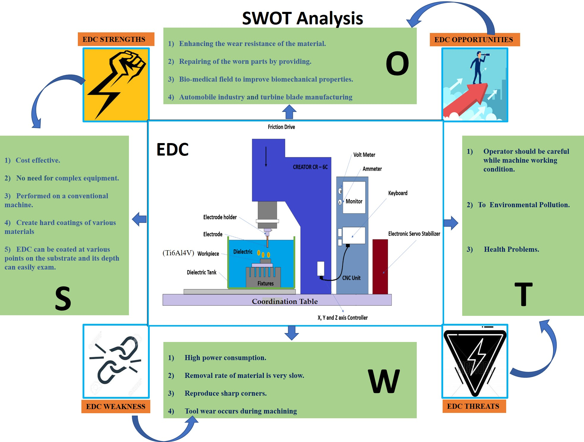
2.2.2. The Coating Process
The flow of the coating process is depicted in Figure 1. A titanium plate was procured from Ramesh Steels Corporation Pvt. Ltd., Mumbai, India, and then wire-cut EDM was used to cut it into substrates with the required size of 300 mm × 450 mm × 8 mm. The substrates were then ground and polished using 50-, 100-, and 200-micron emery paper; after completion, the substrates were used in the above-mentioned treatments. The electrodes were sliced into a length of 100 mm after obtaining the requisite diameter. The Production Engineering Lab at Osmania University has a CNC Sinker EDM (Creator CR-6C, Taipei, Taiwan) with different electrodes (such as copper, brass and bronze) and ED 30 oil as dielectric fluid.
Table 6 depicts the six experiments selected from the L18 orthogonal array, and these coatings were selected since they are visible to the naked eye. The input parameters of these eighteen experiments are shown in Table 6, and their coatings will be shown in following figures. These coatings were taken for characterization to select the optimum coating.
The output parameters for all of the trial combinations are listed in Table 4. The weight of the substrate before (A) and after (B) is represented by the letters A and B. Electrode deposition rate, on the other hand, is the ratio of the change in substrate weight (before and after machining) to the time taken.
After the deposition, in addition to material deposition rate and electrode wear rate, surface roughness was also measured using a Surftester (model SJ301, Mitutoyo South East Asia Pvt. Ltd., New Delhi, India), as shown in Figure 1. Surface roughness is one of the output process parameters. Coating thickness, which is also an output process parameter, was measured using the SEM attached to the EDAX instrument (model JCM-6000PLUS, JEOL Ltd., Tokyo, Japan). Similarly, microcracks were also measured using SEM, and the results obtained from these measurements and characterizations are explained in the following section.
3. Results
3.1. Output Process Parameters
As described in Section 2.2.2, experiments were conducted, and the output process parameters were obtained for all of the experiments. Table 7 shows the output values obtained for each parameter, i.e., MDR, EWR, CT, Cu%, Zn% and MC. Among the 18 experiments (EX), only the substrates that had the optimum coating were selected and are shown in Table 6. It can be observed from this table that the coating thickness varied between 19 and 29 microns, whereas microcracks were from 0.1 to 4 microns.
3.2. Elemental Analysis
SEM with energy-dispersive X-ray spectroscopy was used to examine the chemical compositions of the coatings. Figure 2 shows the EDX results with SEM images of the coating deposited using the indicated parameters. Experiment 6 had a higher copper percentage (84.56%) compared with the bronze electrode, and the input parameters were the current (30), Ton (600), Toff (120) and flushing pressure (0).
TOPSIS is a stepwise process like grey relational analysis and involves seven steps. The formulae that were utilized to compute each step are listed in the previous section. The first step in this procedure is to create a matrix using the output parameters. It enables the faster and easier processing of data. The next step is to assign weights to the parameters; however, since all of the parameters were given equal weight, this step was skipped. The decision matrix was created for TOPSIS using Table 7.
Subsequently, the normalization of values is performed for the above-normalized decision matrix. Various attribute dimensions are transformed into non-dimensional units to make inter-attribute comparisons easier. The values in Table 8 were obtained using Equation (9) as a guide.
Because all of the output parameters were given an equal weighting of 0.25, each value in Table 4 was multiplied by 0.25, and the normalized decision matrix is shown in Table 9.
The positive ideal solution decreases the cost criteria while increasing the benefit criteria; the negative ideal solution, on the other hand, enhances the cost criteria while decreasing the benefit criteria. As stated in Table 10, the parameters that are needed were considered positive ideal solutions (maximum of all parameters), while those that are not needed were considered negative ideal solutions (minimum of all parameters).
The distance measure from the positive and negative ideal solutions was obtained in this stage and is presented in Table 11. As indicated in Equations (9) and (10), D+ and D− represent distances from positive and negative solutions, respectively.
The final step is to use the calculations in Equation (11) to compute the relative closeness. Table 12 shows the results, and it can be seen that experiment 5 has a lower closeness and is ranked first.
3.3. Study of Surface Morphology
SEM images of a total of six experiments are shown in Figure 3, and the effects of input parameters on the coating surface can be observed in this figure.
From these figures, it can be observed that the current has a major impact on the coating surface. The surface becomes smoother with the decrease in current. Figure 3a has a smoother surface in comparison with other surfaces. The other input parameters are shown in the SEM image itself as an inset.
The machining spatter that occurs due to the high flushing pressure of 1 bar is another reason for irregular surfaces. It was observed that with a reduction in flushing pressure and melting of the electrode (due to high current of 10 A and 20 A), the machining spatter was reduced and led to better surface coating.
The thickness of the coating at three random locations on the cross-section of the substrate is shown in the SEM picture, which is illustrated in the following figures, and the thickness in the table is the average of three thicknesses.
3.4. Layer Thickness
The investigation of coatings on substrates that were mechanically polished and chemically etched coatings was carried out using a scanning electron microscope. To check the thicknesses, cross-sections of substrates were scanned, and variations in thicknesses at different locations were observed. The cross-sectional edge of a coated part of a sample produced under the various conditions mentioned above is shown and explained in following section. It was assumed that the increase in the current and pulse-on increases the thickness of the coating but results in surface microcracks as shown in Figure 4.
Figure 5 exhibits SEM images of the cross-sections of substrates, together with a corresponding line for layer thickness. With the decrease in the values of input variables (current 20 A, Ton 600 µs, Toff 120 µs and bronze electrode), the layers become thicker (Figure 5c from 25.8 µm to 30.7 µm) and more discontinuous and lead to microcracks (current 10 A, Ton 400 µs, Toff 80 µs and bronze electrode).
3.5. Material Interfacing
Figure 6 shows a SEM cross-section that was prepared by cutting the substrate, depositing the coating using wire EDM and then polishing the substrate to provide insight into the fine-scale microstructure. From the SEM images, the base material and coating interface in all six experiments can be observed. Though a variation in the thickness of coatings can be observed, the interface looks uniform throughout the substrate.
The specimens in the images were obtained with a current of 20 A, Ton of 600 µs, Toff of 120 µs, flushing pressure of 0.5 bar and brass as the electrode material.
With detailed observation, a variation in the flatness of the base material can be observed, which is due to the time lag between sparks occurring between the substrate and coating. In the process of coating in EDC, firstly, the material will be slightly removed, and then the material will be deposited, which can be observed in Figure 6 in all SEM images.
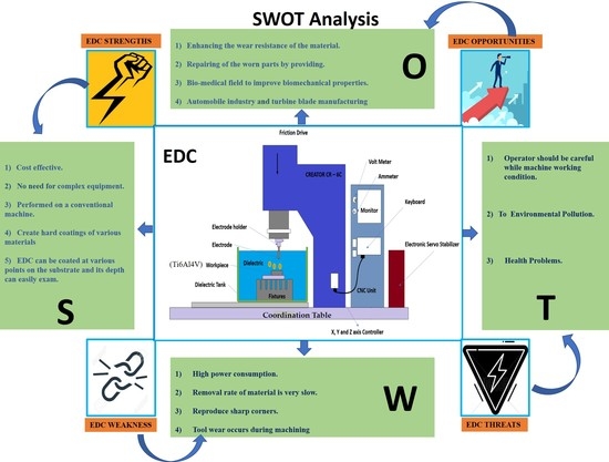
4. SWOT
As described in the Introduction section, SWOT stands for strengths–weaknesses–opportunities–threats. In this section, SWOT for electrical discharge coatings is shown. Previously, there was no literature that reported SWOT for EDC.
Usually, for small and medium-sized strategic planning, this form of analysis is used. Furthermore, some academics believe that SWOT analysis might be an effective technique for development and strategic industrialization. A SWOT analysis was conducted to identify areas of interest for the establishment of a biomedical application strategy and strategic environmental assessment for surface modification. The goal of this form of analysis is to create a qualitative process structure that identifies changes in the quantitative structure of the system under study, as well as the primary strengths, weaknesses, opportunities and threats. Overall, a SWOT analysis aids in the identification of a strategy’s strengths and weaknesses in achieving its objectives, as well as possibilities to lessen the impact on the objectives. Figure 7 depicts the points that were extracted by SWOT analysis in this study.
5. Discussion
In this work, an electrical discharge machine was used for coating copper material on titanium alloy. To deposit the copper coating, an evaluation was carried out using three different electrodes, and it was observed that the brass electrode provided uniform and crack-free coatings. Taguchi’s design of experiments was implemented to conduct experiments at different levels in the L18 orthogonal array. Of these 18 experiments, 6 experiments resulted in uniform coatings, so these coatings were chosen for characterization and further optimization. Upon TOPIS optimization, one experiment was chosen that demonstrated the optimum coating (thickness of 20.43667 µs) and input parameters (current of 20 A, Ton of 600 µs, Toff of 120 µs, flushing pressure of 0.5 bar and brass as electrode material). An optimum coating was obtained with mid-level current and a high level of pulse-on time. The current in EDC was directly proportional to thermal energy, and a long time of exposure to thermal energy led to the melting and deposition of electrode material on the substrate.
SWOT analysis was conducted to understand the strengths, weaknesses, opportunities and threats. A SWOT matrix is presented in Section 4, and a discussion of the SWOT matrix is provided in the following.
5.1. EDC Strengths
Electrical discharge coatings have proven strengths, and researchers worldwide are still working to extend the applications of EDC in various fields. The optimization of coating according to input parameters is still under development to further improve this coating technique. Standards for controlling input parameters to obtain certain coating thickness are lacking, but in comparison with weaknesses, this technique has several strengths, which are as follows:
- (1)
- Electrical discharge coating is a cost-effective technique in comparison with other coating methods [43]. The cost of the machine is the major cost of this process.
- (2)
- Electrical discharge coating is carried out on a well-established machine, the ‘Electrical Discharge Machine’, which is mostly used for drilling, machining complex shapes and hard materials, etc. [29,44]. Since this machine is available in most universities, further research on electrical discharge coating is possible, and it could lead to the standardization of the procedure.
- (3)
- In addition, the coating can be deposited conventionally without power metallurgy electrodes/powder mixed in a dielectric fluid, etc., just by using conventional electrodes readily available in the market [45]. Though many researchers have coated material using powder metallurgy/powder mixed in a dielectric medium, the case study presented in this paper proved that it can be coated using conventional electrodes.
- (4)
- In comparison with other coating methods, it is possible to coat hard materials. Liew et al. [46], in their paper, commented that the electrical discharge coating process can coat hard materials, which is also described in the Introduction section.
- (5)
- Depth can be administered using the numerical controls available on an electrical discharge machine, whereas for other coating methods, such as physical vapor deposition (PVD), chemical vapor deposition (CVD), etc., a special apparatus is required for control. For example, PVD coating needs a vacuum setup to control the machine surface [42,44].
5.2. EDC Opportunities
Various opportunities are available when an electrical discharge machine is used for coating purposes.
- (1)
- This technique can be used for surface modifications both without coating and with coating. It has the exceptional characteristic that it can be carried on any hard material [47].
- (2)
- The wear resistance of the hard material can also be improved, or if the surface is already worn out, it can be repaired [48].
- (3)
- This coating has applications in various fields, such as biomedicine [12], aerospace [49] and turbine blades [12]. The surface adjustment was carried out by modifying the center to obtain a thick and permeable oxide layer on the surface of restorative Ti inserts to improve tissue development and quicken recuperation. In some cases, due to cleaning, handling and grinding, the oxide coatings can disintegrate over time. In such situations, electrical discharge coatings have the awesome potential of utilizing oxide layers to functionalize the surface [50]. Additionally, EDC has the potential to make strides in improving the biocompatibility of Ti6Al4V with human bones and teeth by depositing a layer of perovskite Ti (CaTiO3) [14].
5.3. EDC Weaknesses
Though electrical discharge coating is useful in various applications, it also has some weaknesses that can be overcome. Some of them are listed here as follows:
- (1)
- In the modern world, most coating equipment requires power. Similarly, this technique is completely based on power, without which coating cannot be deposited.
- (2)
- (3)
- This technique cannot reproduce sharp corners of a substrate for complex shapes. Thus, complex shapes with sharp corners cannot be coated using this technique.
- (4)
- There will be a high loss in the deposition of electrode material. Most of the material remains in the dielectric fluid, as observed in our case study.
- (5)
- Due to the mixture of electrode and workpiece materials remaining in the dielectric fluid, the filtration time is longer in comparison with other processes, such as drilling, machining, etc., on electrical discharge machines. The filtration time increases from 2 to 3 h when depositing a copper coating on titanium alloy.
- (6)
- The complete process should be carried out in one run, or else it will lead to defects when re-running. Defects will be cracks, irregular surfaces, etc., Moreover, it is not possible to continue from an earlier stopping point.
5.4. EDC Threats
There are not many threats connected with electrical discharge coating. Some of them are as follows:
- (1)
- Technicians working with this machine have to be careful by using the necessary gloves, etc. A fire can erupt in a conventional EDC operation, damaging the building and equipment, interrupting business and delaying deliveries to customers. Operators should be warned of the potential of fires in the machine to spread when blowing the burning dielectric fluid in the tank with an extinguisher. Sometimes, extreme care is also necessary to prevent blasting the flame in the direction of anyone assisting with the fire.
- (2)
- Technicians have to be skilled to code the program for the computer numerically controlled electrical discharge machine. EDM operators need to be trained adequately beforehand concerning safe procedures for setup and operation, the maintenance of the integrity of fire protection systems and the need to monitor operations.
- (3)
- Environmental pollution is another threat with any kind of machinery. This technique will pollute the environment when dielectric fluid is disposed of, and while working with the machines, it will cause air pollution. An EDM machine usually generates flammable gases during machining. The quantities and types of gases produced vary depending upon the material being machined, dielectric fluid, operating temperature, current and voltage.
- (4)
- There are possible health issues for people working with this machine.
6. Conclusions
In this study, titanium alloy (Ti6Al4V) was coated with copper using three different electrodes, viz., brass, bronze and copper. In the future, it is planned to optimize the coatings (more uniform and crack-free) by using different surface modification techniques. An optimum coating thickness was observed on the titanium substrate coated with a brass electrode, which may be due to its lower melting point in comparison with other electrode materials. From this study, the following conclusions can be presented:
- -
- To select an optimum coating, optimization was carried out using the TOPSIS method.
- -
- Experiments with input parameters (current of 20 A, Ton of 600 µs, Toff of 120 µs, flushing pressure of 0.5 bar and brass as electrode material) having output responses (material deposition rate of 0.85778 mm2/min, electrode wear rate of 24.6488 g/min, surface roughness of 9.02 µm, coating thickness of 20.43666667 µm, copper of 76.25% and zinc 11.19%) were selected as a high priority (rank 1) in the TOPSIS method.
- -
- Finally, SWOT analysis was carried out by performing an experiment as a case study and also by referring to the relevant literature. A matrix showing the strengths, weaknesses, opportunities and threats is explained. Every process will have weaknesses and threats, but the main point to be considered is whether it is possible to overcome them or not. In this process, it can be concluded that it is possible to overcome most of the weaknesses and threats, and in the future, EDM will become multi-purpose equipment upon further research.
Author Contributions
Conceptualization, J.M. and R.U.S.; methodology, J.M. and R.U.S.; software, J.M. and R.U.S.; validation, R.U.S. and J.M.; formal analysis, J.M.; investigation, J.M.; resources, B.K.; data curation, J.M.; writing—original draft preparation, J.M. and R.U.S.; writing—review and editing, R.U.S. and D.-P.B.-N.; visualization, J.M. and R.U.S.; supervision, B.K.; project administration, J.M. and R.U.S.; funding acquisition, B.K. All authors have read and agreed to the published version of the manuscript.
Funding
This research received no external funding.
Acknowledgments
The authors would like to thank S. Arun Kumar, Technician, Production Lab, A. Krishnaiah, Production Lab In-Charge, and Rega Rajendra, Head, Department of Mechanical Engineering, University College of Engineering, Osmania University, for their full support in conducting experiments. The authors also thank Sampath Kumar, Virtue Meta-Sol, Hyderabad, for support in characterization.
Conflicts of Interest
The authors declare no conflict of interest.
References
- Al-Amin, M.; Rani, A.M.A.; Aliyu, A.A.A.; Razak, M.A.A.; Hastuty, S.; Bryant, M.G. Powder mixed-EDM for potential biomedical applications: A critical review. In Materials and Manufacturing Processes; Bellwether Publishing, Ltd.: Columbia, MD, USA, 2020; pp. 1789–1811. [Google Scholar] [CrossRef]
- Stráský, J.; Janeček, M.; Harcuba, P.; Bukovina, M.; Wagner, L. The effect of microstructure on fatigue performance of Ti-6Al-4V alloy after EDM surface treatment for application in orthopaedics. J. Mech. Behav. Biomed. Mater. 2011, 4, 1955–1962. [Google Scholar] [CrossRef] [PubMed]
- Davoodi, A.; Pakshir, M.; Babaiee, M.; Ebrahimi, G.R. A comparative H2S corrosion study of 304L and 316L stainless steels in acidic media. Corros. Sci. 2011, 53, 399–408. [Google Scholar] [CrossRef]
- Algodi, S.J.; Murray, J.W.; Brown, P.D.; Clare, A.T. Wear performance of TiC/Fe cermet electrical discharge coatings. Wear 2018, 402–403, 109–123. [Google Scholar] [CrossRef]
- Lee, B.E.J.; Ho, S.; Mestres, G.; Karlsson, M.; Koshy, P.; Grand, K. Surface & Coatings Technology Dual-topography electrical discharge machining of titanium to improve biocompatibility. Surf. Coat. Technol. 2016, 296, 149–156. [Google Scholar] [CrossRef]
- Liew, P.J.; Yap, C.Y.; Wang, J.; Zhou, T.; Yan, J. Surface modification and functionalization by electrical discharge coating: A comprehensive review. Int. J. Extrem. Manuf. 2020, 2, 12004. [Google Scholar] [CrossRef]
- Maddu, J.; Shaik, R.U. A Review on Electrical Discharge Coating (EDC) and its Multi-Optimization Techniques. IOP Conf. Ser. Mater. Sci. Eng. 2021, 1185, 12027. [Google Scholar] [CrossRef]
- Richardson, M.T.; Gianchandani, Y.B. Achieving precision in high density batch mode micro-electro-discharge machining. J. Micromech. Microeng. 2008, 18, 15002. [Google Scholar] [CrossRef] [Green Version]
- Harcuba, P.; Bačáková, L.; Stráský, J.; Bačáková, M.; Novotná, K.; Janeček, M. Surface treatment by electric discharge machining of Ti-6Al-4V alloy for potential application in orthopaedics. J. Mech. Behav. Biomed. Mater. 2012, 7, 96–105. [Google Scholar] [CrossRef]
- Arun, I.; Yuvaraj, C.; Selvarani, P.; Senthilkumaar, J.S.; Thamizhmanii, S.; Muruganandam, P. Synthesis of electrical discharge metal matrix composite coating through compacted semi-sintered electrode and its tribological studies. J. Braz. Soc. Mech. Sci. Eng. 2019, 41, 213. [Google Scholar] [CrossRef]
- Hsu, H.Y.; Hu, C.C. Surface quality improvement of EDMed Ti–6Al–4V alloy using plasma etching and TiN coating. Int. J. Adv. Manuf. Technol. 2017, 88, 67–74. [Google Scholar] [CrossRef]
- Sales, W.F.; Oliveira, A.R.F.; Raslan, A.A. Titanium perovskite (CaTiO3) formation in Ti6Al4V alloy using the electrical discharge machining process for biomedical applications. Surf. Coat. Technol. 2016, 307, 1011–1015. [Google Scholar] [CrossRef]
- Mughal, M.P.; Farooq, M.U.; Mumtaz, J.; Mia, M.; Shareef, M.; Javed, M.; Jamil, M.; Pruncu, C.I. Surface modification for osseointegration of Ti6Al4V ELI using powder mixed sinking EDM. J. Mech. Behav. Biomed. Mater. 2021, 113, 104145. [Google Scholar] [CrossRef]
- Khan, M.Y.; Rao, P.S.; Pabla, B.S. A Framework for Surface Modification by Electrical Discharge Coating using Variable Density Electrodes. E3S Web Conf. 2021, 309, 1093. [Google Scholar] [CrossRef]
- Maddu, J.; Vuppala, S.; Shaik, R.U. Formation and Statistical Optimization of Electrical Discharge 2 Coatings using Conventional Electrodes. Energies 2021, 14, 5691. [Google Scholar] [CrossRef]
- Algodi, S.J.; Clare, A.T.; Brown, P.D. Modelling of single spark interactions during electrical discharge coating. J. Mater. Processing Technol. 2018, 252, 760–772. [Google Scholar] [CrossRef]
- Janmanee, P.; Muttamara, A. Surface modification of tungsten carbide by electrical discharge coating (EDC) using a titanium powder suspension. Appl. Surf. Sci. 2012, 258, 7255–7265. [Google Scholar] [CrossRef]
- Prakash, C.; Kansal, H.K.; Pabla, B.; Puri, S.; Aggarwal, A. Electric discharge machining—A potential choice for surface modification of metallic implants for orthopedic applications: A review. Proc. Inst. Mech. Eng. Part B 2016, 230, 331–353. [Google Scholar] [CrossRef]
- Prakash, C.; Singh, S.; Pruncu, C.I.; Mishra, V.; Królczyk, G.; Pimenov, D.Y.; Pramanik, A. Surface modification of Ti-6Al-4V alloy by electrical discharge coating process using partially sintered Ti-Nb electrode. Materials 2019, 12, 1006. [Google Scholar] [CrossRef] [Green Version]
- Nezhad, M.M.; Shaik, R.U.; Heydari, A.; Razmjoo, A.; Arslan, N.; Garcia, D.A. A SWOT analysis for offshore wind energy assessment using remote-sensing potential. Appl. Sci. 2020, 10, 6398. [Google Scholar] [CrossRef]
- Li, S.L.; Mai, Y.J.; Huang, M.Y.; Jie, X.H. Anti-wear hierarchical TiC enhanced cermet coating obtained via electrical discharge coating using a reduced graphene oxide nanosheets mixed dielectric. Ceram. Int. 2020, 46, 11933–11942. [Google Scholar] [CrossRef]
- Mansor, A.F.; Azmi, A.I.; Zahiruddin, M.; Islam, M.N. Performance study of biocompatible recast layer formation on Ti6Al4V by using electrical discharge coatings. Int. J. Automot. Mech. Eng. 2020, 17, 7935–7941. [Google Scholar] [CrossRef]
- Mohanty, S.; Bhushan, B.; Das, A.K.; Dixit, A.R. A study on parametric optimization of Micro-electrical discharge coating process using response surface methodology. Mater. Today Proc. 2020, 38, 325–332. [Google Scholar] [CrossRef]
- Yu, Y.T.; Hsieh, S.F.; Lin, M.H.; Huang, J.W.; Ou, S.F. Improvement in Ca and P incorporation in the coating on Ti by gas-assisted electrical discharge coating. Surf. Coat. Technol. 2020, 400, 126120. [Google Scholar] [CrossRef]
- Kumar, A.; Siba, S.; Mahapatra, S. Surface Characteristics of EDMed Titanium Alloy and AISI 1040 Steel Workpieces Using Rapid Tool Electrode. Arab. J. Sci. Eng. 2020, 45, 699–718. [Google Scholar] [CrossRef]
- Mansor, A.F.; Azmi, A.I.; Zain, M.Z.M.; Jamaluddin, R. Parametric evaluation of electrical discharge coatings on nickel-titanium shape memory alloy in deionized water. Heliyon 2020, 6, e04812. [Google Scholar] [CrossRef]
- Sharma, D.; Mohanty, S.; Das, A.K. Surface modification of titanium alloy using hBN powder mixed dielectric through micro-electric discharge machining. Surf. Coat. Technol. 2020, 381, 125157. [Google Scholar] [CrossRef]
- Bui, V.D.; Mwangi, J.W.; Meinshausen, A.K.; Mueller, A.J.; Bertrand, J.; Schubert, A. Antibacterial coating of Ti-6Al-4V surfaces using silver nano-powder mixed electrical discharge machining. Surf. Coat. Technol. 2020, 383, 125254. [Google Scholar] [CrossRef]
- Tyagi, R.; Das, A.K.; Mandal, A. Electrical discharge coating using WS2 and Cu powder mixture for solid lubrication and enhanced tribological performance. Tribol. Int. 2018, 120, 80–92. [Google Scholar] [CrossRef]
- Siddique, A.R.; Mohanty, S.; Das, A.K. Micro-electrical discharge coating of Titanium alloy using WS2 and Brass P/M electrode. Mater. Manuf. Processes 2019, 34, 1761–1774. [Google Scholar] [CrossRef]
- Bui, V.D.; Mwangi, J.W.; Schubert, A. Powder mixed electrical discharge machining for antibacterial coating on titanium implant surfaces. J. Manuf. Processes 2019, 44, 261–270. [Google Scholar] [CrossRef]
- Murray, J.W.; Cook, R.B.; Senin, N.; Algodi, S.J.; Clare, A.T. Defect-free TiC/Si multi-layer electrical discharge coatings. Mater. Des. 2018, 155, 352–365. [Google Scholar] [CrossRef] [Green Version]
- Zeng, Z.Y.; Xiao, H.Q.; Jie, X.H.; Zhang, Y.M. Friction and wear behaviors of TiCN coating based on electrical discharge coating. Trans. Nonferrous Met. Soc. China 2015, 25, 3716–3722. [Google Scholar] [CrossRef]
- Panda, R.C.; Sharada, A.; Samanta, L.D. A review on electrical discharge machining and its characterization. Mater. Today Proc. 2021, in press. [Google Scholar] [CrossRef]
- Ahmed, N.; Murray, J.W.; Yuzawa, T.; Nakagawa, T.; Sarugaku, S.; Saito, D.; Brown, P.D.; Clare, A.T. Formation of thick electrical discharge coatings. J. Mater. Processing Technol. 2020, 285, 116801. [Google Scholar] [CrossRef]
- Ahmed, N.; Murray, J.W.; Yuzawa, T.; Kurokawa, T.; Nakagawa, T.; Sarugaku, S.; Saito, D.; Clare, A.T. Residual stress in electrical discharge coatings. Surf. Coat. Technol. 2021, 416, 127156. [Google Scholar] [CrossRef]
- Jamaluddin, R.; Lih, T.C.; Mansor, A.F.; Azmi, A.I.; Hamidon, R. Surface roughness analysis of NiTi alloy in electrical discharge coating process. IOP Conf. Ser. Mater. Sci. Eng. 2020, 932, 12120. [Google Scholar] [CrossRef]
- Mirzamohammadi, S.; Rouhaghdam, A.S.; Hadavi, S.M.M.; Aliofkhazraei, M. Nickel aluminide coating produced on γ-TiAl alloy by high activity aluminising process. Mater. Sci. Tech. 2011, 27, 1328–1332. [Google Scholar] [CrossRef]
- Buschaiah, K.; JagadeeswaraRao, M.; Chandra Sekhar Reddy, M. Optimization of Machining Parameter for EDM Using Taguchi Method on Incoloy-800. Int. J. Res. Eng. Appl. Sci. 2016, 6, 119–133. [Google Scholar]
- Maddu, J.; Karrolla, B.; Shaik, R.U.; Vuppala, S. Comparative Study of Optimization Models for Evaluation of EDM Process Parameters on Ti-6Al-4V. Modelling 2021, 2, 555–566. [Google Scholar] [CrossRef]
- Buschaiah, K.; JagadeeswaraRao, M.; Krishnaiah, A. Investigation on the influence of EDM parameters on machining characteristics for Aisi 304. Mater. Today Proc. 2018, 5, 1. [Google Scholar] [CrossRef]
- Kumar, D.; Mondal, S. Process parameters optimization of AISI M2 steel in EDM using Taguchi based TOPSIS and GRA. Mater. Today Proc. 2019, 26, 2477–2481. [Google Scholar] [CrossRef]
- Chakraborty, S.; Kar, S.; Dey, V.; Ghosh, S.K. Optimization and surface modification of Al-6351 alloy using Sic-Cu green compact electrode by electro discharge coating process. Surf. Rev. Lett. 2017, 24, 1750007. [Google Scholar] [CrossRef]
- Dwivedi, A.P.; Choudhury, S.K. Increasing the performance of EDM Process using tool rotation methodology for machining AISI D3 steel. Procedia CIRP 2016, 46, 131–134. [Google Scholar] [CrossRef] [Green Version]
- Wang, Z.L.; Fang, Y.; Wu, P.N.; Zhao, W.S.; Cheng, K. Surface modification process by electrical discharge machining with a Ti powder green compact electrode. J. Mater. Processing Technol. 2002, 129, 139–142. [Google Scholar] [CrossRef]
- Taherkhani, A.; Ilani, M.A.; Ebrahimi, F.; Huu, P.N.; Long, B.T.; Van Dong, P.; Tam, N.C.; Minh, N.D.; Van Duc, N. Investigation of surface quality in Cost of Goods Manufactured (COGM) method of μ-Al 2 O 3 Powder-Mixed-EDM process on machining of Ti-6Al-4V. Int. J. Adv. Manuf. Technol. 2021, 116, 1783–1799. [Google Scholar] [CrossRef]
- Da Silva, S.P.; Abrão, A.M.; da Silva, E.R.; Câmara, M.A. Surface modification of AISI H13 steel by die-sinking electrical discharge machining and TiAlN coating: A promising hybrid technique to improve wear resistance. Wear 2020, 462–463, 203509. [Google Scholar] [CrossRef]
- Krishna, M.E.; Patowari, P.K. Parametric optimisation of electric discharge coating process with powder metallurgy tools using Taguchi analysis. Surf. Eng. 2013, 29, 703–711. [Google Scholar] [CrossRef]
- Rahul; Mishra, D.K.; Datta, S.; Masanta, M. Effects of tool electrode on EDM performance of Ti-6Al-4V. Silicon 2018, 10, 2263–2277. [Google Scholar] [CrossRef]
- Grigoriev, S.N.; Volosova, M.A.; Okunkova, A.A.; Fedorov, S.V.; Hamdy, K.; Podrabinnik, P.A.; Pivkin, P.M.; Kozochkin, M.P.; Porvatov, A.N. Electrical discharge machining of oxide nanocomposite: Nanomodification of surface and subsurface layers. J. Manuf. Mater. Process. 2020, 4, 96. [Google Scholar] [CrossRef]
- Sahoo, P.; Das, S.K. Tribology of electroless nickel coatings—A review. Mater. Des. 2011, 32, 1760–1775. [Google Scholar] [CrossRef]
Figure 1.
EDC Experimental Setup. (1) (a) Ti6Al4V Plate, (b) Substrate Preparation, (c) Polished Substrate, (d) Copper, (e) Brass and (f) Bronze; (2) EDM Experimental Process; (3) Surface Roughness Tester.
Figure 1.
EDC Experimental Setup. (1) (a) Ti6Al4V Plate, (b) Substrate Preparation, (c) Polished Substrate, (d) Copper, (e) Brass and (f) Bronze; (2) EDM Experimental Process; (3) Surface Roughness Tester.

Figure 2.
EDX Elemental Analysis: (a) EX 2, (b) EX 5, (c) EX 10, (d) EX 11, (e) EX 15 and (f) EX18.

Figure 3.
The morphology of EDCs: (a) EX 2, (b) EX 5, (c) EXP 10, (d) EX 11, (e) EX 15 and (f) EX 18 (all SEM images are 50×).
Figure 3.
The morphology of EDCs: (a) EX 2, (b) EX 5, (c) EXP 10, (d) EX 11, (e) EX 15 and (f) EX 18 (all SEM images are 50×).

Figure 4.
EDC Surface Microcracks: (a) EX 2, (b) EX 5, (c) EXP 10, (d) EX 11, (e) EX 15 and (f) EX 18 (all SEM images are 500×).
Figure 4.
EDC Surface Microcracks: (a) EX 2, (b) EX 5, (c) EXP 10, (d) EX 11, (e) EX 15 and (f) EX 18 (all SEM images are 500×).

Figure 5.
EDC Coating Thickness: (a) EX 2, (b) EX 5, (c) EXP 10, (d) EX 11, (e) EX 15 and (f) EX 18 (all SEM images are 400×).
Figure 5.
EDC Coating Thickness: (a) EX 2, (b) EX 5, (c) EXP 10, (d) EX 11, (e) EX 15 and (f) EX 18 (all SEM images are 400×).

Figure 6.
More SEM details about the interfacing and bonding of coating on base material: (a) EX 2, (b) EX 5, (c) EXP 10, (d) EX 11, (e) EX 15 and (f) EX 18 (all SEM images are 400×).
Figure 6.
More SEM details about the interfacing and bonding of coating on base material: (a) EX 2, (b) EX 5, (c) EXP 10, (d) EX 11, (e) EX 15 and (f) EX 18 (all SEM images are 400×).

Figure 7.
SWOT Analysis.

Table 1.
Chemical composition of the substrate.
| Element | Titanium | Aluminium | Vanadium | Iron | Oxygen | Carbon | Nitrogen | Hydrogen |
|---|---|---|---|---|---|---|---|---|
| Weight (%) | 89.464 | 6.08 | 4.02 | 0.22 | 0.18 | 0.02 | 0.01 | 0.0053 |
Table 2.
Chemical composition of the electrode.
| Copper | Brass | Bronze | |||||
|---|---|---|---|---|---|---|---|
| Copper | Tin | Zinc | Carbon | Copper | Zinc | Copper | Tin |
| 95% | 4% | 1% | 0.08% | 66% | 34% | 88% | 12% |
Table 3.
Physical properties of the electrode and substrate.
| Name | Density (kg/m2) | Melting Point (°C) | Specific Heat Capacity (J/g °C) | Hardness |
|---|---|---|---|---|
| Ti6Al4V | 4.42 | 1878 | 553 | 300 |
| Copper | 7.58 | 1035 | 370 | 170 |
| Brass | 8780 | 927 | 375 | 202 |
| Bronze | 7700 | 913 | 370 | 183 |
Table 4.
Experimental conditions.
| S.No | Parameters | Level | ||
|---|---|---|---|---|
| 1 | Current (A) | 10 | 20 | 30 |
| 2 | Ton (µs) | 200 | 400 | 600 |
| 3 | Toff (µs) | 40 | 80 | 120 |
| 4 | Electrode | Copper | Brass | Bronze |
| 5 | Flushing Pressure (bar) | 0 | 0.5 | 1 |
Table 6.
Experimental Design.
| Run | Current (A) | Ton (µs) | Toff (µs) | Flushing Pressure (bar) | Electrodes |
|---|---|---|---|---|---|
| 1 | 10 | 200 | 40 | 0 | Copper-1 |
| 2 | 10 | 400 | 80 | 0.5 | Bronze-1 |
| 3 | 10 | 600 | 120 | 1 | Brass-1 |
| 4 | 20 | 200 | 40 | 0.5 | Bronze-2 |
| 5 | 20 | 400 | 80 | 1 | Brass-2 |
| 6 | 20 | 600 | 120 | 0 | Copper-2 |
| 7 | 30 | 200 | 40 | 0 | Brass-3 |
| 8 | 30 | 400 | 80 | 0.5 | Copper-3 |
| 9 | 30 | 600 | 120 | 1 | Bronze-3 |
| 10 | 10 | 200 | 40 | 1 | Bronze-4 |
| 11 | 10 | 400 | 80 | 0 | Brass-4 |
| 12 | 10 | 600 | 120 | 0.5 | Copper-4 |
| 13 | 20 | 200 | 40 | 1 | Copper-5 |
| 14 | 20 | 400 | 80 | 0 | Bronze-5 |
| 15 | 20 | 600 | 120 | 0.5 | Brass-5 |
| 16 | 30 | 200 | 40 | 0.5 | Brass-6 |
| 17 | 30 | 400 | 80 | 1 | Copper-6 |
| 18 | 30 | 600 | 120 | 0 | Bronze-6 |
Table 7.
Experimental Data.
| EX | MDR (mm2/min) | SR (µm) | EWR (g/min) | CT (µm) | Cu% | Zn% | MC (µm) |
|---|---|---|---|---|---|---|---|
| 2 | 0.62076 | 9.13 | 0.21034 | 21.54667 | 78.0.2 | 10.4 | 4 |
| 5 | 2.47404 | 11.02 | 22.6 | 20.56667 | 75.12 | 11.4 | 1 |
| 10 | 1.4176 | 7.015 | 0.15402 | 28.33333 | 79.63 | 12.18 | 0.5 |
| 11 | 0.7088 | 7.5125 | 6.84047 | 24.56667 | 80.12 | 8.14 | 0.1 |
| 15 | 0.85778 | 9.02 | 24.6488 | 20.43667 | 76.25 | 11.19 | 0.2 |
| 18 | 0.40406 | 6.1 | 1.09655 | 19.63333 | 84.56 | 10.35 | 0.1 |
Table 8.
Normalized decision matrix.
| EX | MDR | CT | EWR | SR | Cu | Zn | MC |
|---|---|---|---|---|---|---|---|
| 2 | 0.197119 | 0.387197528 | 0.006158866 | 0.440792549 | 0.403136889 | 0.397343099 | 0.961416248 |
| 5 | 0.785617 | 0.369586809 | 0.661739921 | 0.532040952 | 0.388152308 | 0.435549166 | 0.240354062 |
| 10 | 0.450151 | 0.509155165 | 0.004509787 | 0.338681241 | 0.411455915 | 0.465349898 | 0.120177031 |
| 11 | 0.225075 | 0.441467478 | 0.20029257 | 0.362700331 | 0.413987792 | 0.310997387 | 0.024035406 |
| 15 | 0.272383 | 0.367250625 | 0.721729865 | 0.435481795 | 0.393991128 | 0.427525892 | 0.048070812 |
| 18 | 0.128307 | 0.352814579 | 0.032107562 | 0.294505427 | 0.436929702 | 0.395432795 | 0.024035406 |
Table 9.
Weighted normalized decision matrix.
| EX | MDR | CT | EWR | SR | Cu | Zn | MC |
|---|---|---|---|---|---|---|---|
| 2 | 0.04928 | 0.096799 | 0.001539717 | 0.110198 | 0.100784222 | 0.099336 | 0.240354 |
| 5 | 0.196404 | 0.092397 | 0.16543498 | 0.13301 | 0.097038077 | 0.108887 | 0.060089 |
| 10 | 0.112538 | 0.127289 | 0.001127447 | 0.08467 | 0.102863979 | 0.116337 | 0.030044 |
| 11 | 0.056269 | 0.110367 | 0.050073142 | 0.090675 | 0.103496948 | 0.077749 | 0.006009 |
| 15 | 0.068096 | 0.091813 | 0.180432466 | 0.10887 | 0.098497782 | 0.106881 | 0.012018 |
| 18 | 0.032077 | 0.088204 | 0.008026891 | 0.073626 | 0.109232425 | 0.098858 | 0.006009 |
Table 10.
Positive and negative ideal solutions.
| Experiments | MDR | EWR | SR | CT | Cu | Zn | MC |
|---|---|---|---|---|---|---|---|
| Positive ideal solution | 2.47404 | 28.33333 | 0.15402 | 6.1 | 84.56 | 12.18 | 0.1 |
| Negative ideal solution | 0.40406 | 19.63333 | 24.6488 | 11.02 | 75.12 | 8.14 | 4 |
Table 11.
Distance measures of alternatives from ideal solutions.
| EX | Dp+ | Dn− |
|---|---|---|
| 2 | 90.10218 | 82.55291 |
| 5 | 90.10021 | 82.51254 |
| 10 | 90.08834 | 82.55526 |
| 11 | 90.09927 | 82.54842 |
| 15 | 90.10427 | 82.51302 |
| 18 | 90.09986 | 82.5613 |
Table 12.
Relative closeness.
| EX | Relative Closeness | Rank |
|---|---|---|
| 2 | 0.47813771 | 4 |
| 5 | 0.47802111 | 2 |
| 10 | 0.47818312 | 6 |
| 11 | 0.47813221 | 3 |
| 15 | 0.47801132 | 1 |
| 18 | 0.47816951 | 5 |
Publisher’s Note: MDPI stays neutral with regard to jurisdictional claims in published maps and institutional affiliations. |
© 2022 by the authors. Licensee MDPI, Basel, Switzerland. This article is an open access article distributed under the terms and conditions of the Creative Commons Attribution (CC BY) license (https://creativecommons.org/licenses/by/4.0/).
Share and Cite
MDPI and ACS Style
Maddu, J.; Karrolla, B.; Shaik, R.U.; Burdhuhos-Nergis, D.-P. SWOT Analysis of Electrical Discharge Coatings: A Case Study of Copper Coating on Titanium Alloy. Surfaces 2022, 5, 290-307. https://doi.org/10.3390/surfaces5020021
AMA Style
Maddu J, Karrolla B, Shaik RU, Burdhuhos-Nergis D-P. SWOT Analysis of Electrical Discharge Coatings: A Case Study of Copper Coating on Titanium Alloy. Surfaces. 2022; 5(2):290-307. https://doi.org/10.3390/surfaces5020021
Chicago/Turabian StyleMaddu, JagadeeswaraRao, Buschaiah Karrolla, Riyaaz Uddien Shaik, and Diana-Petronela Burdhuhos-Nergis. 2022. "SWOT Analysis of Electrical Discharge Coatings: A Case Study of Copper Coating on Titanium Alloy" Surfaces 5, no. 2: 290-307. https://doi.org/10.3390/surfaces5020021