
A Vision of 6th Generation of Fixed Networks (F6G): Challenges and Proposed Directions

 , , , ,
Abstract
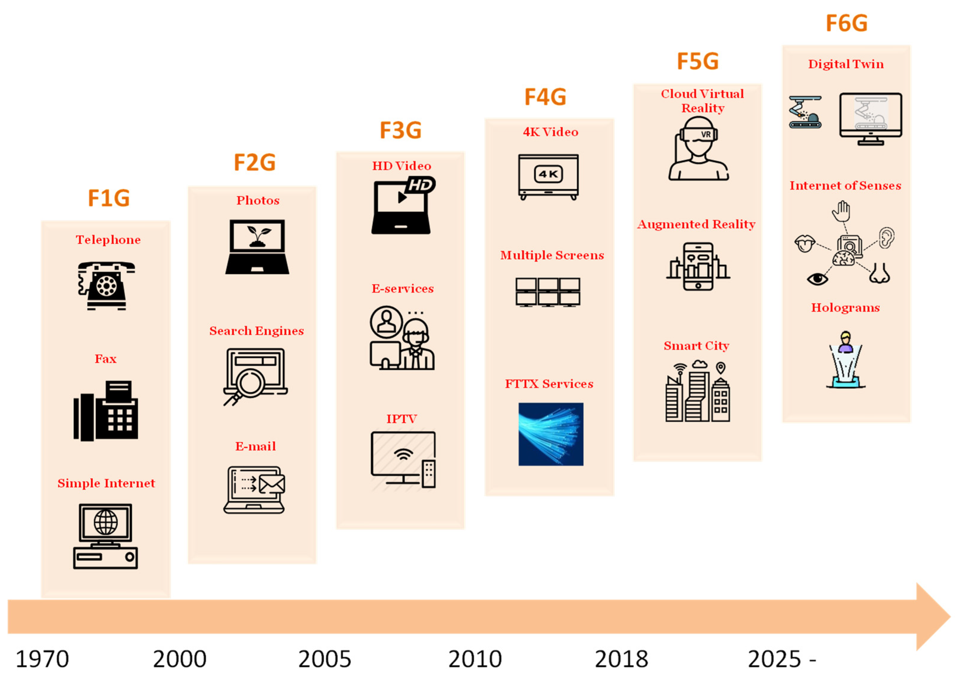
:1. Introduction
2. Services and Requirements for F6G
2.1. Classification of Services
2.2. Upcoming Categories of Services and Their Requirements
2.3. The Indispensable Network Transformation in Order to Realize the F6G Vision
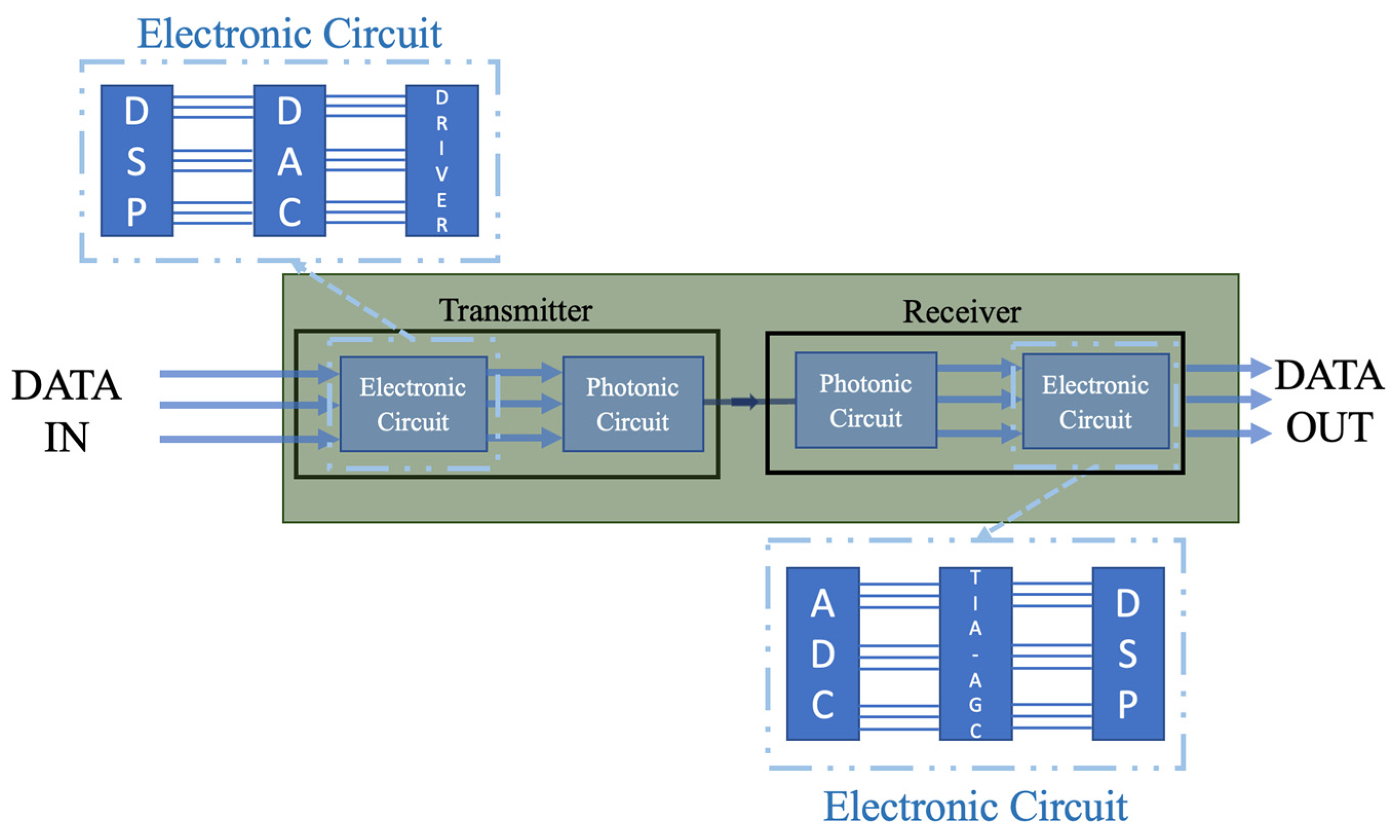
3. Photonics-Based Subsystems for All-Optical Processing
3.1. All-Optical Coherent and Simplified Coherent Solutions: Challenges and Opportunities


3.2. Photonic ADCs: Challenges and Opportunities
3.3. Photonic DACs: Challenges and Opportunities
3.4. Reconfigurable Photonics
4. Optical Transmission: Key Challenges and Proposed Directions
4.1. Capacity Scaling: What to Expect in the F6G


| Type | Modulation Format | Baud Rate | Channel Spacing | Data Rate | Required OSNIR (for BER = 10−3) |
|---|---|---|---|---|---|
| 100G | PM-QPSK | 32 Gbaud | 37.5 GHz | 100 Gb/s | 9.8 dB |
| 200G | PM-16QAM | 32 Gbaud | 37.5 GHz | 200 Gb/s | 16.55 dB |
| 400G | PM-16QAM | 63 Gbaud | 75 GHz | 400 Gb/s | 16.55 dB |
| PM-64QAM | 42 Gbaud | 50 GHz | 400 Gb/s | 22.5 dB | |
| PCS-16QAM | 80–95 Gbaud | 100 GHz | 400 Gb/s | varies | |
| 800G | PM-16QAM | 128 Gbaud | 150 GHz | 800 Gb/s | 16.55 dB |
| PM-32QAM | 96 Gbaud | 112.5 GHz | 800 Gb/s | 19.5 dB | |
| PM-64QAM | 80 Gbaud | 100 GHz | 800 Gb/s | 22.5 dB | |
| PCS-64QAM | 90 Gbaud | 100 GHz | 800 Gb/s | N/A | |
| 200–800G | Probabilistic Shaping | 60–95 Gbaud | 75–100 GHz | 200–800 Gb/s | varies |
4.2. Capacity Increase Using More Spectrally Efficient Modulation Formats
4.3. Capacity Increase Employing a Greater Number of Channels
4.3.1. Ultra-Wideband Transmission
Hollow-Core Fibers for Further Increasing the Transmission Spectrum
4.3.2. Space Division Multiplexing
- Multiplication of the number of conventional fibers (thus implementing parallelism that consists of single-core/single-mode fibers), considering the existence of at least one element that performs spatial integration, e.g., an amplifier with sharing pumps, a switching node, or terminal equipment, named bundles of Single-Mode Fibers (Bu-SMFs).
- Multiplication of the number of cores; within the fiber, multiple cores arranged within the cladding with each supporting a single spatial mode (Multi-Core Fiber—MCF), or multiple cores each supporting multiple modes (Multi-Core-Mode Fiber—MCMF). Coupled Core (CC) fibers. CC can provide strong mode coupling between the different cores, attaining shorter core-to-core distances and higher spatial density compared with the uncoupled MCFs.
- Multiplication of the number of modes in MMF fibers within a single core, supporting a discrete number of spatial modes (Multi-Mode Fiber—MMF, Few-Mode Fiber—FMF).
- A combination of the above categories, e.g., MCF/FMF, is also feasible.
SDM in Terrestrial and Submarine Networks
SDM in Wireless Fronthaul/Backhaul
SDM in Inter/Intra Data Center Networks
4.3.3. Summarizing the Benefits of UWB and SDM-Based Systems
4.3.4. Combining the Benefits of UWB and SDM
4.3.5. Towards the Ultimate Capacity Limits of Optical Transmission
Predictions on the Attainable Capacity
5. Optical Switching: Key Challenges and Proposed Directions
5.1. Need for More Sophisticated Switches to Support the F6G Ecosystem
- Reliable and low latency communication with guaranteed service quality for the digital transformation of industrial processes.
- Reduced congestion in data communication when a multiplicity of applications competes for simultaneous delivery, thereby causing data loss or a delay in data delivery.
- Reduced power consumption to some pico-Joule per bit through the broader use of optical networking technologies, interconnects, and integrated optical communication components.
- Lowered barrier for the uptake of higher-performance communication technologies by reducing the cost of transmission interfaces to around 50 cents per Gigabit per second.
5.2. Ultra-High Capacity Switching
5.2.1. On the Road towards Realizing a WBSS
5.2.2. Optical Node Switching Architectures
5.3. Ultra-Fast Switching
- (a)
- Offer seamless optical connectivity between factory buildings, micro-data centers, or edge cloud computing.
- (b)
- Ensure low congestion, latency, and jitter when routing the traffic flows in the optical domain from the various end-points of the industrial network.
- (c)
- Provide high scalability and cascadeability, allowing the seamless operation of a highly densified industrial environment, consisting of a large number of inter-connected “things” such as robots, machines, etc.
- (d)
- Provide a sufficient physical layer performance even for demanding industrial environments, which comprise a large number of inter-connected buildings and “things”, such as robots, machines, etc., ensuring a very low BER even after a large number of traversed nodes in a densified environment.
- (e)
- Provide a cost- and energy-efficient switching solution, which comprises low-cost and zero/low-power consumption components (e.g., power splitters, combiners, arrayed waveguide gratings, and wavelength blockers).
6. Conclusions
Author Contributions
Funding
Data Availability Statement
Conflicts of Interest
References
- Wild, T.; Braun, V.; Viswanathan, H. Joint Design of Communication and Sensing for Beyond 5G and 6G Systems. IEEE Access 2021, 9, 30845–30857. [Google Scholar] [CrossRef]
- Stavdas, A. 5G as a Catalyst for a Wider Technological Fusion that Enables the Fourth Industrial Revolution. In Proceedings of the IET Conference Proceedings, Online, 2–3 June 2021; pp. 39–49. [Google Scholar] [CrossRef]
- Stavdas, A. Networked Intelligence: A Wider Fusion of Technologies that Spurs the Fourth Industrial Revolution. Part II: The Transformation of Production Systems. World Rev. Political Econ. 2021, 12, 236–254. [Google Scholar] [CrossRef]
- Stavdas, A. Networked Intelligence: A Wider Fusion of Technologies that Spurs the Fourth Industrial Revolution. Part I: Foundations. World Rev. Political Econ. 2021, 12, 220–235. [Google Scholar] [CrossRef]
- Uzunidis, D.; Logothetis, M.; Stavdas, A.; Hillerkuss, D.; Tomkos, I. Fifty Years of Fixed Optical Networks Evolution: A Survey of Architectural and Technological Developments in a Layered Approach. Telecom 2022, 3, 619–674. [Google Scholar] [CrossRef]
- European Technology Platform NetWorld2020. Smart Networks in the context of NGI. Strategic Research and Innovation Agenda. Eur. Technol. Platf. 2021, 27, 1–240. [Google Scholar]
- Fifth Generation Fixed Network (F5G); F5G Generation Definition Release #1. Available online: https://www.etsi.org/technologies/fifth-generation-fixed-network-f5g (accessed on 8 October 2023).
- The Fifth Generation Fixed Network (F5G): Bringing Fiber to Everywhere and Everything; ETSI White Paper No. #41; ETSI: Valbonne, France, 2020; Available online: https://www.etsi.org/images/files/ETSIWhitePapers/etsi_wp_41_FSG_ed1.pdf (accessed on 8 October 2023).
- Jiang, W.; Han, B.; Habibi, M.A.; Schotten, H.D. The Road Towards 6G: A Comprehensive Survey. IEEE Open J. Commun. Soc. 2021, 2, 334–366. [Google Scholar] [CrossRef]
- Calabretta, N.; Prifti, K.; Tessema, N.; Xue, X.; Pan, B.; Stabile, R. Photonic Integrated WDM Cross-Connects for Optical Metro and Data Center Networks. Metro and Data Center Optical Networks and Short-Reach Links II; International Society for Optics and Photonics: Washington, DC, USA, 2019; Volume 10946, Available online: https://www.researchgate.net/publication/330813789_Photonic_integrated_WDM_cross-connects_for_optical_metro_and_data_center_networks (accessed on 8 October 2023).
- Pointurier, Y.; Benzaoui, N.; Lautenschlaeger, W.; Dembeck, L. End-to-End Time-Sensitive Optical Networking: Challenges and Solutions. J. Light. Technol. 2019, 37, 1732–1741. [Google Scholar] [CrossRef]
- Benzaoui, N.; Gonzalez, M.S.; Estaran, J.M.; Mardoyan, H.; Lautenschlaeger, W.; Gebhard, U.; Dembeck, L.; Bigo, S.; Pointurier, Y. Deterministic Dynamic Networks (DDN). J. Light. Technol. 2019, 37, 3465–3474. [Google Scholar] [CrossRef]
- Bigo, S.; Benzaoui, N.; Christodoulopoulos, K.; Miller, R.; Lautenschlaeger, W.; Frick, F. Dynamic Deterministic Digital Infrastructure for Time-Sensitive Applications in Factory Floors. IEEE J. Sel. Top. Quantum Electron. 2021, 27, 6000314. [Google Scholar] [CrossRef]
- Richardson, D.J. New optical fibers for high-capacity optical communications. Philos. Trans. R. Soc. A Math. Phys. Eng. Sci. 2016, 374, 20140441. [Google Scholar] [CrossRef]
- Saridis, G.M.; Alexandropoulos, D.; Zervas, G.; Simeonidou, D. Survey and Evaluation of Space Division Multiplexing: From Technologies to Optical Networks. IEEE Commun. Surv. Tutor. 2015, 17, 2136–2156. [Google Scholar] [CrossRef]
- Papapavlou, C.; Paximadis, K.; Uzunidis, D.; Tomkos, I. Toward SDM-Based Submarine Optical Networks: A Review of Their Evolution and Upcoming Trends. Telecom 2022, 3, 234–280. [Google Scholar] [CrossRef]
- Ji, P.N.; Qian, D.; Kanonakis, K.; Kachris, C.; Tomkos, I. Design and Evaluation of a Flexible-Bandwidth OFDM-Based Intra-Data Center Interconnect. IEEE J. Sel. Top. Quantum Electron. 2013, 19, 3700310. [Google Scholar] [CrossRef]
- Marom, D.M.; Colbourne, P.D.; D’Errico, A.; Fontaine, N.K.; Ikuma, Y.; Proietti, R.; Zong, L.; Rivas-Moscoso, J.M.; Tomkos, I. Survey of Photonic Switching Architectures and Technologies in Support of Spatially and Spectrally Flexible Optical Networking. J. Opt. Commun. Netw. 2017, 9, 1–26. [Google Scholar] [CrossRef]
- Rechtman, L.; Marom, D.M. Rectangular versus circular fiber core designs: New opportunities for mode division multiplexing? In Proceedings of the 2017 Optical Fiber Communications Conference and Exhibition (OFC), Anaheim, CA, USA, 17–21 March 2017; pp. 1–3. [Google Scholar]
- Jinno, M. Spatial Channel Network (SCN): Opportunities and Challenges of Introducing Spatial Bypass Toward the Massive SDM Era [Invited]. J. Opt. Commun. Netw. 2019, 11, 1–14. [Google Scholar] [CrossRef]
- Jones, N. The information factories. Nature 2018, 561, 163–166. [Google Scholar] [CrossRef]
- Nazarathy, M.; Tomkos, I. Accurate Power-Efficient Format- Scalable Multi-Parallel Optical Digital-to-Analogue Conversion. Photonics 2021, 8, 38. [Google Scholar] [CrossRef]
- Yariv, A. Dynamic analysis of the semiconductor laser as a current-controlled oscillator in the optical phased-lock loop: Applications. Opt. Lett. 2006, 30, 2191. [Google Scholar] [CrossRef]
- Doerr, C. Silicon-Photonic Integrated Circuits with Enhanced Optical Functionality for Data-Center Applications. In Proceedings of the Optical Fiber Communication Conference (OFC), San Diego, CA, USA, 28 March 2023. [Google Scholar]
- Nespola, A.; Franco, G.; Forghieri, F.; Traverso, M.; Anderson, S.; Webster, M.; Gaudino, R. Proof of Concept of Polarization-Multiplexed PAM Using a Compact Si-Ph Device. IEEE Photon. Technol. Lett. 2019, 31, 62–65. [Google Scholar] [CrossRef]
- Tomkos, I.; Tolmachev, A.; Agmon, A.; Meltsin, M.; Nikas, T.; Nazarathy, M. Low-Cost/Power Coherent Transceivers for Intra-Datacenter Interconnections and 5G Fronthaul Links. In Proceedings of the 2019 21st International Conference on Transparent Optical Networks (ICTON), Angers, France, 9–13 July 2019; pp. 1–5. [Google Scholar] [CrossRef]
- Morsy-Osman, M.; Sowailem, M.; El-Fiky, E.; Goodwill, T.; Hoang, T.; Lessard, S.; Plant, D.V. DSP-free ‘coherent-lite’ transceiver for next generation single wavelength optical intra-datacenter interconnects. Opt. Express 2018, 26, 8890–8903. [Google Scholar] [CrossRef]
- Doerr, C.R.; Chen, L. Monolithic PDM-DQPSK receiver in silicon. In Proceedings of the 36th European Conference and Exhibition on Optical Communication, Turin, Italy, 19–23 September 2010. [Google Scholar]
- Perin, J.K.; Shastri, A.; Kahn, J.M. Design of Low-Power DSP-Free Coherent Receivers for Data Center Links. J. Light. Technol. 2017, 35, 4650–4662. [Google Scholar] [CrossRef]
- Erkılınc, M.S.; Lavery, D.; Thomsen, B.C.; Killey, R.I.; Bayvel, P.; Savory, S.J. Polarization-insensitive single-balanced photodiode coherent receiver for long-reach WDM-PONs. J. Lightw. Technol. 2016, 34, 2034–2041. [Google Scholar] [CrossRef]
- Cano, I.N.; Lerin, A.; Polo, V.; Prat, J. Polarization independent single-PD coherent ONU receiver with centralized scrambling in WDM PONs. In Proceedings of the 2014 The European Conference on Optical Communication (ECOC), Cannes, France, 21–25 September 2014; pp. 1–3. [Google Scholar]
- Kazovsky, L.; Meissner, P.; Patzak, E. ASK multiport optical homodyne receivers. J. Light. Technol. 1987, 5, 770–791. [Google Scholar] [CrossRef]
- Zhou, J.; Caponio, N. Operative characteristics and application aspects of synchronous intra-bit polarization spreading for polarization independent heterodyne detection. IEEE Photon. Technol. Lett. 1994, 6, 295–298. [Google Scholar] [CrossRef]
- Ciaramella, E. Polarization-Independent Receivers for Low-Cost Coherent OOK Systems. IEEE Photon. Technol. Lett. 2014, 26, 548–551. [Google Scholar] [CrossRef]
- Altabas, J.A.; Silva Valdecasa, G.; Didriksen, M.; Lazaro, J.A.; Garces, I.; Tafur Monroy, I.; Jensen, J.B. Real-time 10Gbps Polarization Independent Quasicoherent Receiver for NG-PON2 Access Networks. In Proceedings of the 2018 Optical Fiber Communications Conference and Exposition: OFC, Los Angeles, CA, USA, 19 March–23 March 2018; pp. 1–3. [Google Scholar]
- Thomas, V.A.; Varughese, S.; Ralph, S.E. Quasicoherent Receivers for Access Networks Using Fullwave Rectification Based Envelope Detection. In Proceedings of the 2019 Conference on Lasers and Electro-Optics (CLEO), San Jose, CA, USA, 5–10 May 2019; pp. 1–2. [Google Scholar]
- Murmann, B. ADC Performance Survey 1997–2021. Available online: http://web.stanford.edu/~murmann/adcsurvey.html (accessed on 8 October 2023).
- Siegman, A.; Kuizenga, D. Proposed method for measuring picosecond pulsewidths and pulse shapes in CW mode-locked lasers. IEEE J. Quantum Electron. 1970, 6, 212–215. [Google Scholar] [CrossRef]
- Valley, G.C. Photonic analog-to-digital converters. Opt. Express 2007, 15, 1955–1982. [Google Scholar] [CrossRef]
- Khilo, A.; Spector, S.J.; Grein, M.E.; Nejadmalayeri, A.H.; Holzwarth, C.W.; Sander, M.Y.; Dahlem, M.S.; Peng, M.Y.; Geis, M.W.; DiLello, N.A.; et al. Photonic ADC: Overcoming the bottleneck of electronic jitter. Opt. Express 2012, 20, 4454–4469. [Google Scholar]
- Yariv, A.; Koumans, R. Time interleaved optical sampling for ultra-high speed A/D conversion. Electron. Lett. 1998, 34, 2012–2013. [Google Scholar]
- Krueger, B.; Makon, R.E.; Landolt, O.; Hidri, O.; Schweiger, T.; Krune, E.; Knoll, D.; Lischke, S.; Schulze, J. A monolithically integrated, optically clocked 10 GS/s sampler with a bandwidth of >30 GHz and a jitter of <30 fs in photonic SiGe BiCMOS technology. In Proceedings of the 2017 IEEE Custom Integrated Circuits Conference (CICC), Austin, TX, USA, 30 April–3 May 2017. [Google Scholar]
- Zazzi, A.; Müller, J.; Weizel, M.; Koch, J.; Fang, D.; Moscoso-Mártir, A.; Mashayekh, A.T.; Das, A.D.; Drayß, D.; Merget, F.; et al. Optically Enabled ADCs and Application to Optical Communications. IEEE Open J. Solid-State Circuits Soc. 2021, 1, 209–221. [Google Scholar] [CrossRef]
- Nazarathy, M.; Shaham, O. Spatially distributed successive approximation register (SDSAR) photonic ADCs based on phase-domain quantization. Opt. Express 2012, 20, 7833–7869. [Google Scholar] [CrossRef]
- Lopez, I.G.; Aimone, A.; Alreesh, S.; Rito, P.; Brast, T.; Hohns, V.; Fiol, G.; Gruner, M.; Fischer, J.K.; Honecker, J.; et al. DAC-Free Ultralow-Power Dual-Polarization 64-QAM Transmission at 32 GBd With Hybrid InP IQ SEMZM and BiCMOS Drivers Module. J. Light. Technol. 2017, 35, 404–410. [Google Scholar]
- Schell, M.; Fiol, G.; Aimone, A. DAC-free Generation of M-QAM Signals with InP Segmented Mach-Zehnder Modulators. In Proceedings of the 2017 Optical Fiber Communications Conference and Exhibition OFC, Los Angeles, CA, USA, 19–23 March 2017. [Google Scholar]
- Patel, D.; Samani, A.; Veerasubramanian, V.; Ghosh, S.; Plant, D.V. Silicon Photonic Segmented Modulator-Based Electro-Optic DAC for 100 Gb/s PAM-4 Generation. IEEE Photon. Technol. Lett. 2015, 27, 2433–2436. [Google Scholar]
- Sobu, Y.; Huang, G.; Tanaka, S.; Tanaka, Y.; Akiyama, Y.; Hoshida, T. High-Speed Optical Digital-to-Analog Converter Operation of Compact Two-Segment All-Silicon Mach–Zehnder Modulator. J. Light. Technol. 2020, 39, 1148–1154. [Google Scholar] [CrossRef]
- Vanhoecke, M.; Argyris, N.; Aimone, A.; Dris, S.; Apostolopoulos, D.; Verheyen, K.; Vaernewyck, R.; Torfs, G.; Yin, X.; Bosman, E.; et al. Multi-level optical signal generation using a segmented-electrode InP IQ-MZM with integrated CMOS binary drivers. In Proceedings of the 42nd European Conference on Optical Communication, ECOC, Dusseldorf, Germany, 18–22 September 2016; pp. 352–354. [Google Scholar]
- Aimone, A.; Lopez, I.G.; Alreesh, S.; Rito, P.; Brast, T.; Höhns, V.; Fiol, G.; Gruner, M.; Fischer, J.K.; Honecker, J.; et al. DAC-free ultra-low-power dual-polarization 64-QAM transmission with InP IQ segmented MZM module. In Proceedings of the 2016 Optical Fiber Communications Conference and Exhibition (OFC), Anaheim, CA, USA, 20–24 March 2016; pp. 1–3. [Google Scholar]
- Aimone, A.; Frey, F.; Elschner, R.; Lopez, I.G.; Fiol, G.; Rito, P.; Gruner, M.; Ulusoy, A.C.; Kissinger, D.; Fischer, J.K.; et al. DAC-Less 32-GBd PDM-256-QAM Using Low-Power InP IQ Segmented MZM. IEEE Photon. Technol. Lett. 2017, 29, 221–223. [Google Scholar]
- Ehrlichman, Y.; Amrani, O.; Ruschin, S. Improved Digital-to-Analog Conversion Using Multi-Electrode Mach–Zehnder Interfer-ometer. J. Light. Technol. 2008, 26, 3567–3575. [Google Scholar]
- Giuglea, A.; Belfiore, G.; Khafaji, M.; Henker, R.; Petousi, D.; Winzer, G.; Zimmermann, L.; Ellinger, F. Comparison of Segmented and Traveling-Wave Electro-Optical Transmitters Based on Silicon Photonics Mach-Zehnder Modulators. In Proceedings of the 2018 Photonics in Switching and Computing, PSC 2018, Limassol, Cyprus, 19–21 September 2018; pp. 2018–2020. [Google Scholar]
- Verbist, J.; Verplaetse, M.; Lambrecht, J.; Srivinasan, S.A.; de Heyn, P.; de Keulenaer, T.; Pierco, R.; Vyncke, A.; Absil, P.; Yin, X.; et al. 100 Gb/s DAC-less and DSP-free transmitters using GeSi EAMs for short-reach optical interconnects. In Proceedings of the 2018 Optical Fiber Communications Conference and Exposition, OFC 2018-Proceedings, San Diego, CA, USA, 11–15 March 2018; pp. 1–3. [Google Scholar]
- Yamazaki, H.; Yamada, T.; Goh, T.; Mino, S. Multilevel optical modulator with PLC and LiNbO3 hybrid integrated circuit. In Proceedings of the OFC 2011, Los Angeles, CA, USA, 6–10 March 2011. [Google Scholar]
- Sano, A.; Kobayashi, T.; Ishihara, K.; Masuda, H.; Yamamoto, S.; Mori, K.; Yamazaki, E.; Yoshida, E.; Miyamoto, Y.; Yamada, T.; et al. 240-Gb/s polarization-multiplexed 64-QAM modulation and blind detection using PLC-LN hybrid integrated modulator and digital coherent receiver. In Proceedings of the European Conference on Optical Communication, Vienna, Austria, 20–24 September 2009; Volume 2009. [Google Scholar]
- Yamazaki, H.; Yamada, T.; Goh, T.; Kaneko, A. PDM-QPSK modulator with a hybrid configuration of silica PLCs and LiNbO3 phase modulators. J. Light. Technol. 2011, 29, 721–727. [Google Scholar] [CrossRef]
- Yamazaki, H.; Yamada, T.; Goh, T.; Kaneko, A. 64QAM Modulator with a Hybrid Configuration of Silica PLCs and LiNbO3 Phase Modulators for 100-Gb/s Applications Hiroshi. In Proceedings of the ECOC 2009, Vienna, Austria, 20–24 September 2009; pp. 1–4. [Google Scholar]
- Nazarathy, M.; Tomkos, I. Energy-Efficient Reconfigurable 4|16|64|256-QAM Transmitter Based on PAM2|4-Driven Optical DACs. IEEE Photon. Technol. Lett. 2022, 34, 1159–1162. [Google Scholar]
- Bogaerts, W.; Pérez, D.; Capmany, J.; Miller, D.A.B.; Poon, J.; Englund, D.; Morichetti, F.; Melloni, A. Programmable photonic circuits. Nature 2020, 586, 207–216. [Google Scholar]
- Pérez, D.; Gasulla, I.; Crudgington, L.; Thomson, D.J.; Khokhar, A.Z.; Li, K.; Cao, W.; Mashanovich, G.Z.; Capmany, J. Multipurpose silicon photonics signal processor core. Nat. Commun. 2017, 8, 636. [Google Scholar]
- Perez, D.; Gasulla, I.; Capmany, J. Reconfigurable integrated waveguide meshes for photonic signal processing and emerging applications. Integr. Opt. Devices Mater. Technol. XXII 2018, 10535, 197–209. [Google Scholar]
- Ellis, A.D.; Mac Suibhne, N.; Saad, D.; Payne, D.N. Communication networks beyond the capacity crunch. Philos. Trans. R. Soc. A Math. Phys. Eng. Sci. 2016, 374, 20150191. [Google Scholar] [CrossRef] [PubMed]
- Karanov, B.; Chagnon, M.; Thouin, F.; Eriksson, T.A.; Bulow, H.; Lavery, D.; Bayvel, P.; Schmalen, L. End-to-End Deep Learning of Optical Fiber Communications. J. Light. Technol. 2018, 36, 4843–4855. [Google Scholar] [CrossRef]
- Essiambre, R.-J.; Kramer, G.; Winzer, P.J.; Foschini, G.J.; Goebel, B. Capacity Limits of Optical Fiber Networks. J. Light. Technol. 2010, 28, 662–701. [Google Scholar] [CrossRef]
- Winzer, P.J.; Neilson, D.T. From Scaling Disparities to Integrated Parallelism: A Decathlon for a Decade. J. Light. Technol. 2017, 35, 1099–1115. [Google Scholar] [CrossRef]
- Winzer, P.J.; Neilson, D.T.; Chraplyvy, A.R. Fiber-optic transmission and networking: The previous 20 and the next 20 years. Opt. Express 2018, 26, 24190–24239. [Google Scholar] [CrossRef]
- Aguiar, R.L.; Bourse, D.; Hecker, A.; Huusko, J.; Pouttu, A. Strategic Research and Innovation Agenda 2022. NetworldEurope; Zenodo: Honolulu, HI, USA, 2022. [Google Scholar] [CrossRef]
- Nagatani, M.; Wakita, H.; Yamazaki, H.; Ogiso, Y.; Mutoh, M.; Ida, M.; Hamaoka, F.; Nakamura, M.; Kobayashi, T.; Miyamoto, Y.; et al. A Beyond-1-Tb/s Coherent Optical Transmitter Front-End Based on 110-GHz-Bandwidth 2:1 Analog Multiplexer in 250-nm InP DHBT. IEEE J. Solid State Circuits 2020, 55, 2301–2315. [Google Scholar] [CrossRef]
- Eppenberger, M.; Bitachon, B.I.; Messner, A.; Heni, W.; Habegger, P.; Destraz, M.; De Leo, E.; Meier, N.; Del Medico, N.; Hoessbacher, C.; et al. Plasmonic Racetrack Modulator Transmitting 220 Gbit/s OOK and 408 Gbit/s 8PAM. In Proceedings of the 2021 European Conference on Optical Communication (ECOC), Bordeaux, France, 13–16 September 2021. [Google Scholar]
- Pittalà, F.; Braun, R.-P.; Boecherer, G.; Schulte, P.; Schaedler, M.; Bettelli, S.; Calabrò, S.; Kuschnerov, M.; Gladisch, A.; Westphal, F.-J.; et al. Single-Carrier Coherent 930G, 1.28T and 1.60T Field Trial. In Proceedings of the 2021 European Conference on Optical Communication (ECOC), Bordeaux, France, 13–16 September 2021. [Google Scholar]
- Xiang, L. Evolution of Fiber-Optic Transmission and Networking toward the 5G Era. iScience 2019, 22, 489–506. [Google Scholar]
- Agrell, E.; Karlsson, M.; Chraplyvy, A.R.; Richardson, D.J.; Krummrich, P.M.; Winzer, P.; Roberts, K.; Fischer, J.K.; Savory, S.J.; Eggleton, B.J.; et al. Roadmap of optical communications. J. Opt. 2016, 18, 063002. [Google Scholar] [CrossRef]
- Uzunidis, D.; Apostolopoulou, F.; Pagiatakis, G.; Stavdas, A. Analysis of Available Components and Performance Estimation of Optical Multi-Band Systems. Eng 2021, 2, 531–543. [Google Scholar] [CrossRef]
- Knittle, C. IEEE 50 Gb/s EPON (50G-EPON). In Proceedings of the 2020 Optical Fiber Communications Conference and Exhibition (OFC), San Diego, CA, USA, 8–12 March 2020; pp. 1–3. [Google Scholar]
- ENA. 100G PON; XENA Networks, White Paper; ENA: Schaumburg, IL, USA, 2017. [Google Scholar]
- Available online: https://www.zte.com.cn/global/about/magazine/zte-technologies/2017/5/en_734/465612.html (accessed on 8 October 2023).
- Available online: https://www.telcotitans.com/vodafonewatch/vodafone-tests-100g-pon-waters-with-nokia/2990.article (accessed on 8 October 2023).
- Shaddad, R.; Mohammad, A.; Al-Gailani, S.; Al-Hetar, A.; Elmagzoub, M. A survey on access technologies for broadband optical and wireless networks. J. Netw. Comput. Appl. 2014, 41, 459–472. [Google Scholar] [CrossRef]
- Horvath, T.; Munster, P.; Oujezsky, V.; Bao, N.-H. Passive Optical Networks Progress: A Tutorial. Electronics 2020, 9, 1081. [Google Scholar] [CrossRef]
- Kanonakis, K.; Cvijetic, N.; Tomkos, I.; Wang, T. Dynamic Software-Defined Resource Optimization in Next-Generation Optical Access Enabled by OFDMA-Based Meta-MAC Provisioning. J. Light. Technol. 2013, 31, 2296–2306. [Google Scholar] [CrossRef]
- Reis, J.D.; Ferreira, R.M.; Rossi, S.M.; Suzigan, G.J.; Pinto, T.M.S.; Shahpari, A.; Teixeira, A.L.; Gonzalez, N.G.; Oliveira, J.R.F. Bidirectional coherent WDM-PON performance with real-time Nyquist 16QAM transmitter. In Proceedings of the 2015 Optical Fiber Communications Conference and Exhibition (OFC), Los Angeles, CA, USA, 22–26 March 2015. [Google Scholar]
- Available online: https://www.infinera.com/innovation/xr-optics (accessed on 8 October 2023).
- Xu, Z.; Tan, Z.; Yang, C. Research on Performances of Coherent Nyquist-WDM-PON and WDM-OFDM-PON Using Effective Phase Noise Suppression Methods. In Proceedings of the 2016 Asia Communications and Photonics Conference (ACP), Wuhan, China, 2–5 November 2016. [Google Scholar]
- Fehenberger, T.; Alvarado, A.; Bocherer, G.; Hanik, N. On Probabilistic Shaping of Quadrature Amplitude Modulation for the Nonlinear Fiber Channel. J. Light. Technol. 2016, 34, 5063–5073. [Google Scholar] [CrossRef]
- Cho, J.; Winzer, P.J. Probabilistic Constellation Shaping for Optical Fiber Communications. J. Light. Technol. 2019, 37, 1590–1607. [Google Scholar] [CrossRef]
- Poggiolini, P.; Nespola, A.; Jiang, Y.; Bosco, G.; Carena, A.; Bertignono, L.; Bilal, S.M.; Abrate, S.; Forghieri, F. Analytical and Experimental Results on System Maximum Reach Increase Through Symbol Rate Optimization. J. Light. Technol. 2016, 34, 1872–1885. [Google Scholar] [CrossRef]
- Nikolaou, K.F.; Uzunidis, D.; Stavdas, A.; Pagiatakis, G. Quantifying the Impact of Physical Layer Effects in an Optical Multi-Band System. In Proceedings of the 29th Telecommunications forum TELFOR, Serbia, Belgrade, 23–24 November 2021. [Google Scholar]
- Uzunidis, D.; Matrakidis, C.; Stavdas, A.; Lord, A. Power Optimization Strategy for Multi-Band Optical Systems. In Proceedings of the European Conference of Optical Communications, ECOC’ 20, Brussels, Belgium, 6–10 December 2020. [Google Scholar]
- Uzunidis, D.; Kosmatos, E.; Matrakidis, C.; Stavdas, A.; Lord, A. Strategies for Upgrading an Operator’s Backbone Network Beyond the C-Band: Towards Multi-Band Optical Networks. IEEE Photon. J. 2021, 13, 1–18. [Google Scholar] [CrossRef]
- Uzunidis, D.; Matrakidis, C.; Kosmatos, E.; Stavdas, A.; Petropoulos, P.; Lord, A. Connectivity Challenges in E, S, C and L Optical Multi-Band Systems. In Proceedings of the 2021 European Conference on Optical Communication (ECOC), Bordeaux, France, 13–16 September 2021; pp. 1–4. [Google Scholar]
- Sano, A.; Masuda, H.; Kobayashi, T.; Fujiwara, M.; Horikoshi, K.; Yoshida, E.; Miyamoto, Y.; Matsui, M.; Mizoguchi, M.; Yamazaki, H.; et al. 69.1-Tb/s (432 × 171-Gb/s) C- and extended L-band transmission over 240 km Using PDM-16-QAM modulation and digital coherent detection. In Proceedings of the 2010 Conference on Optical Fiber Communication (OFC/NFOEC), Collocated National Fiber Optic Engineers Conference, San Diego, CA, USA, 21–25 March 2010; pp. 1–3. [Google Scholar]
- Qian, D.; Huang, M.-F.; Ip, E.; Huang, Y.-K.; Shao, Y.; Hu, J.; Wang, T. 101.7-Tb/s (370 × 294-Gb/s) PDM-128QAM-OFDM transmission over 3 × 55-km SSMF using pilot-based phase noise mitigation. In Proceedings of the 2011 Optical Fiber Communication Conference and Exposition and the National Fiber Optic Engineers Conference, Los Angeles, CA, USA, 6–10 March 2011; pp. 1–3. [Google Scholar]
- Kobayashi, T.; Yamanaka, S.; Matsuura, A.; Kawakami, H.; Miyamoto, Y.; Ishihara, K.; Masuda, H. 102.3-Tb/s (224 × 548-Gb/s) C- and extended L-band all-Raman transmission over 240 km using PDM-64QAM single carrier FDM with digital pilot tone. In Proceedings of the OFC/NFOEC, Los Angeles, CA, USA, 4–8 March 2012; pp. 1–3. [Google Scholar]
- Zhu, B.; Xie, C.; Nelson, L.E.; Jiang, X.; Peckham, D.; Lingle, R.; Yan, M.F.; Wisk, P.W.; DiGiovanni, D.J. 70 nm seamless band transmission of 17.3 Tb/s over 40 × 100 km of fiber using complementary Raman/EDFA. In Proceedings of the 2015 Optical Fiber Communications Conference and Exhibition (OFC), Los Angeles, CA, USA, 22–26 March 2015; pp. 1–3. [Google Scholar]
- Cai, J.-X.; Sun, Y.; Zhang, H.; Batshon, H.G.; Mazurczyk, M.V.; Sinkin, O.V.; Foursa, D.G.; Pilipetskii, A. 49.3 Tb/s Transmission Over 9100 km Using C + L EDFA and 54 Tb/s Transmission Over 9150 km Using Hybrid-Raman EDFA. J. Light. Technol. 2015, 33, 2724–2734. [Google Scholar] [CrossRef]
- Okamoto, S.; Horikoshi, K.; Hamaoka, F.; Minoguchi, K.; Hirano, A. 5-band (O, E, S, C, and L) WDM Transmission with Wavelength Adaptive Modulation Format Allocation. In Proceedings of the ECOC 2016, 42nd European Conference on Optical Communication, Dusseldorf, Germany, 18–22 September 2016; pp. 1–3. [Google Scholar]
- Saavedra, G.; Tan, M.; Elson, D.J.; Galdino, L.; Semrau, D.; Iqbal, A.; Phillips, I.D.; Harper, P.; Ellis, A.; Thomsen, B.C.; et al. Experimental Analysis of Nonlinear Impairments in Fibre Optic Transmission Systems up to 7.3 THz. J. Light. Technol. 2017, 35, 4809–4816. [Google Scholar] [CrossRef]
- Ghazisaeidi, A.; Ruiz, I.F.d.J.; Rios-Muller, R.; Schmalen, L.; Tran, P.; Brindel, P.; Meseguer, A.C.; Hu, Q.; Buchali, F.; Charlet, G.; et al. Advanced C + L-Band Transoceanic Transmission Systems Based on Probabilistically Shaped PDM-64QAM. J. Light. Technol. 2017, 35, 1291–1299. [Google Scholar] [CrossRef]
- Renaudier, J.; Meseguer, A.C.; Ghazisaeidi, A.; Tran, P.; Muller, R.R.; Brenot, R.; Verdier, A.; Blache, F.; Mekhazni, K.; Duval, B.; et al. First 100-nm Continuous-Band WDM Transmission System with 115Tb/s Transport over 100km Using Novel Ultra-Wideband Semiconductor Optical Amplifiers. In Proceedings of the 2017 European Conference on Optical Communication (ECOC), Gothenburg, Sweden, 17–21 September 2017; pp. 1–3. [Google Scholar]
- Cai, J.-X.; Batshon, H.G.; Mazurczyk, M.V.; Sinkin, O.V.; Wang, D.; Paskov, M.; Davidson, C.R.; Patterson, W.W.; Bolshtyansky, M.A.; Foursa, D.G. 51.5 Tb/s Capacity over 17,107 km in C + L Bandwidth Using Single Mode Fibers and Nonlinearity Compensation. In Proceedings of the 2017 European Conference on Optical Communication (ECOC), Gothenburg, Sweden, 17–21 September 2017; pp. 1–3. [Google Scholar]
- Cai, J.-X.; Batshon, H.G.; Mazurczyk, M.V.; Sinkin, O.V.; Wang, D.; Paskov, M.; Patterson, W.W.; Davidson, C.R.; Corbett, P.C.; Wolter, G.M.; et al. 70.46 Tb/s Over 7600 km and 71.65 Tb/s Over 6970 km Transmission in C + L Band Using Coded Modulation with Hybrid Constellation Shaping and Nonlinearity Compensation. J. Light. Technol. 2018, 36, 114–121. [Google Scholar] [CrossRef]
- Cai, J.-X.; Batshon, H.G.; Mazurczyk, M.V.; Davidson, C.R.; Sinkin, O.V.; Wang, D.; Paskov, M.; Patterson, W.W.; Bolshtyansky, M.A.; Foursa, D.G. 94.9 Tb/s Single Mode Capacity Demonstration over 1900 km with C + L EDFAs and Coded Modulation. In Proceedings of the 2018 European Conference on Optical Communication (ECOC), Rome, Italy, 23–27 September 2018; pp. 1–3. [Google Scholar]
- Ionescu, M.; Galdino, L.; Edwards, A.; James, J.; Pelouch, W.; Sillekens, E.; Semrau, D.; Lavery, D.; Killey, R.I.; Barnes, S.; et al. 91 nm C + L Hybrid Distributed Raman–Erbium-Doped Fibre Amplifier for High Capacity Subsea Transmission. In Proceedings of the 2018 European Conference on Optical Communication (ECOC), Rome, Italy, 23–27 September 2018; pp. 1–3. [Google Scholar]
- Galdino, L.; Edwards, A.; Ionescu, M.; James, J.; Pelouch, W.; Sillekens, E.; Semrau, D.; Lavery, D.; Killey, R.I.; Barnes, S.; et al. 120 Tbit/s Transmission over Single Mode Fibre using Continuous 91 nm Hybrid Raman-EDFA Amplification. arXiv 2018, arXiv:1804.01845. [Google Scholar]
- Hamaoka, F.; Minoguchi, K.; Sasai, T.; Matsushita, A.; Nakamura, M.; Okamoto, S.; Yamazaki, E.; Kisaka, Y. 150.3-Tb/s Ultra-Wideband (S, C, and L Bands) Single-Mode Fibre Transmission over 40-km Using >519Gb/s/A PDM-128QAM Signals. In Proceedings of the 2018 European Conference on Optical Communication (ECOC), Rome, Italy, 23–27 September 2018; pp. 1–3. [Google Scholar]
- Lopez, V.; Zhu, B.; Moniz, D.; Costa, N.; Pedro, J.; Xu, X.; Kumpera, A.; Dardis, L.; Rahn, J.; Sanders, S. Optimized Design and Challenges for C&L Band Optical Line Systems. J. Light. Technol. 2020, 38, 1080–1091. [Google Scholar]
- Ionescu, M.; Lavery, D.; Edwards, A.; Sillekens, E.; Galdino, L.; Semrau, D.; Killey, R.I.; Pelouch, W.; Barnes, S.; Bayvel, P. 74.38 Tb/s Transmission Over 6300 km Single Mode Fiber with Hybrid EDFA/Raman Amplifiers. In Proceedings of the 2019 Optical Fiber Communications Conference and Exhibition (OFC), San Diego, CA, USA, 3–7 March 2019; pp. 1–3. [Google Scholar]
- Hamaoka, F.; Nakamura, M.; Okamoto, S.; Minoguchi, K.; Sasai, T.; Matsushita, A.; Yamazaki, E.; Kisaka, Y. Ultra-Wideband WDM Transmission in S-, C-, and L-Bands Using Signal Power Optimization Scheme. J. Light. Technol. 2019, 37, 1764–1771. [Google Scholar] [CrossRef]
- Iqbal, A.; Di Rosa, G.; Krzczanowicz, L.; Phillips, I.; Harper, P.; Richter, A.; Forysiak, W. Impact of pump-signal overlap in S + C + L band discrete Raman amplifiers. Opt. Express 2020, 28, 18440–18448. [Google Scholar] [CrossRef]
- Kato, T.; Watanabe, S.; Yamauchi, T.; Nakagawa, G.; Muranaka, H.; Tanaka, Y.; Akiyama, Y.; Hoshida, T. Real-time transmission of 240 × 200-Gb/s signal in S + C + L triple-band WDM without S- or L-band transceivers. In Proceedings of the 45th European Conference on Optical Communication (ECOC 2019), Dublin, Ireland, 22–26 September 2019; pp. 1–4. [Google Scholar]
- Arnould, A.; Ryf, R.; Chen, H.; Achouche, M.; Renaudier, J.; Ghazisaeidi, A.; Le Gac, D.; Brindel, P.; Makhsiyan, M.; Mekhazni, K.; et al. 103 nm Ultra-Wideband Hybrid Raman/SOA Transmission Over 3 × 100 km SSMF. J. Light. Technol. 2020, 38, 504–508. [Google Scholar] [CrossRef]
- Renaudier, J.; Arnould, A.; Ghazisaeidi, A.; Le Gac, D.; Brindel, P.; Awwad, E.; Makhsiyan, M.; Mekhazni, K.; Blache, F.; Boutin, A.; et al. Recent Advances in 100+ nm Ultra-Wideband Fiber-Optic Transmission Systems Using Semiconductor Optical Amplifiers. J. Light. Technol. 2020, 38, 1071–1079. [Google Scholar] [CrossRef]
- Galdino, L.; Edwards, A.; Yi, W.; Sillekens, E.; Wakayama, Y.; Gerard, T.; Pelouch, W.S.; Barnes, S.; Tsuritani, T.; Killey, R.I.; et al. Optical Fibre Capacity Optimisation via Continuous Bandwidth Amplification and Geometric Shaping. IEEE Photon. Technol. Lett. 2020, 32, 1021–1024. [Google Scholar] [CrossRef]
- Le Gac, D.; Bendimerad, D.; Demirtzioglou, I.; De Jauregui Ruiz, I.F.; Lorences-Riesgo, A.; El Dahdah, N.; Gallet, A.; Elfaiki, H.; Yu, S.; Gao, G.; et al. 63.2Tb/s Real-time Transmission Through Discrete Extended C- and L-Band Amplification in a 440km SMF Link. In Proceedings of the 2021 European Conference on Optical Communication (ECOC), Bordeaux, France, 13–16 September 2021; pp. 1–4. [Google Scholar]
- Demirtzioglou, I.; Bendimerad, D.F.; de Jauregui Ruiz, I.F.; Le Gac, D.; Lorences-Riesgo, A.; El Dahdah, N.; Gallet, A.; Elfaiki, H.; Yu, S.; Gao, G.; et al. 107.6 Tb/s GMI Throughput over 220 km SSMF using Discrete C- and L-Band Amplification across >12 THz. In Proceedings of the 2021 Optical Fiber Communications Conference and Exhibition (OFC), San Francisco, CA, USA, 6–10 June 2021; pp. 1–3. [Google Scholar]
- Mizuno, T.; Shibahara, K.; Ye, F.; Sasaki, Y.; Amma, Y.; Takenaga, K.; Jung, Y.; Pulverer, K.; Ono, H.; Abe, Y.; et al. Long-Haul Dense Space-Division Multiplexed Transmission Over Low-Crosstalk Heterogeneous 32-Core Transmission Line Using a Partial Recirculating Loop System. J. Light. Technol. 2017, 35, 488–498. [Google Scholar] [CrossRef]
- Hayashi, T.; Tamura, Y.; Hasegawa, T.; Taru, T. Record-Low Spatial Mode Dispersion and Ultra-Low Loss Coupled Multi-Core Fiber for UltraLong-Haul Transmission. J. Light. Technol. 2017, 35, 450–457. [Google Scholar] [CrossRef]
- Milione, G.; Ip, E.; Li, M.-J.; Stone, J.; Peng, G.; Wang, T. Mode crosstalk matrix measurement of a 1 km elliptical core few-mode optical fiber. Opt. Lett. 2016, 41, 2755–2758. [Google Scholar] [CrossRef]
- Jain, S.; Castro, C.; Jung, Y.; Hayes, J.; Sandoghchi, R.; Mizuno, T.; Sasaki, Y.; Amma, Y.; Miyamoto, Y.; Bohn, M.; et al. 32-core erbium/ytterbium-doped multicore fiber amplifier for next generation space-division multiplexed transmission system. Opt. Express 2017, 25, 32887–32896. [Google Scholar] [CrossRef]
- Ip, E.; Li, M.J.; Bennett, K.; Huang, Y.K.; Tanaka, A.; Korolev, A.; Koreshkov, K.; Wood, W.; Mateo, E.; Hu, J.; et al. 146λ × 6 × 19-Gbaud wavelength-and mode division multiplexed transmission over 10 × 50-km spans of few-mode fiber with a gain-equalized few-mode EDFA. J. Light. Technol. 2013, 32, 790–797. [Google Scholar] [CrossRef]
- Gnauck, A.H.; Winzer, P.J.; Jopson, R.M.; Burrows, E.C. Efficient pumping scheme for amplifier arrays with shared pump laser. In Proceedings of the ECOC 2016; 42nd European Conference on Optical Communication, Dusseldorf, Germany, 18–22 September 2016. [Google Scholar]
- Du, J.; Zheng, L.; Xu, K.; Chen, G.; Ma, L.; Liu, Y.; He, Z. High speed and small footprint silicon micro-ring modulator assembly for space-division-multiplexed 100-Gbps optical interconnection. Opt. Express 2018, 26, 13721–13729. [Google Scholar] [CrossRef] [PubMed]
- Ferrari, A.; Napoli, A.; Fischer, J.K.; Costa, N.; D’Amico, A.; Pedro, J.; Forysiak, W.; Pincemin, E.; Lord, A.; Stavdas, A.; et al. Assessment on the achievable throughput of multi-band ITU-T G. 652. D fiber transmission systems. J. Light. Technol. 2020, 38, 4279–4291. [Google Scholar] [CrossRef]
- RaJana, K.; Mitra, A.; Pradhan, A.; Grattan, K.; Srivastava, A.; Mukherjee, B.; Lord, A. When Is Operation C + L Bands More Economical than Multifiber for Capacity Upgrade of an Optical Backbone Network? In Proceedings of the 2020 European Conference on Optical Communications (ECOC), Brussels, Belgium, 6–10 December 2020; IEEE: Piscataway, NJ, USA, 2020. [Google Scholar]
- Kobayashi, T.; Nakamura, M.; Hamaoka, F.; Shibahara, K.; Mizuno, T.; Sano, A.; Kawakami, H.; Isoda, A.; Nagatani, M.; Yamazaki, H.; et al. 1-Pb/s (32 SDM/46 WDM/768 Gb/s) C-band dense SDM transmission over 205.6-km of single-mode heterogeneous multi-core fiber using 96-Gbaud PDM-16QAM channels. In Proceedings of the 2017 Optical Fiber Communications Conference and Exhibition (OFC), Los Angeles, CA, USA, 19–23 March 2017; pp. 1–3. [Google Scholar]
- Pulverer, K.; Tanaka, T.; Häbel, U.; Castro, C.; Bohn, M.; Mizuno, T.; Isoda, A.; Shibahara, K.; Inui, T.; Miyamoto, Y.; et al. First Demonstration of Single-Mode MCF Transport Network with Crosstalk-Aware In-Service Optical Channel Control. In Proceedings of the 2017 European Conference on Optical Communication (ECOC), Gothenburg, Sweden, 17–21 September 2017; pp. 1–3. [Google Scholar] [CrossRef]
- Takasaka, S.; Maeda, K.; Kawasaki, K.; Yoshioka, K.; Oshio, H.; Sugizaki, R.; Kawaguchi, Y.; Takahashi, H.; Tsuritani, T.; Shiino, M. Increase of Cladding Pump Power Efficiency by a 19 Core Erbium Doped Fibre Amplifier. In Proceedings of the 2017 European Conference on Optical Communication (ECOC), Gothenburg, Sweden, 17–21 September 2017; pp. 1–3. [Google Scholar]
- Thouras, J.; Pincemin, E.; Amar, D.; Gravey, P.; Morvan, M.; Moulinard, M.-L. Introduction of 12 Cores Optical Amplifiers in Optical Transport Network: Performance Study and Economic Impact. In Proceedings of the 2018 20th International Conference on Transparent Optical Networks (ICTON), Bucharest, Romania, 1–5 July 2018; pp. 1–4. [Google Scholar]
- Jinno, M.; Kodama, T. Spatial Channel Network (SCN): Introducing Spatial Bypass Toward the SDM Era. In Proceedings of the Optical Fiber Communication Conference (OFC), San Diego, CA, USA, 8–12 March 2020; pp. 1–3. [Google Scholar]
- Luis, R.S.; Puttnam, B.J.; Rademacher, G.; Eriksson, T.A.; Hirota, Y.; Shinada, S.; Ross-Adams, A.; Gross, S.; Withford, M.; Maruyama, R.; et al. Demonstration of a 1 Pb/s spatial channel network node. In Proceedings of the 45th European Conference on Optical Communication (ECOC 2019), Dublin, Ireland, 22–26 September 2019; pp. 1–4. [Google Scholar]
- Marom, D.M.; Blau, M. Switching solutions for WDM-SDM optical networks. IEEE Commun. Mag. 2015, 53, 60–68. [Google Scholar] [CrossRef]
- Miyamoto, Y.; Suzuki, K.; Nakajima, K. Multicore fiber transmission system for high-capacity optical transport network. Next-Gener. Opt. Commun. Compon. Sub-Syst. Syst. VIII 2019, 10947, 1094703. [Google Scholar]
- Pecci, P.; Jovanovski, L.; Barezzani, M.; Kamalov, V.; Marcerou, J.F.; Cantono, M. Pump Farming as enabling factor to increase subsea cable. Proc. SubOptic. 2019, 2019, 1–7. [Google Scholar]
- Bolshtyansky, M.A.; Sinkin, O.V.; Paskov, M.; Hu, Y.; Cantono, M.; Jovanovski, L.; Pilipetskii, A.N.; Mohs, G.; Kamalov, V.; Vusirikala, V. Single-Mode Fiber SDM Submarine Systems. J. Light. Technol. 2019, 38, 1296–1304. [Google Scholar] [CrossRef]
- Papapavlou, C.; Paximadis, K.; Tzimas, G. Design and Analysis of a new SDM submarine optical network for Greece. In Proceedings of the 2021 12th International Conference on Information, Intelligence, Systems & Applications (IISA), Chania Crete, Greece, 12–14 July 2021. [Google Scholar]
- Lagkas, T.; Klonidis, D.; Sarigiannidis, P.; Tomkos, I. 5G/NGPON Evolution and Convergence: Developing on Spatial Multiplexing of Optical Fiber Links for 5G Infrastructures. Fiber Integr. Opt. 2020, 39, 4–23. [Google Scholar] [CrossRef]
- Desurvire, E.B. Capacity Demand and Technology Challenges for Lightwave Systems in the Next Two Decades. J. Light. Technol. 2006, 24, 4697–4710. [Google Scholar] [CrossRef]
- Fontaine, N.K.; Mazur, M.; Ryf, R.; Chen, H.; Dallachiesa, L.; Neilson, D.T. 36-THz Bandwidth Wavelength Selective Switch. In Proceedings of the 2021 European Conference on Optical Communication (ECOC), Bordeaux, France, 13–16 September 2021; pp. 1–4. [Google Scholar]
- Jatoba-Neto, A.C.; Mello, D.A.A.; Rothenberg, C.E.; Arik, S.; Kahn, J.M. Scaling SDM Optical Networks Using Full-Spectrum Spatial Switching. J. Opt. Commun. Netw. 2018, 10, 991–1004. [Google Scholar] [CrossRef]
- Chen, K.; Ye, T.; He, H.; Guo, Z. Modula Optical Cross-Connect (OXCs) for Large-Scale Optical Networks. IEEE Photon. Technol. Lett. 2019, 31, 763–766. [Google Scholar] [CrossRef]
- Hasegawa, H.; Sato, K.I. Switching Granularity and intra-node interconnection optimization for large scale optical nodes. In Proceedings of the 2019 24th OptoElectronics and Communications Conference (OECC) and 2019 International Conference on Photonics in Switching and Computing (PSC), Fukuoka, Japan, 7–11 July 2019. [Google Scholar]
- Kuno, T.; Mori, Y.; Hasegawa, H. A 2.15 Pbps Throughput Optical Cross-Connect with Flexible Waveband Routing. In Proceedings of the 2020 IEEE 8th International Conference on Photonics (ICP), Kota Bharu, Malaysia, 12 May–30 June 2020; pp. 28–29. [Google Scholar] [CrossRef]
- Kuno, T.; Mori, Y.; Subramaniam, S.; Jinno, M.; Hasegawa, H. Experimental Evaluation of Optical Cross-Connects with Flexible Waveband Routing Function for SDM Networks. In Proceedings of the 2021 Optical Fiber Communications Conference and Exhibition (OFC), San Francisco, CA, USA, 6–10 June 2021. [Google Scholar]
- Zhang, J.; Zhu, B.; Yan, X.; Chen, C.; Jiang, M.; Hu, F. A novel multi-granularity two-layer SDM ROADM architecture. Opt. Commun. 2021, 479, 126473. [Google Scholar] [CrossRef]
- Ding, S.; Yin, S.; Zhang, Z.; Huang, S. Evaluation of the Flexibility of Switching Node Architectures for Spaced Division Multiplexed Elastic Optical Network. In Proceedings of the 2020 Optical Fiber Communications Conference and Exhibition (OFC), San Diego, CA, USA, 8–12 March 2020; pp. 1–3. [Google Scholar]
- Ge, D.; Guo, B.; Yang, Y.; Chen, Z.; He, Y.; He, J.; Li, J. Layered OXC With Intermode Switching Bridge for Optical SDM-WDM Networks. J. Light. Technol. 2019, 37, 3918–3924. [Google Scholar] [CrossRef]
- Paximadis, K.; Papapavlou, C. Towards an all-New Submarine Optical Network for the Mediterranean Sea: Trends, Design and Economics. In Proceedings of the 2021 12th International Conference on Network of the Future (NoF), Coimbra, Portugal, 6–8 October 2021. [Google Scholar] [CrossRef]
- “FLEX-SCALE” Project. Available online: https://6g-flexscale.eu/ (accessed on 8 October 2023).
- Benzaoui, N.; Soudais, G.; Angot, O.; Robineau, P.; Bigo, S. DDX Add-On Card: Transforming Any Optical Legacy Network into a Deterministic Infrastructure. In Proceedings of the 2021 European Conference on Optical Communication (ECOC), Bordeaux, France, 13–16 September 2021. [Google Scholar]
- Zhou, S.; Liu, X.; Effenberger, F.; Chao, J. Low-Latency High-Efficiency Mobile Fronthaul With TDM-PON (Mobile-PON). J. Opt. Commun. Netw. 2018, 10, A20–A26. [Google Scholar] [CrossRef]


| Service Requirements | Service Type | ||||||||||
|---|---|---|---|---|---|---|---|---|---|---|---|
| Category | Service | Bandwidth | Latency | Reliability | Density | eFBB | FFC | GRE | FFBC | GRFB | GRFFE |
| Industry 4.0 | Digital twins | H | L | H | M | x | |||||
| Harsh environment automation | M | L | H | M | x | ||||||
| Collaborative robots | H | M | H | M | x | ||||||
| AR diagnostics and collaboration | H | L | H | M | x | ||||||
| AI and edge computing aided decisions | H | M | H | M | x | ||||||
| Entertainment/ Communications | Holographic communications | H | M | M | L | x | |||||
| Immersive extended reality (XR) | H | M | M | L | x | ||||||
| Internet of senses | M | M | M | L | x | ||||||
| Transportation | Ultra smart airport | H | L | H | H | x | x | ||||
| Ultra smart port | H | L | H | H | x | x | |||||
| Ultra smart highway | H | L | H | H | x | ||||||
| Ultra smart city | H | L | H | H | x | ||||||
| Ultra smart railway | H | L | H | H | x | x | |||||
| Seamless monitoring, e.g., airplanes, fleet | H | L | H | H | x | x | |||||
| E-Health | Telesurgery | H | L | H | L | x | |||||
| AR field medical support | H | L | H | L | x | ||||||
| remote areas Diagnosis/consultations | H | L | H | L | x | ||||||
| Education | AR-assisted remote education | H | L | H | L | x | |||||
| Safety | Health hazard monitoring | H | M | H | M | x | |||||
| AI-assisted incident detection | H | M | H | M | x | ||||||
| Conventional IMDD PAM-4 | Conventional Coherent | Simplified Coherent | Analog Coherent | Low Cost/Power Dual Polarization PAM4 IMDD3 | Analog Coherent W/Novel PAM-M Implementation | |
|---|---|---|---|---|---|---|
| LO requirements | No | DFB | No | DFB | No | Typical |
| Tx complexity | None | Limited by eDACs | Limited by eDACs | Limited by eDACs | Limited by eDACs | None |
| Rx complexity | PD | Power Hungry DSP&Electronics | None | oPLLs | None | None |
| DSP at Rx | Low | Heavy | None | Low | None | Low |
| Power Consumption | Medium | Very High | Low | Low | Low | Low |
| Signaling rate | Up to 100 Gbs/s | Up to 800 Gbp/s | Up to 112 Gbs/s/λ/pol | Up to 200 Gbs/s/λ/pol | N/A | Estimated up to 800 Gbs/s/λ |
| Reach | More than 20 km | More than 1000 km | Up to 2 km | Up to 10 km | N/A | Estimated up to 10 km |
| Application | Access/Intra-DC | Long-Haul/Submarine | Short reach/Access | Intra-DC | Intra-DC | Inter-DC/Intra-DC/Access |
| Topology | Optically Clocked | MZM Sampler | MZM Sampler | Optically Clocked |
|---|---|---|---|---|
| Sampl. Rate | 10 GS/s | 2.1 GS/s | 2.1 GS/s | 0.25 GS/s |
| BW | 30 GHz | 41 GHz | - | 65 GS/s |
| THD/SFDR | −39 dB/42 dBc | -/52 dBc | -/39 dBc | −38 dB/39 dBc |
| @fin | @32.5 GHz | @41 GHz | @10 GHz | @43 GHz |
| ENOB | 5.57 (SNR) | 7 (SINAD) | 3.5 (SINAD) | 5.5 (SINAD) |
| @fin | @10 GHz | @41 GHz | @10 GHz | @45 GHz |
| Power | 1250 mW | - | - | 506 mW |
| Die Area | 4.84 mm2 | - | - | 0.59 mm2 |
| Process | 250 nm Photonic SiGe BiCMOS | Discrete components | Integrated silicon photonics | 250 nm photonic SiGe BiCMOS |
| SDM Cable | Traditional Cable | |
|---|---|---|
| Submarine Cable | More fibers (12, 16, 24 FPPs and more in the future) | 6 FPPs and maximum 8 FPPs |
| Fiber Effective Area (Aeff) | Low effective area. Aeff = 80–110 μm2, a = 0.15–0.16 dB/km | High effective area, Aeff = 125–150 μm2, a = 0.15 dB/km |
| Repeater Type | Repeater pump farming | Each fiber has its own laser pumps |
| Branching Unit ROADMs | Fiber pair switching in branch units | No fiber pair switching in Branching unit ROADMs |
| OSNR | Lower OSNR | High OSNR |
| Modulation Formats | PCS (Probabilistic Constellation Shaping) | BPSK, QPSK, 8-QAM and 16-QAM |
| C + L Band Technology | Currently restricted in C-Band | C + L Band supported up to 144 channels fiber/pair |
| PFE | Same PFE, capacity (Maximum 15 kV) | Same PFE |
| Ultra-Wideband (UWB) | Space Division Multiplexing Based on Fiber Bundles (Bu-MF) | |
|---|---|---|
| Cost | Significantly lower costs than SDM in cases of limited fiber availability | Lower component associated costs when mainly C-band is exploited |
| Connectivity and reach | Increased connectivity and flexibility as each band can be exploited for different transmission length | Higher transparent length as C-band shows the best physical layer performance and the fibers/components have optimized performance |
| Upgradeability | Very high considering a pay as you grow policy | Very high considering a pay as you grow policy |
| Diversity | Diversity in data rate per channel and reach can be attained by tailoring each band to specific requests (e.g., lower bands to shorter links and higher bands to longer ones) | All channels are considered “premium”, so diversification in terms of data rate per channel and reach cannot be considered |
| Commercialization | Mainly C and L bands | Well established commercially available technology in C-band |
| Spatially integrated network elements | Only when UWB amplifiers are used, e.g., Raman, SOA > 100 nm, C + L EDFA | Possible, e.g., shared amplification pumps among the various fibers and lasers at the transceiver sides |
| Best solution for | terrestrial networks | access/DCI, submarine networks |
| KPI | Inter-Factory | Intra-Factory |
|---|---|---|
| Capacity | Fronthaul: up to hundreds of Gb/s Tb/s scale | End point data rate up to 2 Gb/s; P2MP with 64 or higher end points |
| Latency | End-to-end latency: <100 μs | End to end latency: 10 μs (excluding fibre propagation) |
| Reliability | Very high | 99.999% (of packets) |
| Power Consumption | few Watts per Tb/s | few Watts per Tb/s |
| Cost | 50 cents per Gb/s | 50 cents per Gb/s |
| Electromagnetic interference resiliency | Required | Required |
| Jitter | End-to-end jitter: 30 ns to a few μs depending on the application | 30 ns to 50 ns |
| Dynamics | ms-timescale | P2MP can be with fixed BW allocation |
| Guaranteed Delivery | End-to-end Packet loss rate: <10−10 | BER: <10−5 (FEC with optimized latency) |
| Densification/Scalability | Number of competing time sensitive flows: >100 Number of machines in each edge cloud: ~200 | P2MP aggregates the traffic of 64 end points into a single head end—increase density Scalability could be provided by the use of WDM |
Disclaimer/Publisher’s Note: The statements, opinions and data contained in all publications are solely those of the individual author(s) and contributor(s) and not of MDPI and/or the editor(s). MDPI and/or the editor(s) disclaim responsibility for any injury to people or property resulting from any ideas, methods, instructions or products referred to in the content. |
© 2023 by the authors. Licensee MDPI, Basel, Switzerland. This article is an open access article distributed under the terms and conditions of the Creative Commons Attribution (CC BY) license (https://creativecommons.org/licenses/by/4.0/).
Share and Cite
Uzunidis, D.; Moschopoulos, K.; Papapavlou, C.; Paximadis, K.; Marom, D.M.; Nazarathy, M.; Muñoz, R.; Tomkos, I. A Vision of 6th Generation of Fixed Networks (F6G): Challenges and Proposed Directions. Telecom 2023, 4, 758-815. https://doi.org/10.3390/telecom4040035
Uzunidis D, Moschopoulos K, Papapavlou C, Paximadis K, Marom DM, Nazarathy M, Muñoz R, Tomkos I. A Vision of 6th Generation of Fixed Networks (F6G): Challenges and Proposed Directions. Telecom. 2023; 4(4):758-815. https://doi.org/10.3390/telecom4040035
Chicago/Turabian StyleUzunidis, Dimitris, Konstantinos Moschopoulos, Charalampos Papapavlou, Konstantinos Paximadis, Dan M. Marom, Moshe Nazarathy, Raul Muñoz, and Ioannis Tomkos. 2023. "A Vision of 6th Generation of Fixed Networks (F6G): Challenges and Proposed Directions" Telecom 4, no. 4: 758-815. https://doi.org/10.3390/telecom4040035