
Evaluating Stresses in SiO2 Thin Films Using Molecular Dynamics Simulations †


Joint School of Nanoscience and Nanoengineering, NCA&TSU, Greensboro, NC 27401, USA
*
Author to whom correspondence should be addressed.
†
Presented at the 4th International Electronic Conference on Applied Sciences, 27 October–10 November 2023; Available online: https://asec2023.sciforum.net/.
Eng. Proc. 2023, 56(1), 230; https://doi.org/10.3390/ASEC2023-16369
Published: 28 November 2023
(This article belongs to the Proceedings of The 4th International Electronic Conference on Applied Sciences)
Abstract
:Semiconductor electronics is transforming computing, communication, energy harvesting, automobiles, biotechnology, and other electronic device landscapes. This transformation has been brought about by the ability to sense, receive, manipulate, and transmit data from the diverse systems of vertical stacks of semiconductor layers and microdevices. Though the discrete design details of each semiconductor may be extremely complex, the fundamental processing steps of each semiconductor device align well with the photolithography procedure. When these semiconductor layers are stacked using photolithography, the signal noise between the device features and layers is restricted by passivation or dielectric insulation provided by SiO2 layers. Depending on the type of functionality and the data-sensing mechanism of the semiconductors used, SiO2 layers have an intended fitness for their purpose. The purpose of SiO2 layers can be summarized as the encapsulation of the semiconductor device, making part of the semiconductor layer inert, i.e., passivated, creating a hard mask to negate the impact of subsequent processes like ion implantation or diffusion, insulating a part of the layer as in an intermetallic dielectric or gate dielectric, and improving adhesion of the subsequent deposition. The functionality of the adhesion of SiO2 is by far a less-studied area. The adhesive characteristics of SiO2 for subsequent deposition and the thickness of SiO2 affect stress distribution. Stresses due to SiO2 thin films, which can range from a few nanometers to a few microns thick depending on the functionality, are modeled in this research. The stresses in SiO2 films may cause delamination or discontinuity, affecting the performance and reliability of the optical or semiconductor devices they are built into. The classical molecular dynamics (MD) simulation technique was employed to investigate the stress characteristics of deposited films by leveraging the outcomes of atomistic modeling. A cluster made of fused silica was employed as a substrate. For the simulation of the SiO2 deposition process, silicon atoms with high energies and low-energy oxygen atoms were injected. This model was carefully controlled to ensure the stoichiometric conditions. In this analysis, we used the open-source code LAMMPS (Large-scale Atomic/Molecular Massively Parallel Simulator) and the Ovito (Open Visualization) tool. The research in this paper focuses on SiO2 thin-film simulation to validate analytical and experimental stress.
Keywords:
stress; thin films; SiO2; semiconductor devices; molecular dynamics; simulation; LAMMPS; Ovito1. Synthesis of SiO2 for Pre-Defined Application
Chemical vapor deposition is a process involving the chemical reaction between the precursors involved. The substrate is heated to an extent to receive the reactant precursors in vapor form. Thus, for CVD, a very high temperature is required, which could be a deterring factor for the complex stacks of functional layers deposited at different stages of semiconductor development. PECVD is a variant of CVD wherein precursors have high vapor pressure and the reaction is enhanced with plasma generation; thus, the PECVD process can be carried out at lower temperatures and reasonably low pressures. PECVD provides high uniformity in terms of thickness and stoichiometry, conformality, and deposition rate, making it ideal for mass manufacturing.
The simplified chamber components of PECVD are shown in Figure 1.
SiH4 + 2N2O -> SiO2 + 2 (H2 + N2)
2. Material System and PECVD Recipe
There are several ways by which SiO2 can be deposited. The material system used to deposit SiO2 is dependent on the capabilities of the PECVD systems available. From a mass production perspective, once the instrument is procured, installed, and commissioned, making changes to the material system is difficult. The difficulties arise from the perspective of cost, space, time, and the disruption of the routine production cycles. The most frequently used PECVD systems have the following capabilities from the perspective of material systems for SiO2 deposition:
- i.
- Temperature control with a maximum rating up to 350 °C for PECVD is intended to allow for uniform deposition at low temperatures.
- ii.
- Vacuum systems with capability of chamber vacuum of 5000 mT.
- iii.
- A shower head chamber with Mass flow controllers (MFC) for Silane (usually SiH4) and MFC for N2O (1K, 5K), N2 (1K, 5K), Ar (1K, 5K), NH3, and SF6. Here, 1K and 5K are the mass flow capacities in square cubic centimeters (sccm). The SF6 MFC is useful for intermittent chamber cleaning.
- iv.
- High-frequency RF (13.56 MHz).
- v.
- Low-frequency RF.
The precursor silane (SiH4) is pumped into a shower head vacuum chamber with N2 or Ar serving as a carrier gas. The specification maintained for the SiH4 supply is usually 2%, 5%, or 10% of SiH4 mixed with carrier gas dilution. Thus, a flow of 2% of SiH4 with N2 at 200 sccm would entail 4 sccm of SiH4 and 196 sccm of N2. If the independent flow of silane and N2 or Ar is provided, the proportion of the MFC is programmed to achieve the targeted proportion in the recipe [1]. For the reader’s reference, the typical recipe for Plasma therm CVD is shared in Table 1. Notably, the rows for NH3 and RF2 have been left blank. These rows are kept for noting these compounds’ requirements for developing recipes suitable for specific applications. While NH3 is used if the same equipment is used to deposit SiNx and modulate density, the deposition rate, or other characteristics, low-power RF2 is employed. The recipe may include temperature, pressure, and gas stabilization steps for the pre-conditioning of the vacuum chamber. The pre-processing step helps condition the Silicon substrate to remove dangling bonds or hinder passivation. The recipe may also include a post-processing step to maintain and improve the properties of SiO2 films deposited via stress reliving. The PECVD chamber also requires periodic dry or wet cleaning depending upon the frequency of usage and the level of impact of the impurities.
3. Functional Properties
Once the recipe for SiO2 deposition has been finalized, the PECVD process can be carried out to optimize the SiO2 layer properties. Depending on the process capabilities, each piece of PECVD equipment may have different deposition rates for SiO2 growth. The PECVD process is preferred for high-quality, uniform SiO2 growth at low temperatures of less than 400 °C. The composition and geometry of the earlier and subsequent deposition layer and the functional requirement of the SiO2 layer determine the acceptable range of the deposition rate (based on thickness evaluation), density, IR, % of non-uniformity, dry-wet etch rate, and stress. The stress of the deposited SiO2 layer may cause the Si wafer to bow out of bounds, disrupting the integrity of the deposition. Delamination of the deposited layers affects the electrical and/or optical performance of the device being developed [2]. The density of the deposited SiO2 affects the etch rate.
Stoney’s Equation is as follows:
R = Radius of curvature
Rs = Radius of curvature of the bare substrate
Rf = Radius of curvature of substrate with film
E = Young’s modulus for the wafer (substrate)
v = Poisson’s ratio
The deposition rate affects the overall duration of the production cycle. % non-uniformity determines the level of acceptance of the process. For this research, the SiO2 deposition characteristics measured to determine intrinsic stress as per Gerald Stoney’s equation 1 are listed in Table 2. The pressure was kept constant at 900 mT, and the temperature was kept constant at 150 °C.
4. Experimental Stress Determination
The following procedure explains the sample values of the experimental stresses obtained (listed in Table 2). The experimental procedure used to determine these stresses involved the following steps.
- First, a production-quality Silicon Wafer lot was weighed on a weighing scale before deposition. Typically, the weight for each 150 mm diameter flat wafer was 25 to 28 gms, measured up to the fifth decimal, e.g., 25.97812 or 28.43109.
- The surface area for a standard 150 mm single notch wafer was computed.
- Once the virgin wafers were weighed, their initial stress without deposition of SiO2 was determined using the KLA Stress measuring machine. This initial stress state was used as reference surface stress after deposition.
- The deposition of SiO2 on a Si substrate by changing the PECVD input parameters was carried out. The input parameters of SiH4, N2O, RF Power, and SiO2 deposition were applied for 120 to 240 s.
- The thickness of SiO2 deposited was measured using a KLA Tencor spectroscopic ellipsometer. For example, some sample thicknesses of SiO2 deposition were about 1500 Å, equal to 0.15 µm or 0.000015 cm.
- Based on the above, data density was computed in kg/cm3, which should have been nearly equal to the standard value for SiO2 of 2.65 kg/cm3.
- The densities of the above values are shown below.
| Wafer Dia | Area (mm2) | Thk (Ang) | Thk (cm) | Area(cm2) | Vol (cm3) | wt (kg) | Density |
| 150 | 70,672.5 | 1500 | 0.000015 | 706.725 | 0.010601 | 0.028 | 2.641291 |
- 8.
- Final stress after deposition was measured to determine the thickness of deposition using a KLA laser scanner. Here, the laser scans the SiO2 surface for curvatures to assess thickness as per Stoney’s equation given above. The negative sign of stress in Table 2 corresponds to a convex curvature of SiO2 that causes compressive stresses. Ideally, the SiO2 deposition should have a value of −350 MPa to −50 MPa.
- 9.
- The refractive index was also computed along with thickness using a KLA Tencor SE instrument.
5. Computational Setup
Predicting stresses in silica thin films is a crucial aspect of materials science and engineering, especially in microelectronics, optics, and nanotechnology applications. Silica thin films can experience various types of stress due to factors like film deposition, temperature changes, and film–substrate interactions. To predict stress, various approaches can be employed, such as analytical, experimental, or molecular dynamics techniques.
The study of silica using molecular dynamics (MD) simulations is of great importance in various scientific and industrial fields. Molecular dynamics simulation is a computational technique that allows researchers to simulate the behavior of atoms and molecules over time, providing insights into the structural, dynamical, and thermodynamic properties of materials. Silica molecular dynamics simulations are a viable and powerful approach for studying the behavior of silica at the atomic and molecular levels. However, successful simulations require careful consideration of force fields, computational resources, initial conditions, equilibration, and data analysis. Additionally, validation against experimental data is crucial to ensure the accuracy and reliability of simulations. Previous studies employing molecular dynamics (MD) simulations have delved into the characteristics and attributes of silica, encompassing both crystalline and amorphous varieties, and employed various potentials while operating within different strain rate regimes.
For this simulation, the deposition of SiO2 films was simulated using the MD-based approach. Initially, crystalline silica was modeled using Material Studio [3]. A cubic unit cell of silica was generated using a Materials Project database [4]. A SiO₂ model, representing alpha quartz, was generated in accordance with the trigonal P3_221 space group. Si⁴⁺ ions formed corner-sharing SiO₄ tetrahedra, each bonding with four equivalent O2⁻ ions. Two Si–O bonds exhibited shorter lengths (1.61 Å), while the other two were longer (1.62 Å). O2⁻ ions were arranged in a bent 150-degree geometry, connecting with two equivalent Si⁴⁺ ions. The initial box’s dimensions were 5.06 nm × 5.06 nm × 5.06 nm, and it contained 1125 atoms, as shown in Figure 2. For this simulation, ReaxFF (Reactive Force Field) [5] was used to better capture the effect of the chemical reaction of a complex system.
ReaxFF accurately models bond breaking and formation, making it suitable for diverse applications, ranging from materials science to catalysis, and enables efficient, large-scale simulations, aiding in the understanding and design of materials and chemical processes. The MD timestep used was 0.5 fs, and periodic boundary conditions were used. The density of the system was maintained at 2.61 g/cm−3. Amorphous silica was created in LAMMPS [6] through an annealing procedure applied to crystalline silica. The development of the amorphous silica model involved a sequence of three steps: first, a heating phase in the NVT (a canonical ensemble), followed by cooling in the NVT ensemble and, finally, a relaxation phase in the NPT (an isothermal–isobaric ensemble).
The crystalline silica model was then subjected to a heating process at an elevated temperature of 6000 K for a duration of 250 picoseconds (ps), employing the NVT ensemble. It is worth noting that the real-world melting temperature of silica is approximately 1986 K [7] and using significantly higher temperatures expedites computational procedures. This was followed by cooling of the system using an NVT ensemble with a cooling rate of 5 K/ps to 300 K.
To apply axial tensile force, we uniformly stretched the model in the X-direction using FIX Deform in LAMMPS with a constant axial strain rate. This involved scaling the coordinates of all atoms along the X-direction at each time step, which was followed by MD time integration. To mimic plane-stress conditions, we allowed movement in the Y- and Z-directions. These uniform expansion loading conditions are ideal for studying high-strain-rate stress–strain responses, with stress calculated using the virial stress definition. The stress tensor was calculated in LAMMPS using the virial theorem:
Here, V is the model volume, N is the number of atoms in the model, m is the mass of an atom, v is the velocity of an atom, r is the interatomic distance, and f is the interatomic force. The subscripts i and j stand for X, Y, and Z direction values. The above virial stress corresponds to true stress. Engineering stress is determined by scaling the virial true stress with the initial cross-sectional area of the model. The strain is calculated using the current and initial lengths of the model.
Within the physical chamber, silicon atoms and oxygen molecules coexisted. In our modeling framework, we used the representation of oxygen in its molecule state. During this phase, silicon and oxygen atoms from the gas phase engage in interactions with each other and the surface atoms of the film, culminating in the formation of covalent bonds that facilitate film growth. The film growth simulation was conducted for low-energy deposition methods such as physical vapor deposition, involving sputtered Si atoms with an energy of 0.1 eV. This silica film deposition simulation was modeled through a well-followed approach [8], involving a few injection steps. In each step, silicon and oxygen atoms, in a 1:2 stoichiometric ratio, were randomly and alternately introduced at the uppermost portion of the simulation box. This involved 750 total atoms being deposited in each deposition cycle. After each step, film growth was observed.
6. Results and Discussion
The REAXFF potential was evaluated first by running a tension test on a modeled silica crystal in LAMMPS. The results obtained (Figure 3 and Table 3) agree with previous MD studies [9], though these studies were performed using different forcefields. This enhances the confidence of using REAXFF for our simulation.
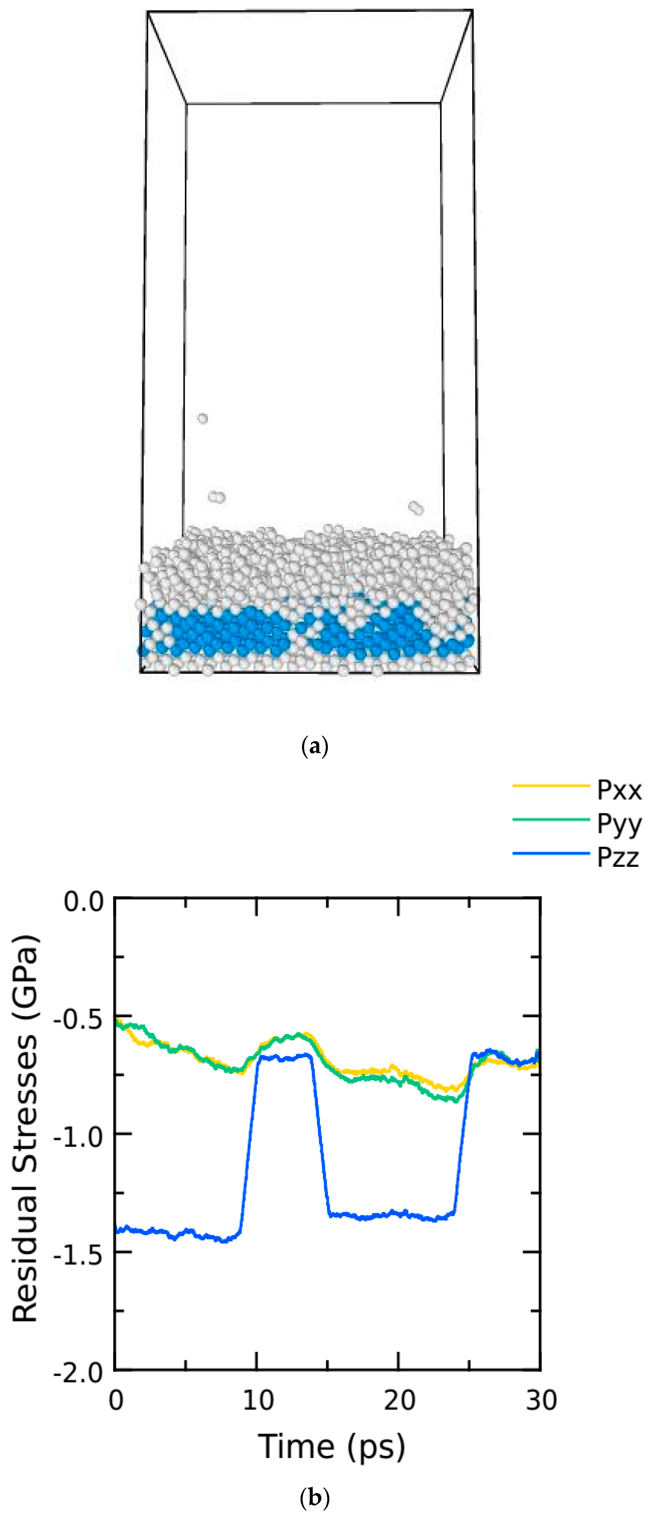
In Figure 4a, it is evident that the deposition transpired as expected. The radial distribution function peak at about 0.16 nm shows that the silica was forming at the surface level. Figure 4b shows the oxygen molecules moving towards the silicon surface and interacting with silicon to form SiO2. Blue-colored molecules are oxygen molecules, and red and yellow denote silicon atoms. four.
In Figure 5, we present stress distributions over one complete deposition cycle. The solid yellow line represents normal stress in the x-direction (Px), solid green represents normal stress in the y direction, and the solid blue line depicts normal stress in the z-direction (Pz). Stress values were computed as ensemble averages of atomic stresses in each cycle. All the stresses, Px, Py, and Pz, were compressive within the layer surface and substrate.
7. Conclusions
This study outlines a standard process for the Silica deposition process. Utilizing the ReaxFF force field, superior predictions of amorphous silica’s structure and mechanical properties were achieved compared to those obtained using other force fields. The variations in Young’s modulus and strength were attributed to strain rate, cooling rate, and temperature, with strain rate exerting the most pronounced influence, as shown in Table 3. The obtained stress–strain behavior is in good agreement with simulation-derived results published previously. However, the validation of the experimental results for amorphous silica glass was not conclusive, requiring improvements in the parameters for the reactive force field. However, the residual stresses observed during the deposition process evaluated confirmed that compressive stress forms as depth increases, also increasing stress.
This research investigated the stresses that emerge during the initial silicon dioxide film growth phase. Experimental stress analysis typically covers films with thicknesses of about 150 nm, for which simulations could not be complemented. The failure to validate the experimental results opens up potential future avenues of study.
Author Contributions
Conceptualization, Formal Analysis, Methodology, Writing—Original Draft, S.S.; STEM Data Curation, Writing—Review and Editing, LAMMPS Data Analysis, N.I.; Review and Authorization, R.M.; Funding acquisition, Project Administration, Resources, Supervision, S.A. All authors have read and agreed to the published version of the manuscript.
Funding
National Science Foundation (Grant ECCS-2025462). Department of Defense [Contract #W911QY2220006].
Institutional Review Board Statement
Not applicable.
Informed Consent Statement
Not applicable.
Data Availability Statement
The data presented in this study are available on request from the corresponding author. The data is not publicly available due to academic restrictions.
Conflicts of Interest
The authors declare no conflict of interest.
References
- Ping, S.; Jie, L.; Gao, S.; Li, P.; Wang, X.; Wu, S.; Ma, Z. PECVD grown SiO2 film process optimization. In Silicon Photonics VI; SPIE: Bellingham, WA, USA, 2011; Volume 7943, pp. 352–357. [Google Scholar]
- Mackenzie, K.D.; Johnson, D.J.; DeVre, M.W.; Westerman, R.J.; Reelfs, B.H. Stress control of Si-based PECVD dielectrics. In Proceedings of the 207th Electrochemical Society Meeting, Quebec, QC, Canada, 15–20 May 2005; pp. 148–159. [Google Scholar]
- BIOVIA Materials Studio. Available online: https://www.3ds.com/products/biovia/materials-studio (accessed on 12 October 2023).
- SiO₂ mp-6930. Available online: https://next-gen.materialsproject.org/materials/mp-6930#properties (accessed on 12 October 2023).
- Kulkarni, A.D.; Truhlar, D.G.; Goverapet Srinivasan, S.; van Duin AC, T.; Norman, P.; Schwartzentruber, T.E. Oxygen interactions with silica surfaces: Coupled cluster and density functional investigation and the development of a new ReaxFF potential. J. Phys. Chem. C 2013, 117, 258–269. [Google Scholar] [CrossRef]
- Thompson, A.P.; Aktulga, H.M.; Berger, R.; Bolintineanu, D.S.; Brown, W.M.; Crozier, P.S.; in’t Veld, P.J.; Kohlmeyer, A.; Moore, S.G.; Nguyen, T.D.; et al. LAMMPS—A flexible simulation tool for particle-based matrials modeling at the atomic, meso, and continuum scales. Comput. Phys. Commun. 2022, 271, 10817. [Google Scholar] [CrossRef]
- Available online: https://en.wikipedia.org/wiki/Silicon_dioxide (accessed on 12 October 2023).
- Grigoriev, F.V.; Sulimov, A.V.; Katkova, E.V.; Kochikov, I.V.; Kondakova, O.A.; Sulimov, V.B.; Tikhonravov, A.V. Computational Experiments on Atomistic Modeling of Thin Film Deposition. Appl. Opt. 2017, 56, C87–C90. [Google Scholar] [CrossRef] [PubMed]
- Grigoriev, F.V.; Sulimov, V.B. Atomistic Simulation of Physical Vapor Deposition of Optical Thin Films. Nanomaterials 2023, 13, 1717. [Google Scholar] [CrossRef] [PubMed]
Figure 1.
Schematic of PECVD.
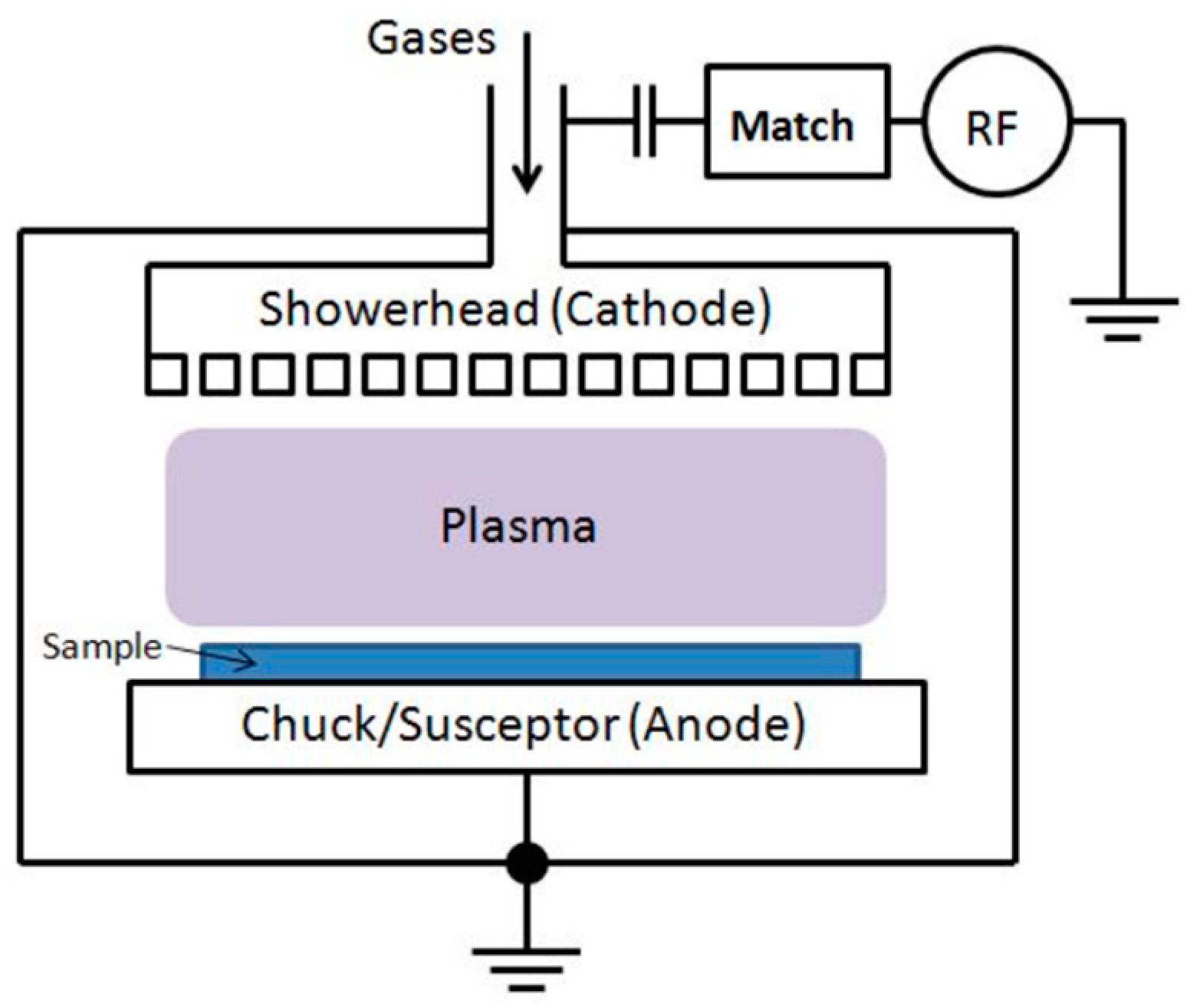
Figure 2.
Silica crystal structure modeled in Material Studio.
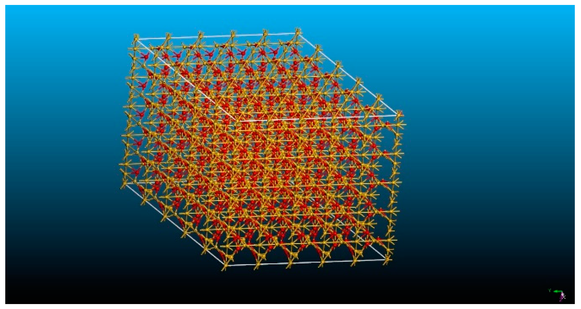
Figure 3.
Extrinsic stress characteristics according to LAMMPS (a,b).

Figure 4.
(a) Radial distribution function of Layer 1. (b) Random O2 molecules being deposited on Si substrate.
Figure 4.
(a) Radial distribution function of Layer 1. (b) Random O2 molecules being deposited on Si substrate.

Figure 5.
(a) Deposition process visualization using OVITO. (b) Residual stresses generated over one cycle of deposition.
Figure 5.
(a) Deposition process visualization using OVITO. (b) Residual stresses generated over one cycle of deposition.

Table 1.
PECVD Recipe for SiO2 deposition.
| Recipe Parameters |  | |
| Time | 02:00.0 | |
| Pressure | 1500 | |
| SiH4 1K | 500 | |
| SiH4 5K | -- | |
| NH3 50 | -- | |
| SF6 1K | -- | |
| AR 5K | 2000 | |
| N2O 5K | 2000 | |
| N2 5K | -- | |
| RF1 | 200 | |
| RF2 | -- |
Table 2.
SiO2 thin film parameter and response characteristics.
| SiH4 | N2O | RF Power | Thickness | Density | RF Index | Stress |
|---|---|---|---|---|---|---|
| 150 | 770 | 300 | 1488 | 2.1878 | 1.4532 | −218.752 |
| 165 | 840 | 330 | 1806 | 2.1892 | 1.4583 | −279.463 |
| 135 | 700 | 270 | 1457 | 2.1973 | 1.4563 | −319.317 |
Table 3.
Output response from LAMMPS.
| Sr No. | Temperature (K) | Strain Rate (s−1) | Young’s Modulus (GPA) |
|---|---|---|---|
| 1 | 300 | 105 | 61.38 |
| 2 | 300 | 107 | 65.55 |
| 3 | 300 | 109 | 75.49 |
| 4 | 300 | 1011 | 78.21 |
Disclaimer/Publisher’s Note: The statements, opinions and data contained in all publications are solely those of the individual author(s) and contributor(s) and not of MDPI and/or the editor(s). MDPI and/or the editor(s) disclaim responsibility for any injury to people or property resulting from any ideas, methods, instructions or products referred to in the content. |
© 2023 by the authors. Licensee MDPI, Basel, Switzerland. This article is an open access article distributed under the terms and conditions of the Creative Commons Attribution (CC BY) license (https://creativecommons.org/licenses/by/4.0/).
Share and Cite
MDPI and ACS Style
Shendokar, S.; Ingle, N.; Mohan, R.; Aravamudhan, S. Evaluating Stresses in SiO2 Thin Films Using Molecular Dynamics Simulations. Eng. Proc. 2023, 56, 230. https://doi.org/10.3390/ASEC2023-16369
AMA Style
Shendokar S, Ingle N, Mohan R, Aravamudhan S. Evaluating Stresses in SiO2 Thin Films Using Molecular Dynamics Simulations. Engineering Proceedings. 2023; 56(1):230. https://doi.org/10.3390/ASEC2023-16369
Chicago/Turabian StyleShendokar, Sachin, Nikhil Ingle, Ram Mohan, and Shyam Aravamudhan. 2023. "Evaluating Stresses in SiO2 Thin Films Using Molecular Dynamics Simulations" Engineering Proceedings 56, no. 1: 230. https://doi.org/10.3390/ASEC2023-16369