

Energy Conversion Optimization Method in Nano-Grids Using Variable Supply Voltage Adjustment Strategy Based on a Novel Inverse Maximum Power Point Tracking Technique (iMPPT)

 ,
,  , ,
, ,
Abstract
:1. Introduction
- 0
- Variable voltage nano-grid architecture
- 1
- Variable DC bus voltage
- 2
- Photovoltaic panels (PV) array
- 3
- Boost converter for the PV array
- 4
- Micro wind turbine
- 5
- Micro wind turbine boost converter
- 6
- Battery bank
- 7
- Battery bank bi-directional converter
- 8
- AC public grid
- 9
- AC public grid bi-directional power stage
- 10
- AC-DC PWM controlled inverter/rectifier
- 11
- DC-DC bi-directional converter
- 12
- DC-Bus voltage reference
- 13
- AC loads
- 14
- AC loads buck/step-down converters
- 15
- DC loads
- 16
- DC loads buck/step-down converters
- 17
- Logic control unit/specialized embedded computing system
- 17a
- Power measurement module
- 17b
- Power value logic decisional module
- 17c
- Inverse maximum power point tracking (iMPPT) algorithm that minimizes “PB”
- 17d
- Inverse maximum power point tracking (iMPPT) algorithm that maximizes “PB”
- 18
- Centralized loads measurement module
- 19
- Centralized unidirectional power sources measurement module
- 20
- Centralized bidirectional power sources measurement module
- 21
- PV array power measurement module
- 22
- Wind turbine power measurement module
- 23
- Battery bank power measurements module
- 24
- AC public grid power measurement module
- 25
- DC loads power measurement module
- 26
- AC loads power measurement module
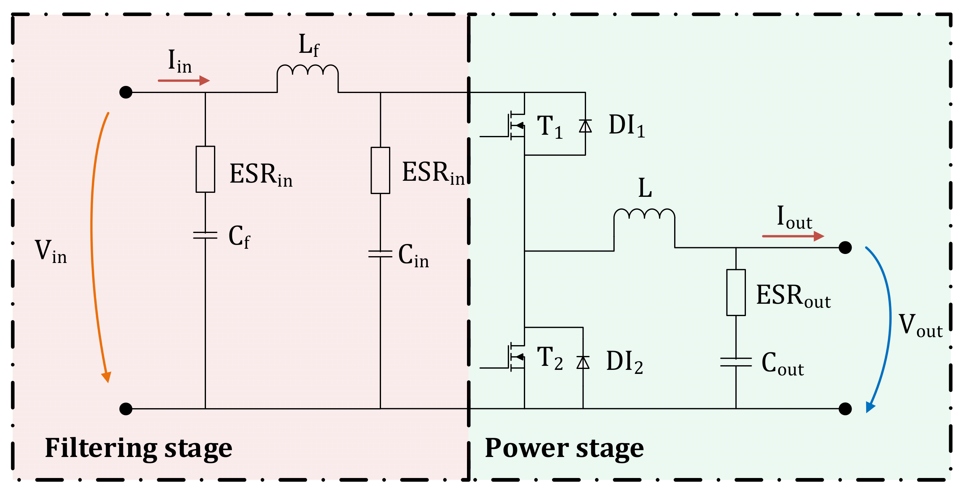
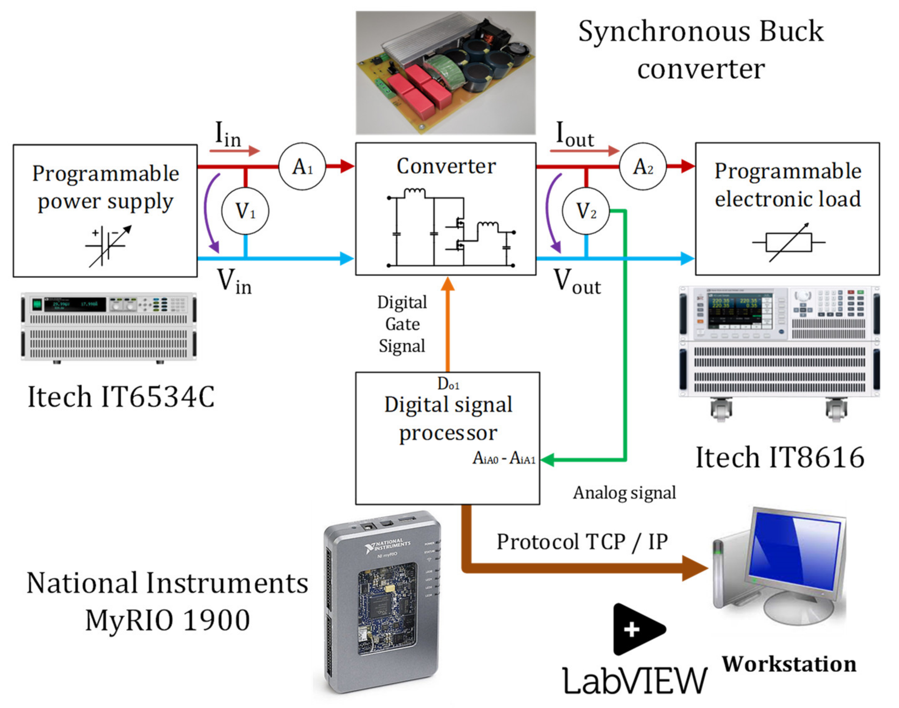
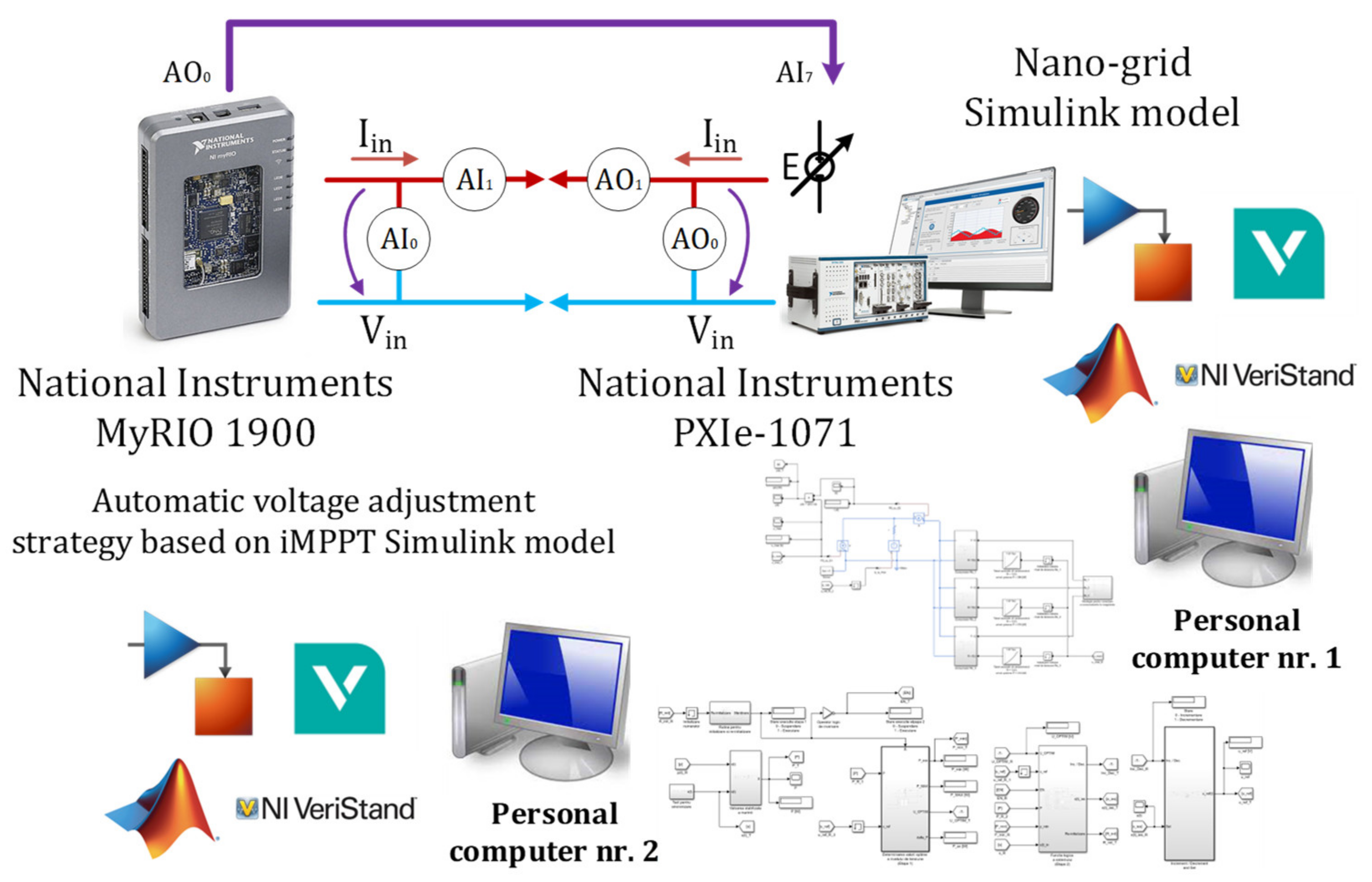
2. Methodology and Experimental Setup for Proving the Main Concept
- -
- programmable DC voltage power supply Itech IT6534C (light blue mark)
- -
- AXIO MET AX-582B multimeter for measuring input current (blue mark)
- -
- AXIO MET AX-582B multimeter for measuring input voltage (pink mark)
- -
- power resistor with a value of 1 Ω for simulating the cable length (gray mark)
- -
- National Instruments MyRIO 1900—embedded development kit (orange mark)
- -
- synchronous buck step-down converter (dark yellow mark)
- -
- AXIO MET AX-582B multimeter for measuring output current (dark blue mark)
- -
- AXIO MET AX-582B multimeter for measuring output voltage (dark brown mark)
- -
- adjustable sources for powering annex modules (light green mark)
- -
- IT8616 programmable electronic load (light yellow mark)
- -
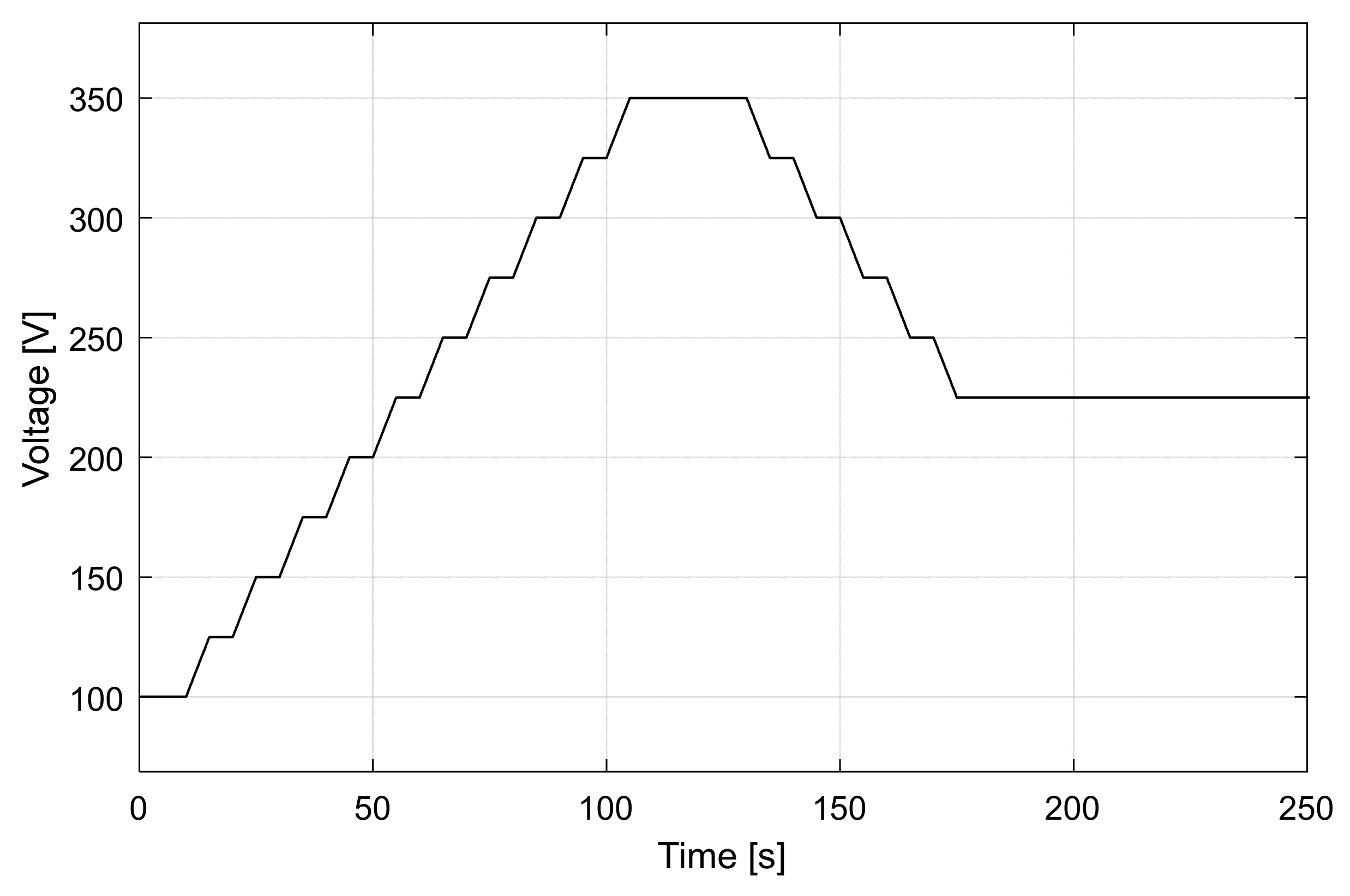
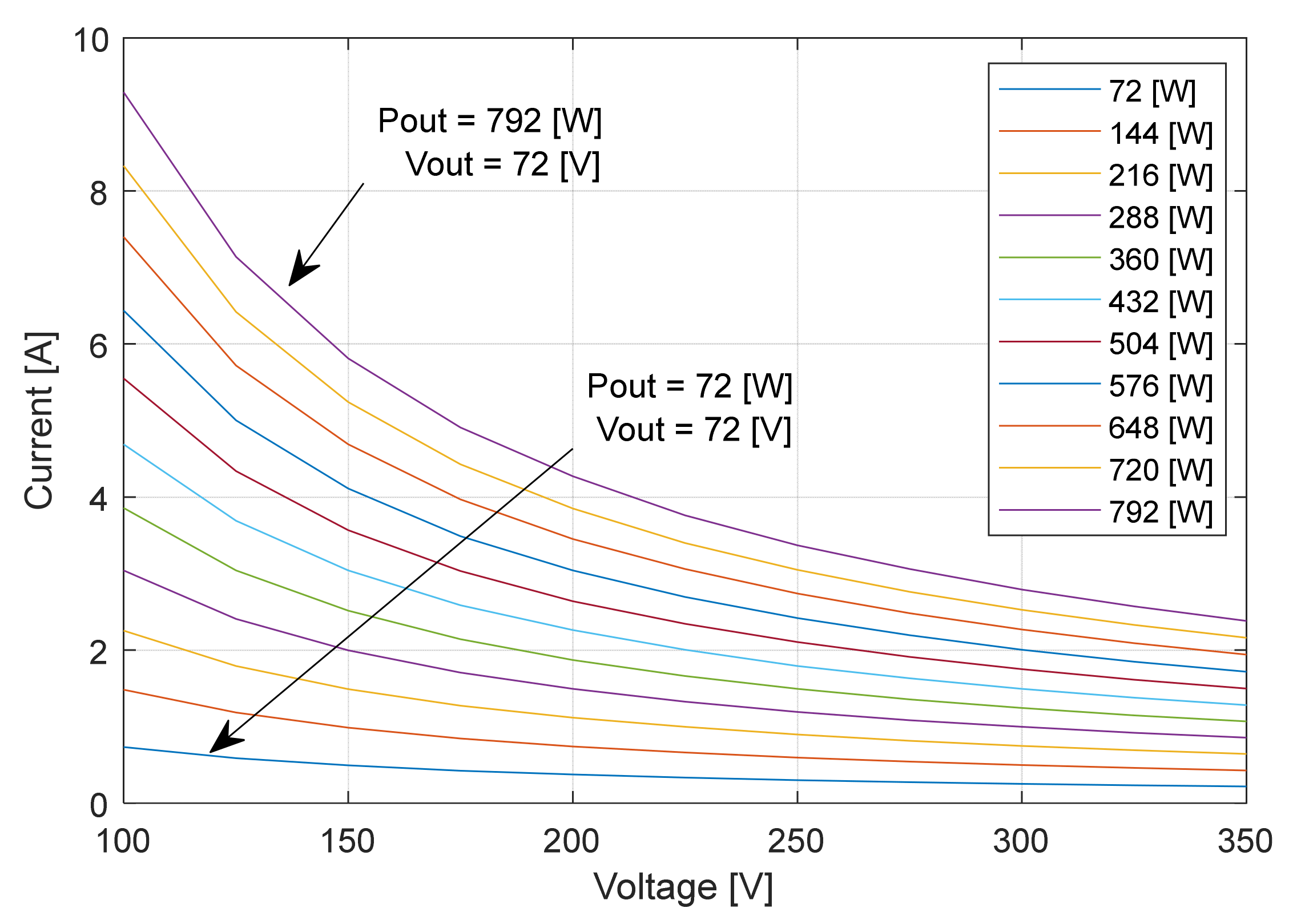
- At the input of the converter, the initial input voltage value will be set at 100 V and data-points will be collected in a summary table; after this step the input voltage value will be increased by another 25 V and data-points will be collected again in the summary table until the final value of 350 V is reached.
- -
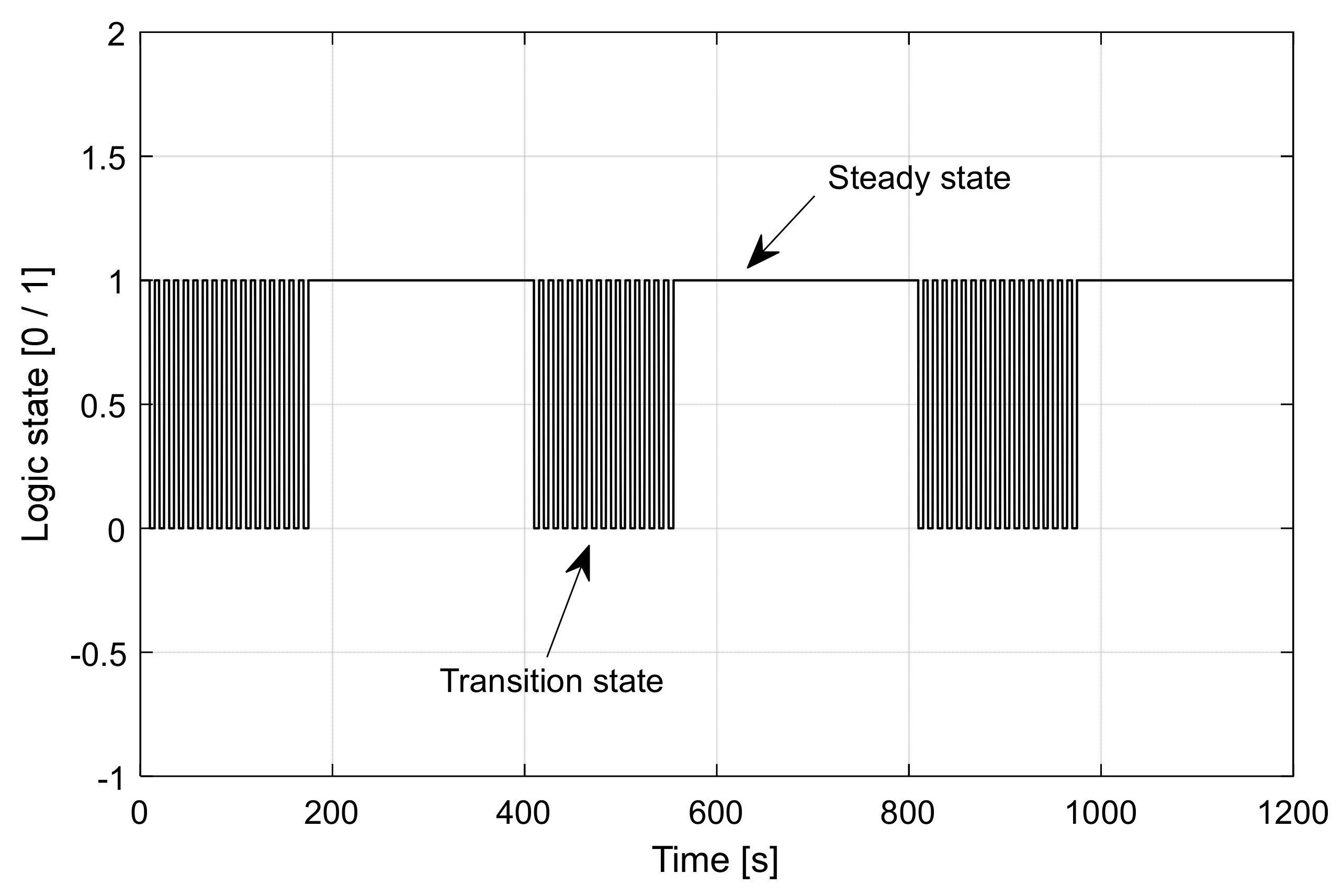
- The output voltage will be kept constant at 72 V using the NI MyRIO embedded controller, with the control law implemented. The control loop runs at a 10 ms time step within LabVIEW and MyRIO.
- -
- The PID controller coefficients were set empirically based on the concept of minimizing the closed loop system’s error in the shortest possible time interval (a Ziegler-Nichols PID tuning method approach based on Equations (3), (4) and (6)). The determined controller coefficients are kP = 0.001 and kI = 0.008, kD = 0 and the saturation or limit range for the PWM signal and the duty cycle is [0, 0.95]. The controller is a classical PID model implemented in LabVIEW based on the classical mathematical approach of a simple (non-parallel) PID controller [18,19].
- -
- Using the programmable electronic load, constant power values will be set at the output of the power electronics converter.
- -
- At each new value of the output power, a complete input voltage sweep cycle will be performed, and the data-point will be recorded in a summary table.
- -
- Using the input and output values of voltage and current, the input and output power, the conversion efficiency, the overall converter losses and the input impedance values will be determined.
- -
- Based on all data-points and the determined parameters, functional characteristic curves of the power electronics converter will be plotted and analyzed in different situations.
- -
- Two PCs running NI 2021 SP1 Software Bundle including VeriStand (same version).
- -
- MyRIO-1900 embedded controller.
- -
- NI PXIe-1071 Hardware In the Loop Real-Time simulation computer.
- -
- MathWorks Matlab-Simulink R2018b + NI VeriStand model framework.
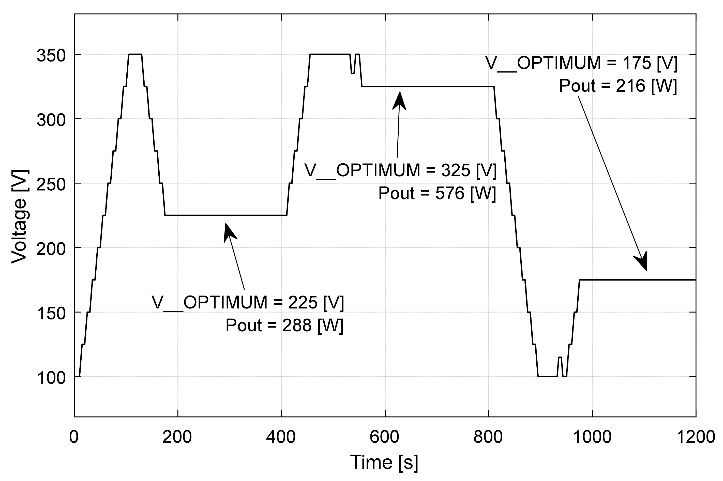
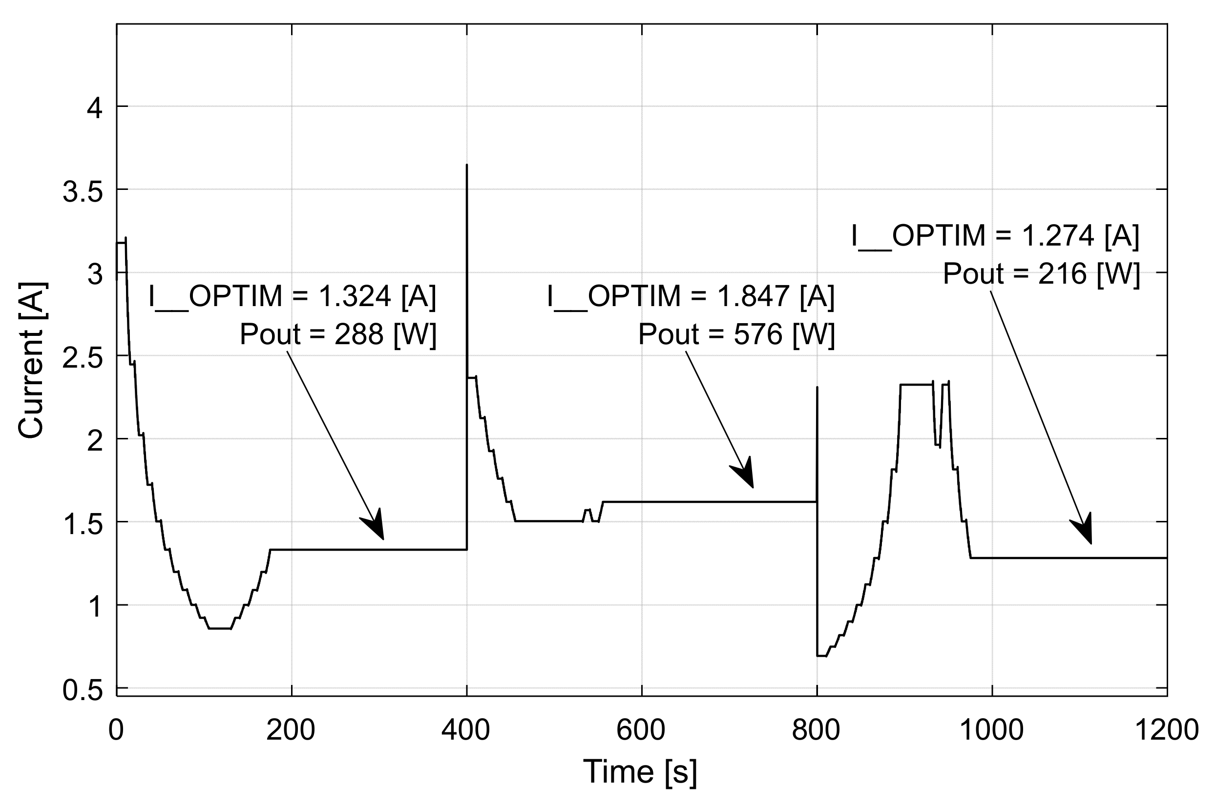
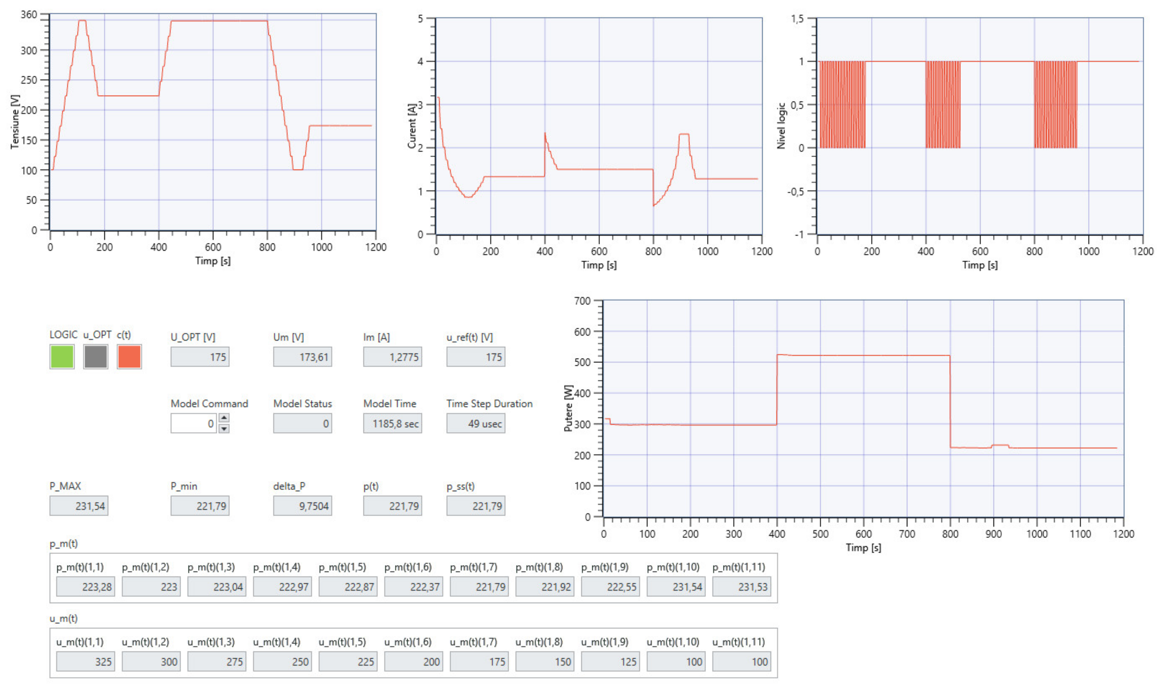
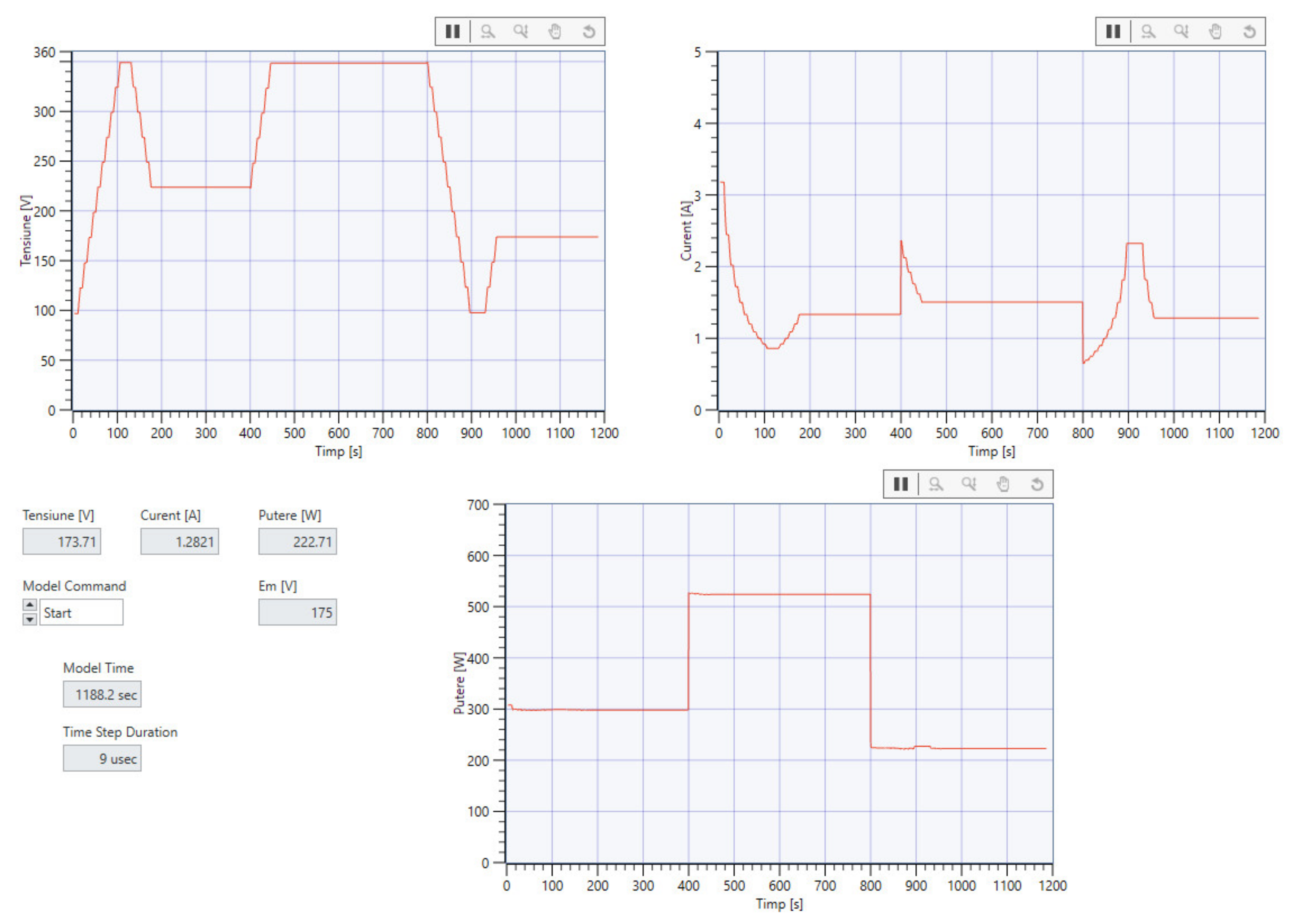
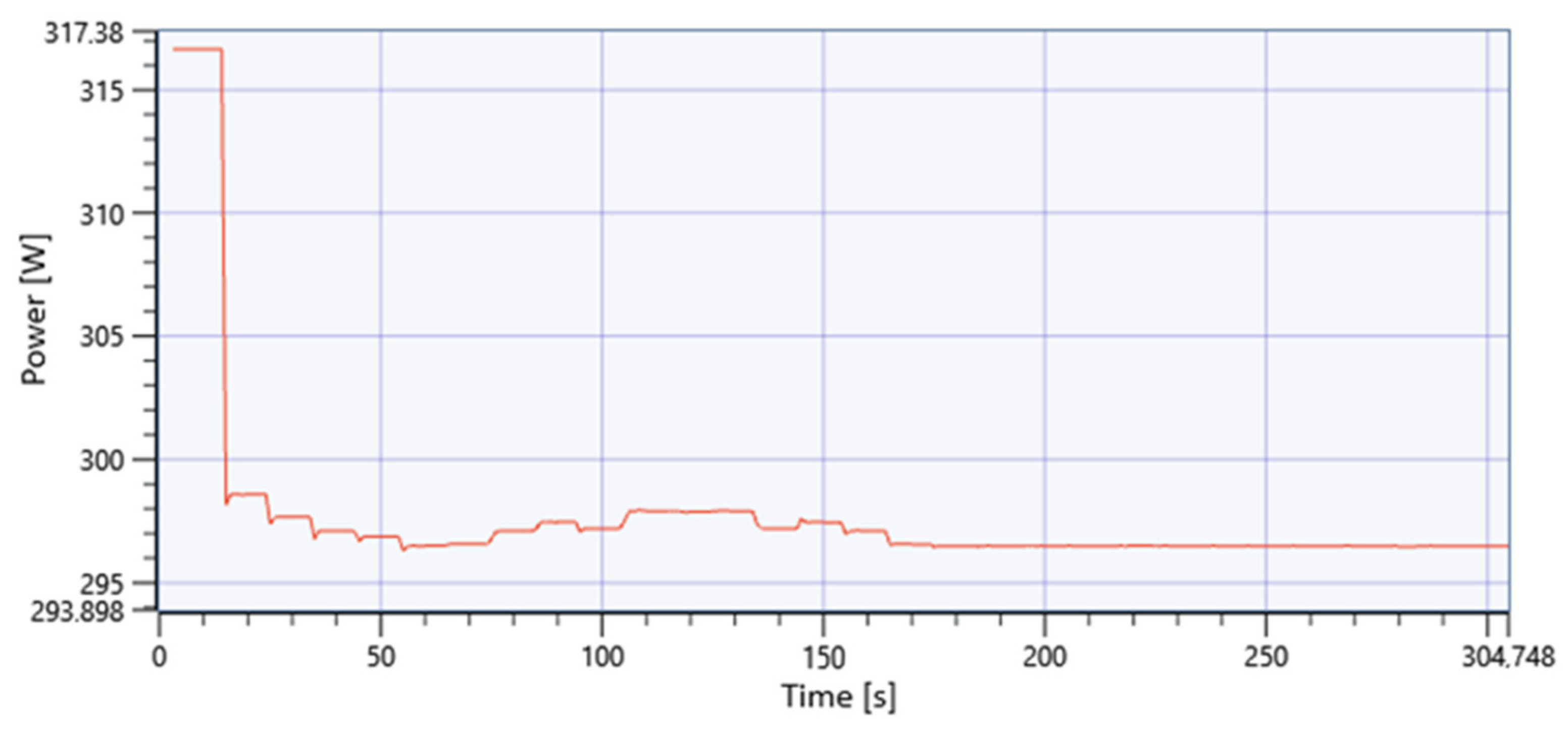
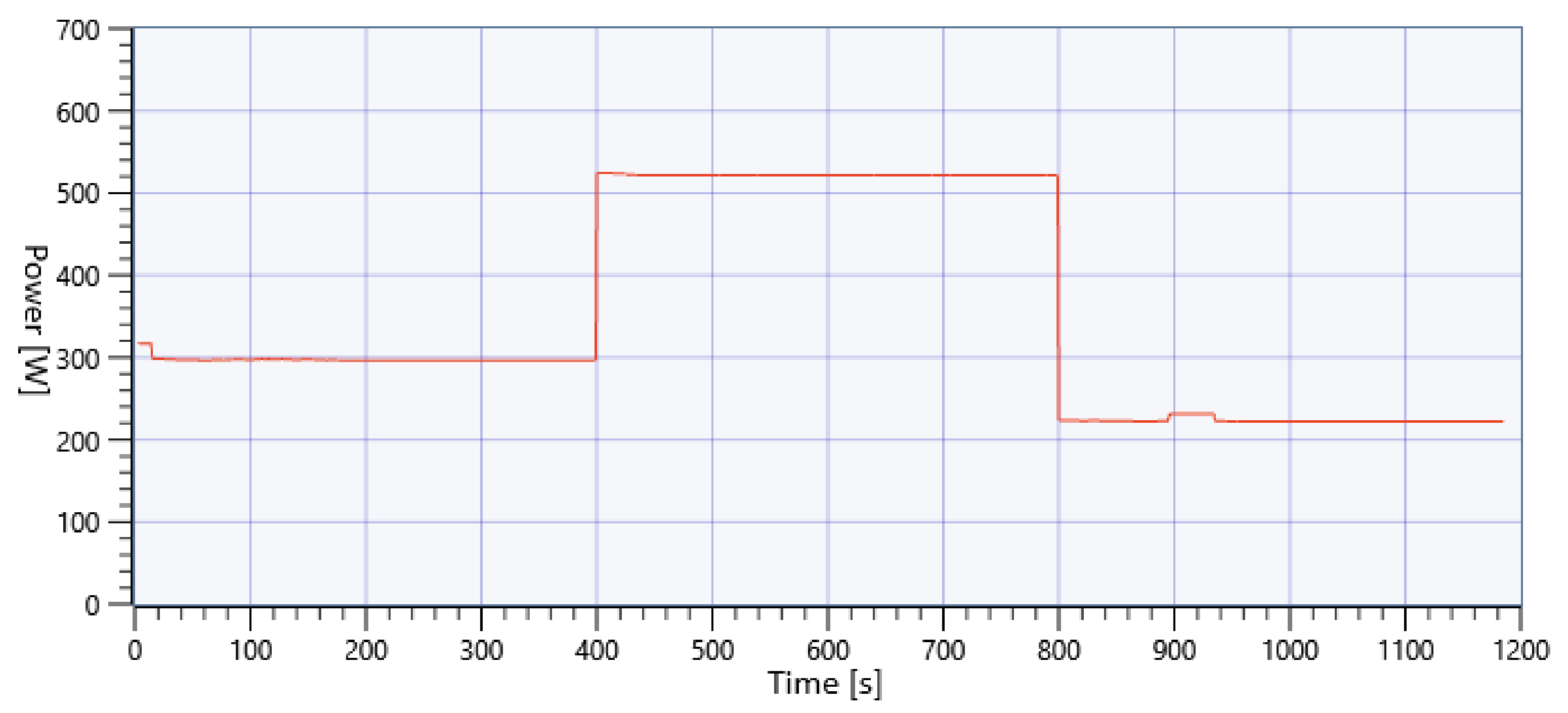
3. Results
4. Discussion
5. Conclusions
- -
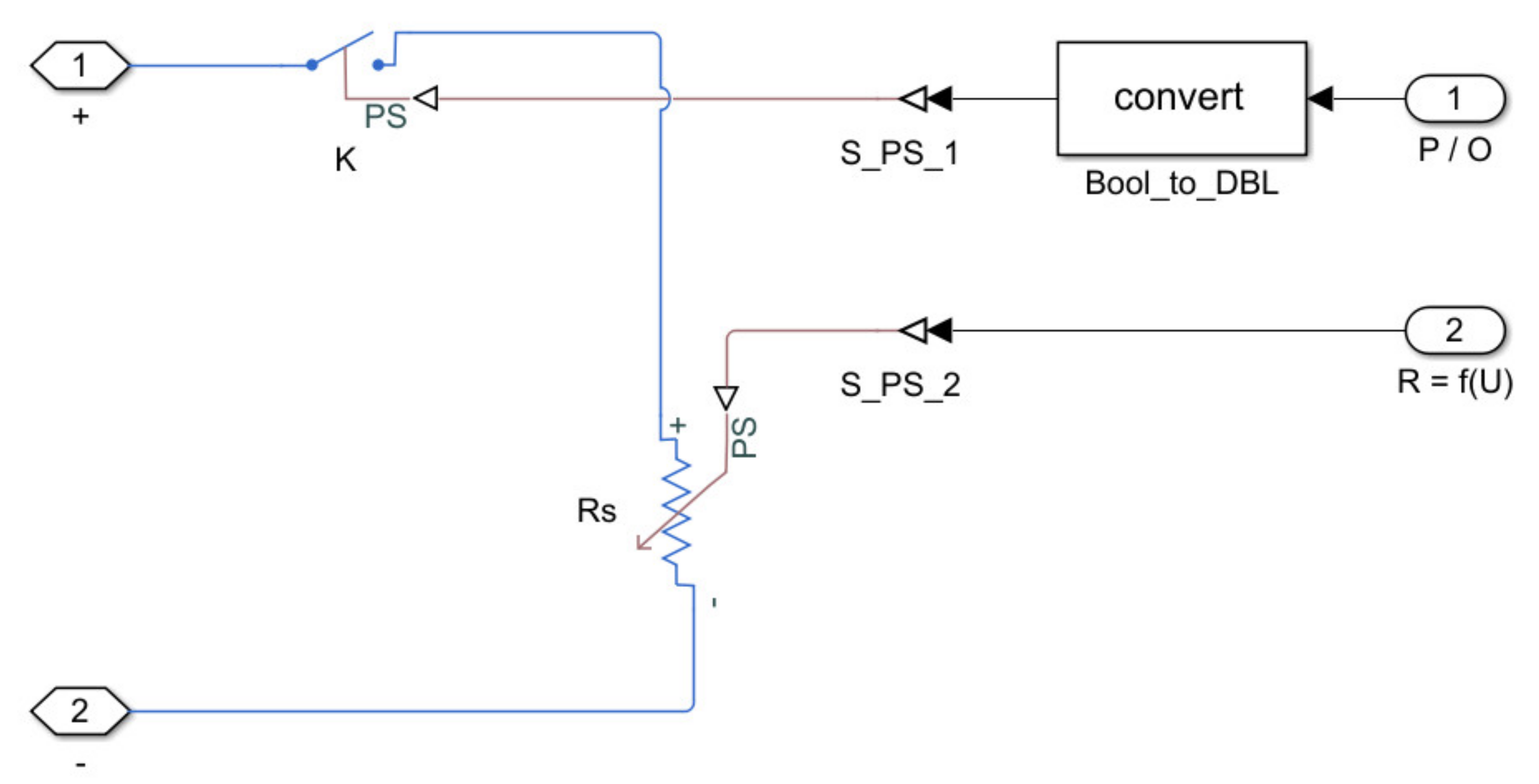
- Based on representative functional characteristics of consumers (e.g., characteristic curve I = f(V)), it is possible to identify the operating mode [34].
- -
- In the case of a regulated voltage source, the equivalent circuit can be reduced to a constant power consumer load from the point of view of the input side [34].
- -
- The converter adjusts the impedance to serve the final consumer load at the optimal parameters [34].
- -
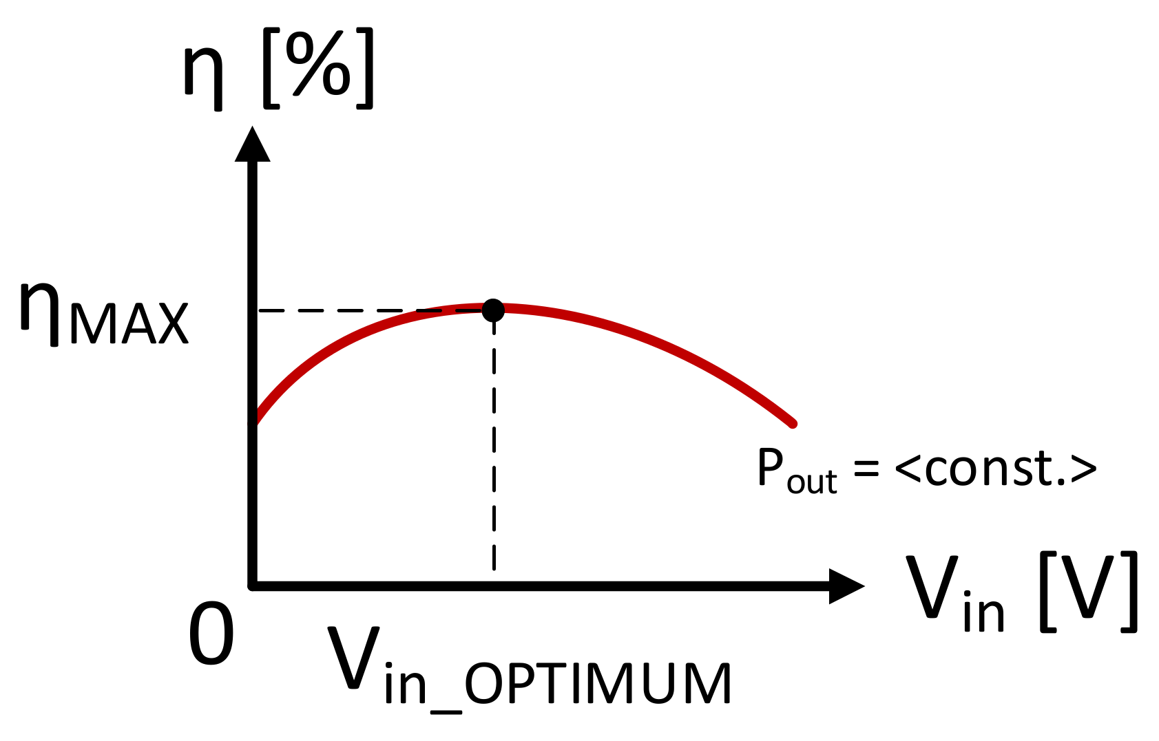
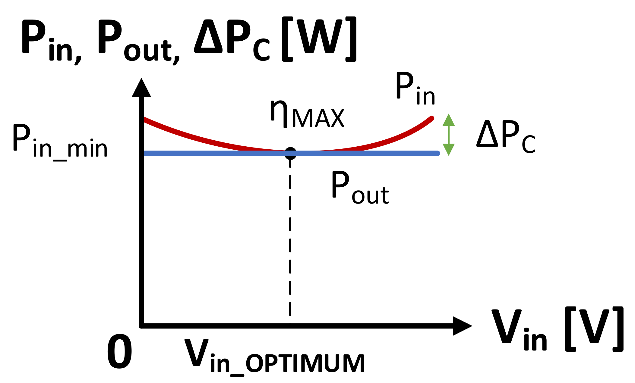
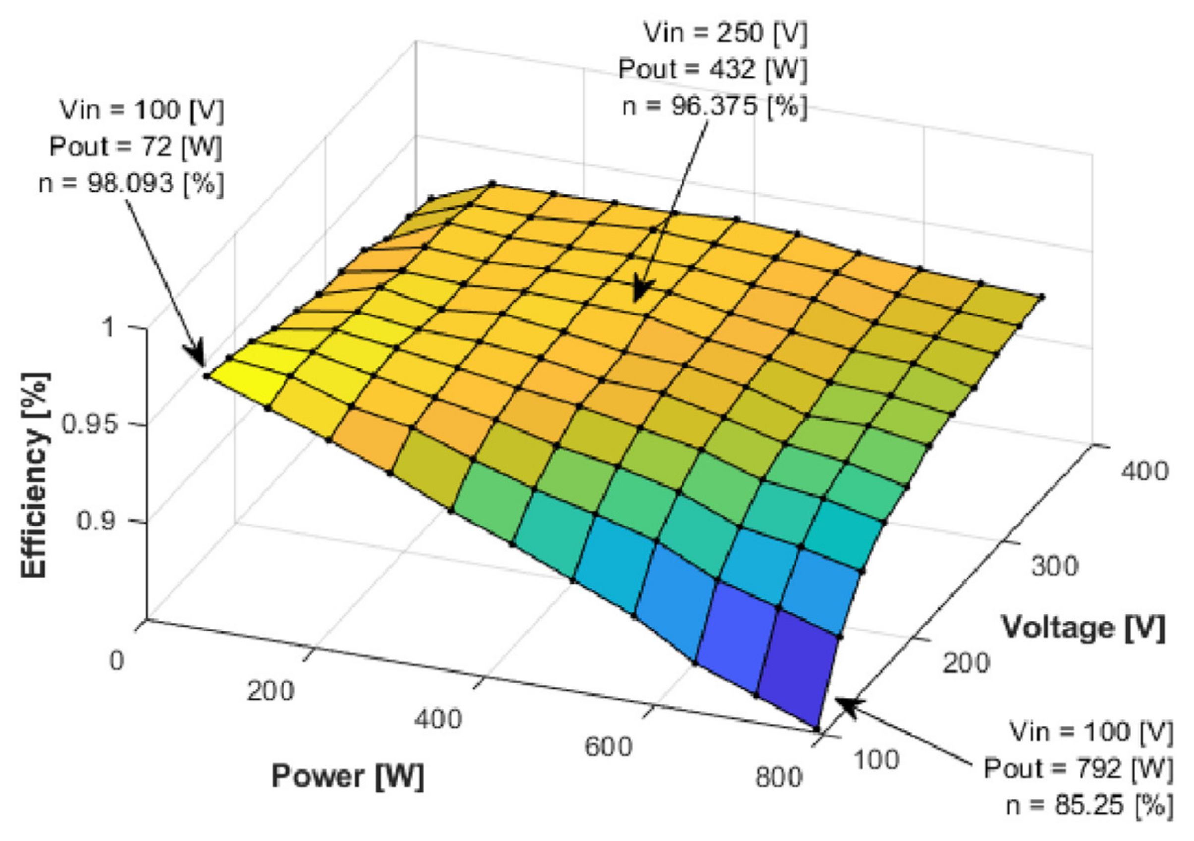
- The input voltage level can be adjusted in such a way that the conversion efficiency of a regulated switched mode power supply can be improved.
- -
- The novel proposed iMPPT method can improve the energy conversion ratio from 85% up to approximately 10% in case of an output power level of 800 W served by a synchronous buck converter at the input voltage level of 350 V. The total amount of recovered power in this situation can be approximately 100 W.
6. Patents
Author Contributions
Funding
Data Availability Statement
Conflicts of Interest
References
- Rodriguez-Otero, M.A.; O’Neill-Carrillo, E. Efficient Home Appliances for a Future DC Residence. In Proceedings of the 2008 IEEE Energy 2030 Conference, Atlanta, GA, USA, 17–18 November 2008; pp. 1–6. [Google Scholar] [CrossRef]
- Cordova-Fajardo, M.A.; Tututi, E.S. Incorporating home appliances into a DC home nanogrid. J. Phys. Conf. Ser. 2019, 1221, 012048. [Google Scholar] [CrossRef]
- Chub, A.; Vinnikov, D.; Kosenko, R.; Liivik, E.; Galkin, I. Bidirectional DC–DC Converter for Modular Residential Battery Energy Storage Systems. IEEE Trans. Ind. Electron. 2020, 67, 1944–1955. [Google Scholar] [CrossRef]
- Sabry, A.H.; Shallal, A.H.; Hameed, H.S.; Ker, P.J. Compatibility of household appliances with DC microgrid for PV systems. Heliyon 2020, 6, e05699. [Google Scholar] [CrossRef] [PubMed]
- Elvira, D.G.; Blaví, H.V.; Pastor, À.C.; Salamero, L.M. Efficiency Optimization of a Variable Bus Voltage DC Microgrid. Energies 2018, 11, 3090. [Google Scholar] [CrossRef]
- Dong, D.; Cvetkovic, I.; Boroyevich, D.; Zhang, W.; Wang, R. Mattavelli. Grid-Interface Bidirectional Converter for Residential DC Distribution Systems—Part One: High-Density Two-Stage Topology. IEEE Trans. Power Electron. 2013, 28, 1655–1666. [Google Scholar] [CrossRef]
- Teodosescu, P.D.; Pintilie, L.N.; Iuora, A.M.; Salcu, S.I.; Bojan, M. Micro-Grid Has Bidirectional Sources which Inject or Absorb Energy from Micro-Grid Based on Power converters with Two Conversion Stages, in which Alternating Current Consumers and Direct Current Consumers Absorb Energy. Available online: https://www.webofscience.com/wos/diidw/full-record/DIIDW:202073761E (accessed on 7 September 2023).
- Nicolae, P.L. Research Aimed at Electricity Management in Electronic Systems with Renewable Sources. Ph.D. Thesis, Technical University of Cluj-Napoca, Cluj-Napoca, Romania, 2023. under press.
- Moussa, S.; Ghorbal, M.J.-B.; Slama-Belkhodja, I. Bus voltage level choice for standalone residential DC nano grid. Sustain. Cities Soc. 2019, 46, 101431. [Google Scholar] [CrossRef]
- Li, T.; Ji, Z.C. Intelligent inverse control to maximum power point tracking control strategy of wind energy conversion system. In Proceedings of the 2011 Chinese Control and Decision Conference (CCDC), Mianyang, China, 23–25 May 2011; IEEE: Piscataway Township, NJ, USA, 2011; pp. 970–974. [Google Scholar] [CrossRef]
- Teodosescu, P.D.; Pintilie, L.N.; Iuoras, A.M.; Salcu, S.I.; Bojan, M. Micro-Grid of Variable DC Voltage and Its Control Method—Official Bulletin of Industrial Property. RO134348A0. Available online: https://osim.ro/wp-content/uploads/Publicatii-OSIM/BOPI-Inventii/2020/bopi_inv_07_2020.pdf (accessed on 7 September 2023).
- Anand, S.; Fernandes, B.G. Optimal voltage level for DC microgrids. In Proceedings of the IECON 2010—36th Annual Conference on IEEE Industrial Electronics Society, Glendale, AZ, USA, 7–10 November 2010; pp. 3034–3039. [Google Scholar] [CrossRef]
- Mallik, A.; Khaligh, A. Maximum Efficiency Tracking of an Integrated Two-Staged AC–DC Converter Using Variable DC-Link Voltage. IEEE Trans. Ind. Electron. 2018, 65, 8408–8421. [Google Scholar] [CrossRef]
- Liu, Q.; Wu, X.; Zhao, M.; Wang, L.; Shen, X. 30–300 mV input, ultra-low power, self-startup DC-DC boost converter for energy harvesting system. In Proceedings of the 2012 IEEE Asia Pacific Conference on Circuits and Systems, Kaohsiung, Taiwan, 2–5 December 2012; pp. 432–435. [Google Scholar] [CrossRef]
- Suciu, V.M.; Salcu, S.I.; Pintilie, L.N.; Teodosescu, P.D.; Mathe, Z. Theoretical efficiency analysis of a buck-boost converter for wide voltage range operation. In Proceedings of the 2018 10th International Conference on Electronics, Computers and Artificial Intelligence (ECAI), Iasi, Romania, 28–30 June 2018; pp. 1–4. [Google Scholar] [CrossRef]
- Mulligan, M.D.; Broach, B.; Lee, T.H. A constant-frequency method for improving light-load efficiency in synchronous buck converters. IEEE Power Electron. Lett. 2005, 3, 24–29. [Google Scholar] [CrossRef]
- Zhou, X.; Donati, M.; Amoroso, L. Improved light-load efficiency for synchronous rectifier voltage regulator module. IEEE Trans. Power Electron. 2000, 15, 826–834. [Google Scholar] [CrossRef]
- PID ‘Proportional, Integral, and Derivative’ Control Theory. Crystal Instruments, 24 August 2020. Available online: https://www.crystalinstruments.com/blog/2020/8/23/pid-control-theory (accessed on 10 July 2023).
- Borase, R.P.; Maghade, D.K.; Sondkar, S.Y.; Pawar, S.N. A review of PID control, tuning methods and applications. Int. J. Dyn. Control. 2021, 9, 818–827. [Google Scholar] [CrossRef]
- Omar, O.A.; Marei, M.I.; Attia, M.A. Comparative Study of AVR Control Systems Considering a Novel Optimized PID-Based Model Reference Fractional Adaptive Controller. Energies 2023, 16, 830. [Google Scholar] [CrossRef]
- Alghamdi, S.; Sindi, H.F.; Rawa, M.; Alhussainy, A.A.; Calasan, M.; Micev, M.; Ali, Z.M.; Abdel Aleem, S.H. Optimal PID Controllers for AVR Systems Using Hybrid Simulated Annealing and Gorilla Troops Optimization. Fractal Fract. 2023, 6, 682. [Google Scholar] [CrossRef]
- Ozgenc, B.; Ayas, M.S.; Altas, I.H. Performance improvement of an AVR system by symbiotic organism search algorithm-based PID-F controller. Neural Comput. Appl. 2022, 34, 7899–7908. [Google Scholar] [CrossRef]
- Mohd Tumari, M.Z.; Ahmad, M.A.; Suid, M.H.; Hao, M.R. An Improved Marine Predators Algorithm-Tuned Fractional-Order PID Controller for Automatic Voltage Regulator System. Fractal Fract. 2023, 7, 561. [Google Scholar] [CrossRef]
- Erickson, R.W. Maksimović, Fundamentals of Power Electronics; Springer International Publishing: Cham, Switzerland, 2020. [Google Scholar] [CrossRef]
- Simion, E. Electrotehnică—Manual Pentru Subingineri. In Manuale Pentru Electrotehnică Generală; no. 12000 Ex SP.; Editura Didactică și Pedagogică: Bucuresti, Romania, 1977; Volume 1. [Google Scholar]
- Useful Applications for Electronic Loads (2) Non-Linear Modes—KIKUSUI AMERICA, INC. Available online: https://kikusui.co.jp/ (accessed on 24 June 2023).
- Figueiredo, R.E.; Monteiro, V.; Afonso, J.A.; Pinto, J.G.; Salgado, J.A.; Cardoso, L.A.L.; Nogueira, M.; Abreu, A.; Afonso, J.L. Efficiency Comparison of Different DC-DC Converter Architectures for a Power Supply of a LiDAR System. In Proceedings of the Sustainable Energy for Smart Cities: Second EAI International Conference, SESC 2020, Viana do Castelo, Portugal, 4 December 2020; Springer International Publishing: Cham, Switzerland, 2021; pp. 97–110. [Google Scholar] [CrossRef]
- Guy, P. Efficiency Calculations for Power Converters. Industrial and Medical Power Supplies. TDK—Lambda Americas, 5 September 2012. Available online: https://www.us.lambda.tdk.com (accessed on 7 September 2023).
- Wang, B.; Hu, Q.; Wang, Z. A High-Efficiency Double DC–DC Conversion System for a Fuel Cell/Battery Hybrid Power Propulsion System in Long Cruising Range Underwater Vehicles. Energy Fuels 2020, 34, 8872–8883. [Google Scholar] [CrossRef]
- Taufik, D. Practical Design of Buck Converter. In Proceedings of the 2008 2nd IEEE International Conference on Power and Energy PECon 2008, Johor Bahru, Malaysia, 1–3 December 2008. [Google Scholar]
- Chen, D.; Xu, L.; Yao, L. DC Voltage Variation Based Autonomous Control of DC Microgrids. IEEE Trans. Power Deliv. 2013, 28, 637–648. [Google Scholar] [CrossRef]
- Zhang, X. Impedance Control and Stability of DC/DC Converter Systems. Ph.D. Thesis, Department of Automatic Control and Systems Engineering, Faculty of Engineering, University of Sheffield, Sheffield, UK, 2016. [Google Scholar]
- Ginell, T. Why a Perfectly Stable Switch-Mode Power Supply May Still Oscillate Due to Negative Resistance. Analog Dialogue. Analog Devices. Published on March 2023. Available online: https://www.analog.com/en/analog-dialogue/raqs/raq-issue-211.html (accessed on 7 September 2023).
- MathWorks Inc. Behavioral Model of Power Converter. Average models of DC-DC Converters, SimScape Fundamentals, Published in 2022 Updated in 2023. Available online: https://www.mathworks.com/help/sps/ref/dcdcconverter.html (accessed on 7 September 2023).


| Vin [V] | Iin [A] | Pin [W] | Vout [V] | Iout [A] | Pout [W] | η [%] | ΔPC [W] | Zin [Ω] |
|---|---|---|---|---|---|---|---|---|
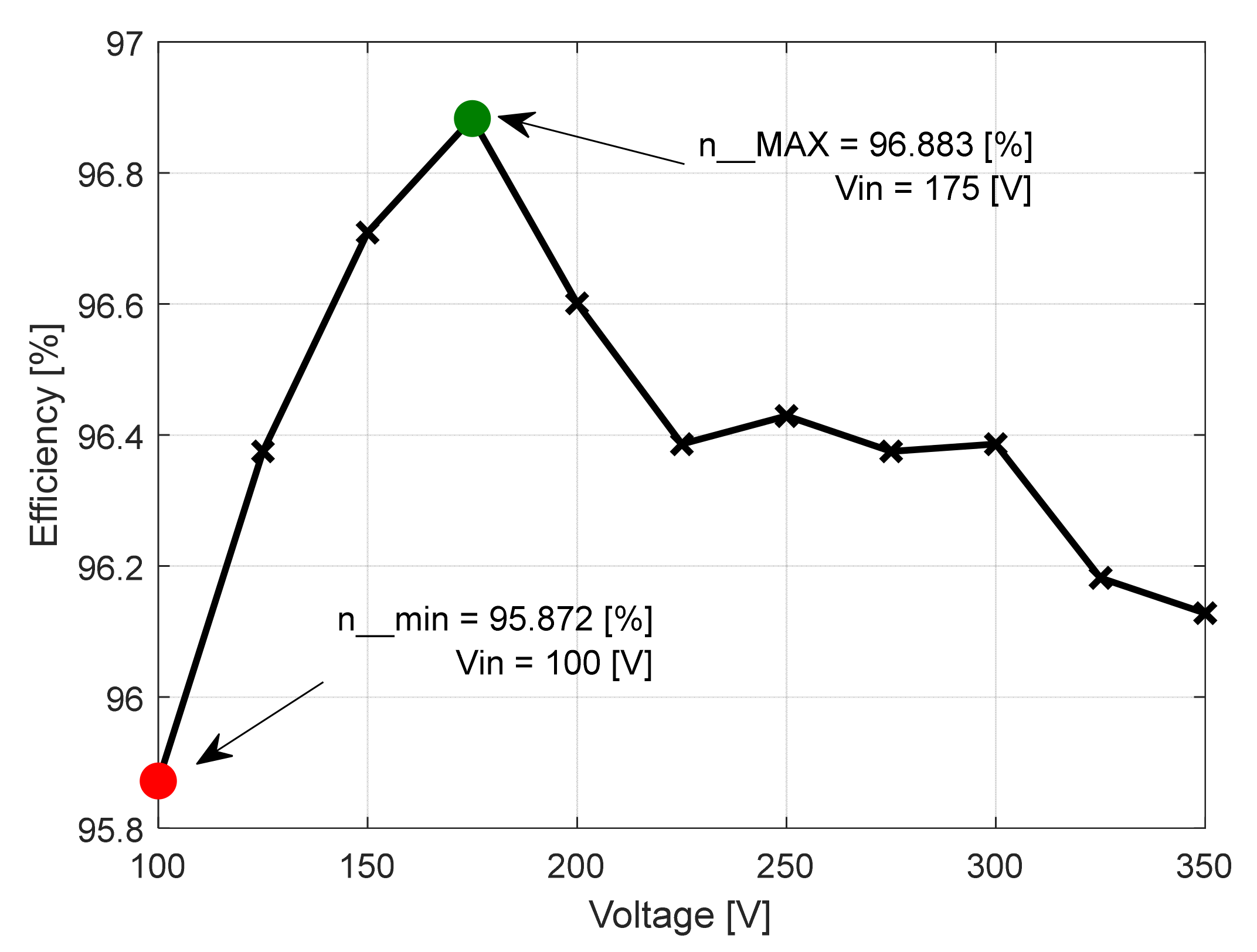
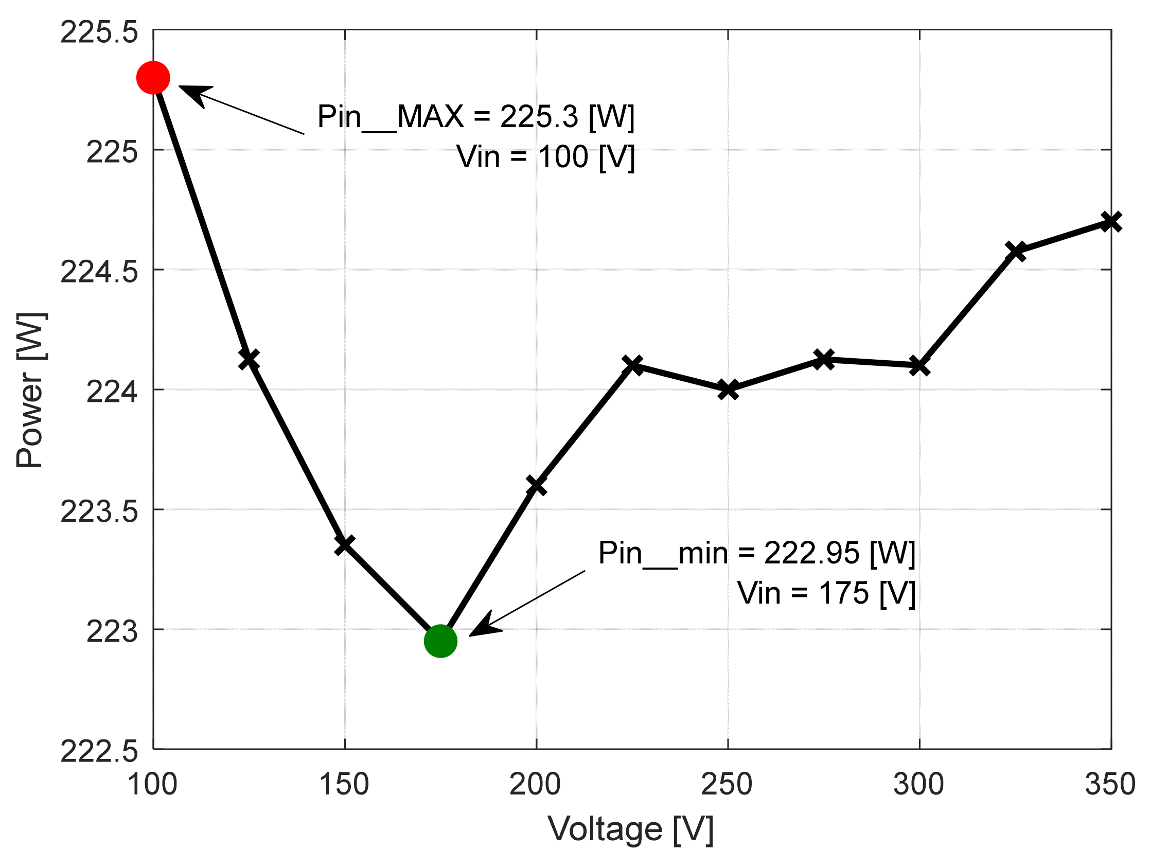
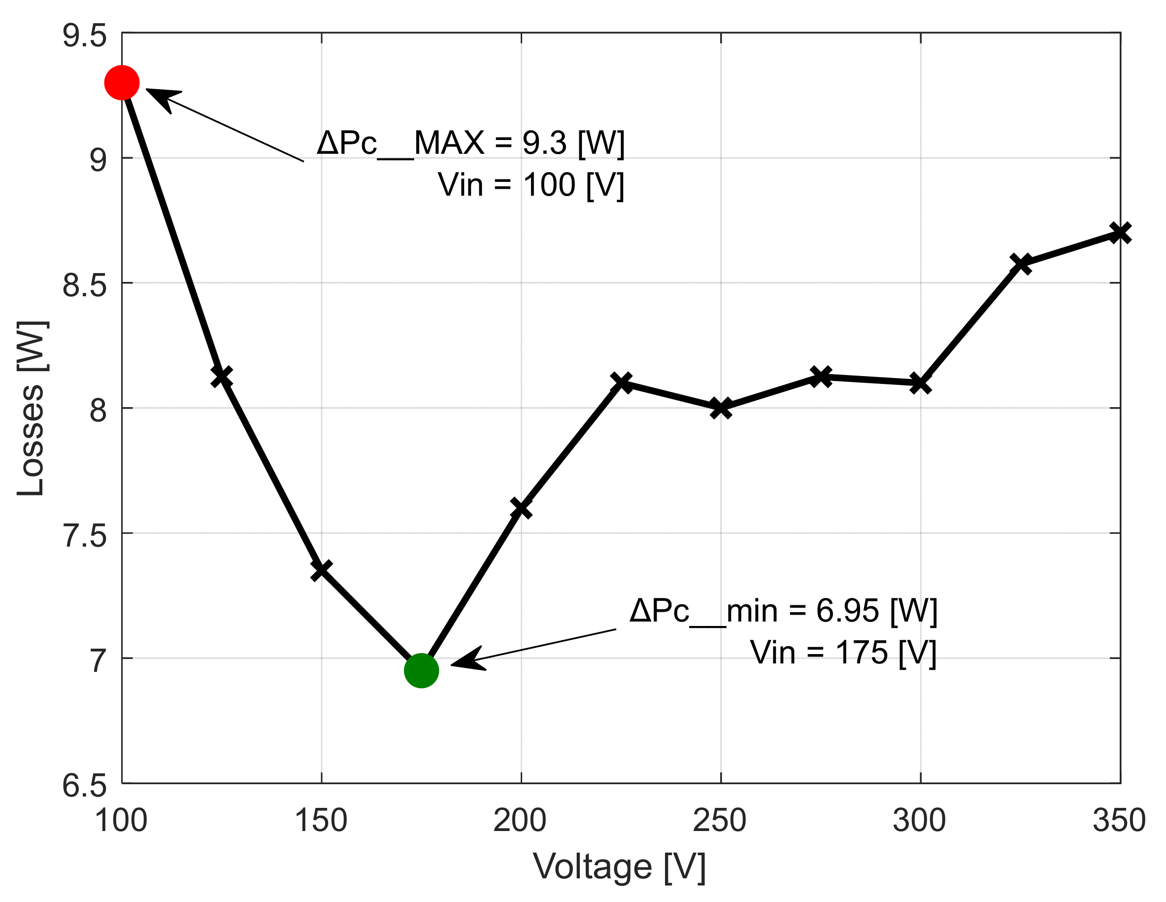
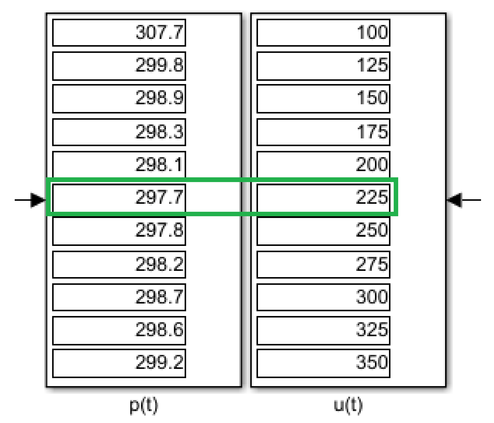
| 100 | 2.253 | 225.300 | 72.000 | 3.000 | 216.000 | 95.872 | 9.300 | 44.385 |
| 125 | 1.793 | 224.125 | 72.000 | 3.000 | 216.000 | 96.375 | 8.125 | 69.716 |
| 150 | 1.489 | 223.350 | 72.000 | 3.000 | 216.000 | 96.709 | 7.350 | 100.739 |
| 175 | 1.274 | 222.950 | 72.000 | 3.000 | 216.000 | 96.883 | 6.950 | 137.363 |
| 200 | 1.118 | 223.600 | 72.000 | 3.000 | 216.000 | 96.601 | 7.600 | 178.891 |
| 225 | 0.996 | 224.100 | 72.000 | 3.000 | 216.000 | 96.386 | 8.100 | 225.904 |
| 250 | 0.896 | 224.000 | 72.000 | 3.000 | 216.000 | 96.429 | 8.000 | 279.018 |
| 275 | 0.815 | 224.125 | 72.000 | 3.000 | 216.000 | 96.375 | 8.125 | 337.423 |
| 300 | 0.747 | 224.100 | 72.000 | 3.000 | 216.000 | 96.386 | 8.100 | 401.606 |
| 325 | 0.691 | 224.575 | 72.000 | 3.000 | 216.000 | 96.182 | 8.575 | 470.333 |
| 350 | 0.642 | 224.700 | 72.000 | 3.000 | 216.000 | 96.128 | 8.700 | 545.171 |
| Vin [V] | Iin [A] | Pin [W] | Vout [V] | Iout [A] | Pout [W] | η [%] | ΔPC [W] | Zin [Ω] |
|---|---|---|---|---|---|---|---|---|
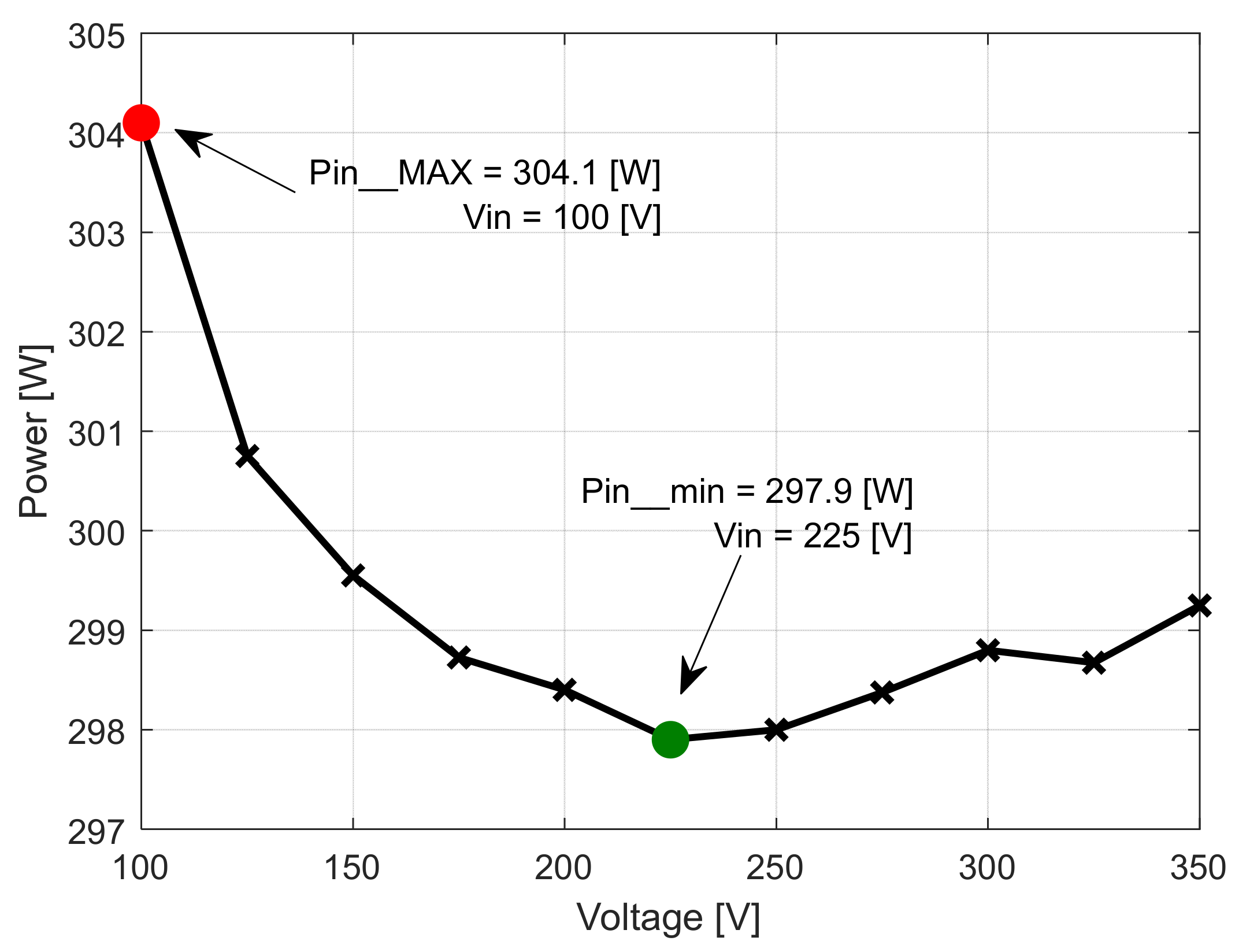
| 100 | 3.041 | 304.100 | 72.000 | 4.000 | 288.000 | 94.706 | 16.100 | 32.884 |
| 125 | 2.406 | 300.750 | 72.000 | 4.000 | 288.000 | 95.761 | 12.750 | 51.953 |
| 150 | 1.997 | 299.550 | 72.000 | 4.000 | 288.000 | 96.144 | 11.550 | 75.113 |
| 175 | 1.707 | 298.725 | 72.000 | 4.000 | 288.000 | 96.410 | 10.725 | 102.519 |
| 200 | 1.492 | 298.400 | 72.000 | 4.000 | 288.000 | 96.515 | 10.400 | 134.048 |
| 225 | 1.324 | 297.900 | 72.000 | 4.000 | 288.000 | 96.677 | 9.900 | 169.940 |
| 250 | 1.192 | 298.000 | 72.000 | 4.000 | 288.000 | 96.644 | 10.000 | 209.732 |
| 275 | 1.085 | 298.375 | 72.000 | 4.000 | 288.000 | 96.523 | 10.375 | 253.456 |
| 300 | 0.996 | 298.800 | 72.000 | 4.000 | 288.000 | 96.386 | 10.800 | 301.205 |
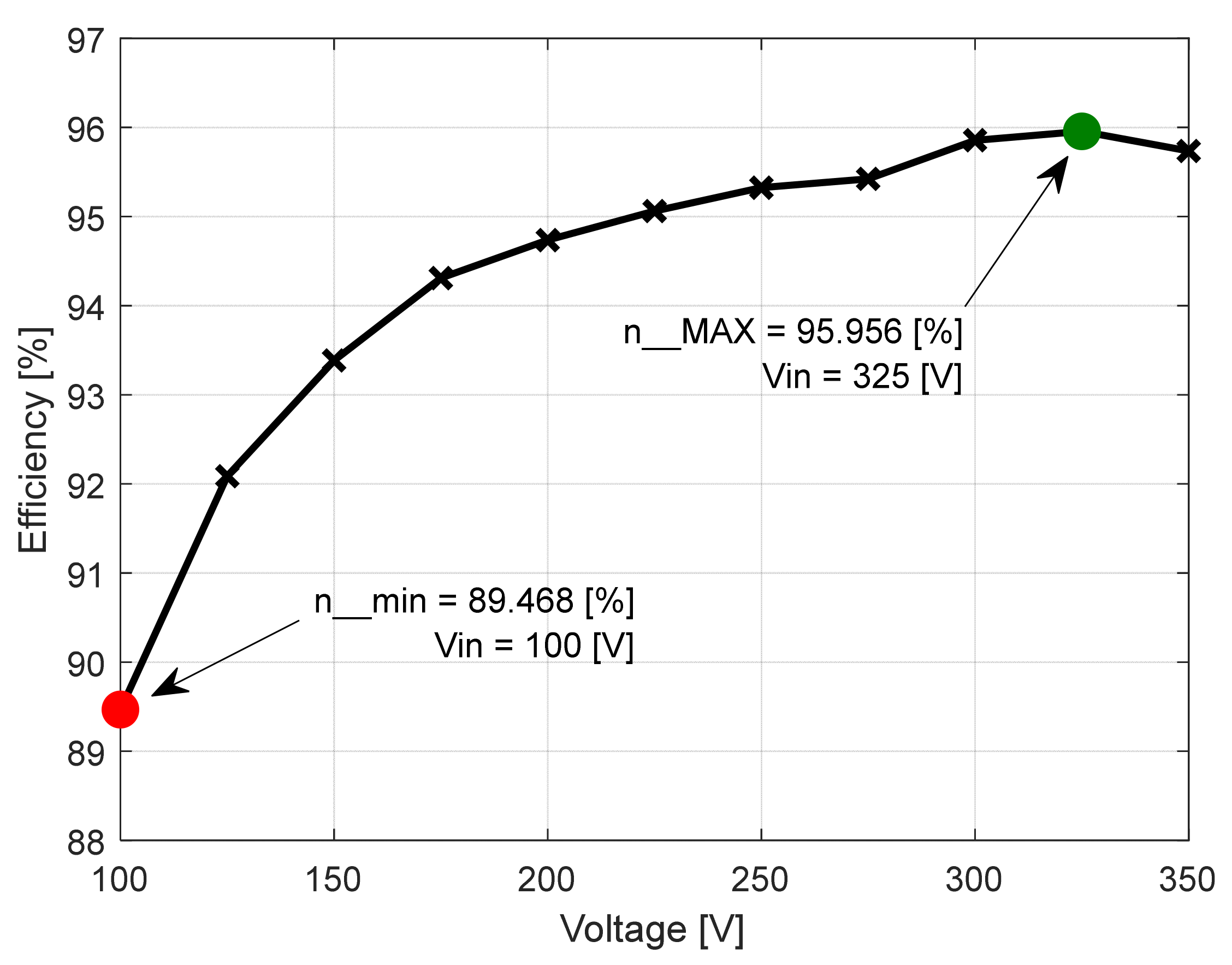
| 325 | 0.919 | 298.675 | 72.000 | 4.000 | 288.000 | 96.426 | 10.675 | 353.645 |
| 350 | 0.855 | 299.250 | 72.000 | 4.000 | 288.000 | 96.241 | 11.250 | 409.357 |
| Vin [V] | Iin [A] | Pin [W] | Vout [V] | Iout [A] | Pout [W] | η [%] | ΔPC [W] | Zin [Ω] |
|---|---|---|---|---|---|---|---|---|
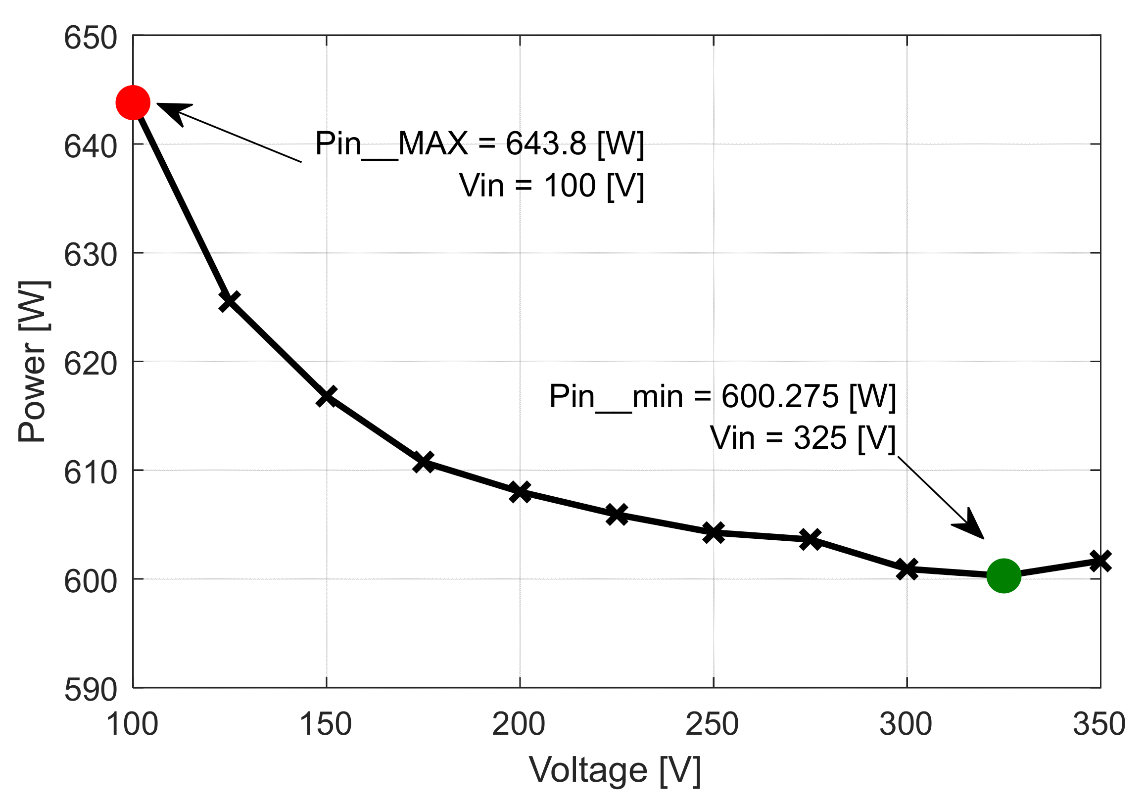
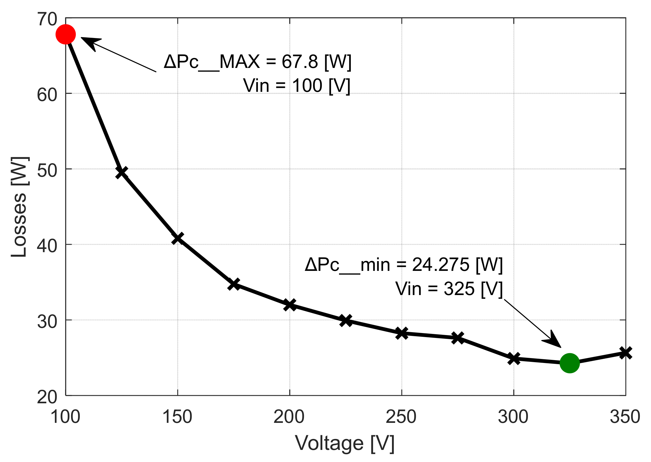
| 100 | 6.438 | 643.800 | 72.000 | 8.000 | 576.000 | 89.468 | 67.800 | 15.533 |
| 125 | 5.004 | 625.500 | 72.000 | 8.000 | 576.000 | 92.086 | 49.500 | 24.980 |
| 150 | 4.112 | 616.800 | 72.000 | 8.000 | 576.000 | 93.385 | 40.800 | 36.479 |
| 175 | 3.490 | 610.750 | 72.000 | 8.000 | 576.000 | 94.310 | 34.750 | 50.143 |
| 200 | 3.040 | 608.000 | 72.000 | 8.000 | 576.000 | 94.736 | 32.000 | 65.789 |
| 225 | 2.693 | 605.925 | 72.000 | 8.000 | 576.000 | 95.061 | 29.925 | 83.550 |
| 250 | 2.417 | 604.250 | 72.000 | 8.000 | 576.000 | 95.324 | 28.250 | 103.434 |
| 275 | 2.195 | 603.625 | 72.000 | 8.000 | 576.000 | 95.423 | 27.625 | 125.285 |
| 300 | 2.003 | 600.900 | 72.000 | 8.000 | 576.000 | 95.856 | 24.900 | 149.775 |
| 325 | 1.847 | 600.275 | 72.000 | 8.000 | 576.000 | 95.956 | 24.275 | 175.961 |
| 350 | 1.719 | 601.650 | 72.000 | 8.000 | 576.000 | 95.736 | 25.650 | 203.607 |
| Pout [W] | 72 | 144 | 216 | 288 | 360 | 432 | 504 | 576 | 648 | 720 | 792 |
|---|---|---|---|---|---|---|---|---|---|---|---|
| ΔηREC [%] | 3.294 | 1.252 | 1.011 | 1.971 | 3.236 | 4.318 | 5.423 | 6.488 | 7.867 | 8.804 | 9.822 |
| ΔPC_REC [W] | 2.55 | 1.925 | 2.35 | 6.2 | 12.925 | 21 | 31.3 | 43.525 | 61 | 77 | 96 |
Disclaimer/Publisher’s Note: The statements, opinions and data contained in all publications are solely those of the individual author(s) and contributor(s) and not of MDPI and/or the editor(s). MDPI and/or the editor(s) disclaim responsibility for any injury to people or property resulting from any ideas, methods, instructions or products referred to in the content. |
© 2023 by the authors. Licensee MDPI, Basel, Switzerland. This article is an open access article distributed under the terms and conditions of the Creative Commons Attribution (CC BY) license (https://creativecommons.org/licenses/by/4.0/).
Share and Cite
Pintilie, L.N.; Hedeșiu, H.C.; Rusu, C.G.; Teodosescu, P.D.; Mărginean, C.I.; Salcu, S.I.; Suciu, V.M.; Szekely, N.C.; Păcuraru, A.M. Energy Conversion Optimization Method in Nano-Grids Using Variable Supply Voltage Adjustment Strategy Based on a Novel Inverse Maximum Power Point Tracking Technique (iMPPT). Electricity 2023, 4, 277-308. https://doi.org/10.3390/electricity4040017
Pintilie LN, Hedeșiu HC, Rusu CG, Teodosescu PD, Mărginean CI, Salcu SI, Suciu VM, Szekely NC, Păcuraru AM. Energy Conversion Optimization Method in Nano-Grids Using Variable Supply Voltage Adjustment Strategy Based on a Novel Inverse Maximum Power Point Tracking Technique (iMPPT). Electricity. 2023; 4(4):277-308. https://doi.org/10.3390/electricity4040017
Chicago/Turabian StylePintilie, Lucian Nicolae, Horia Cornel Hedeșiu, Călin Gheorghe Rusu, Petre Dorel Teodosescu, Călin Ignat Mărginean, Sorin Ionuț Salcu, Vasile Mihai Suciu, Norbert Csaba Szekely, and Alexandru Mădălin Păcuraru. 2023. "Energy Conversion Optimization Method in Nano-Grids Using Variable Supply Voltage Adjustment Strategy Based on a Novel Inverse Maximum Power Point Tracking Technique (iMPPT)" Electricity 4, no. 4: 277-308. https://doi.org/10.3390/electricity4040017