Article

Efficient and Accurate Modeling of the Surface Deflection of Thin Layers on Composite Substrates with Applications to Piezoelectric Parameter Measurements

1
Institute for Microelectronics and Microsensors, Johannes Kepler University Linz, A-4040 Linz, Austria
2
Department for Integrated Sensor Systems, Danube University Krems, A-2700 Wiener Neustadt, Austria
3
Institute of Sensor and Actuator Systems, TU Wien, A-1040 Vienna, Austria
4
Shanghai Institute for Microsystem and Information Technology, Chinese Academy of Sciences, Shanghai 200050, China
*
Author to whom correspondence should be addressed.
Micro 2022, 2(3), 369-389; https://doi.org/10.3390/micro2030025
Submission received: 2 June 2022 / Revised: 23 June 2022 / Accepted: 27 June 2022 / Published: 29 June 2022

Abstract

:
The electrical and mechanical response of multilayered structures involving a piezoelectric layer and bull’s eye shaped electrodes is investigated. A boundary element method is employed based on spectral domain Green’s functions. With this method, the electric field distribution is determined first, and the local mechanical displacement in a second step. As will be shown, this allows us to exploit cylindrical symmetry for the electric surface charge distribution, but not for the vertical surface displacements. The effect of substrate bending due to in plane-stress, introduced by the piezoelectric constant d 31 , and the benefits of using bull’s eye electrode geometries with thick metallic backplates intended to reduce this effect are studied. A rigorous analysis and a largely simplified, but accurate approximation are compared. The application of this technique is demonstrated on a practical example for highly efficient and accurate determination of selected piezoelectric coefficients from surface topography measurements on such structures.

Graphical Abstract

1. Introduction

Laser optical measurements of the vertical displacement profile on grown piezoelectric films on silicon substrates is a common technique to determine the piezoelectric parameters of the deposited piezoelectric layer [1,2]. However, the relation between piezoelectric parameters and the measurement is not straightforward, so that a common approach is to gradually adjust the parameters of a finite element model to achieve agreement between simulation and measurement [3]. The cylindrical symmetry of circular- or bull’s eye-shaped electrode geometries on multilayered piezoelectric composites (see Figure 1) is commonly exploited to achieve numerically efficient finite element method (FEM) models of these structures. However, the justification for this simplification is not guaranteed by the geometry alone, but instead, depends also on whether the influence of anisotropy of the materials involved is negligible or not. As will be shown, the lateral anisotropy has a significant impact on the considered problem, and therefore a reduction to a symmetric representation in order to reduce complexity is not justified in general.
In this work, an efficient and accurate boundary integral technique based on spectral Green’s functions (i.e., wavenumber domain representations) is employed to model the transverse deflection of abovementioned structures. A similar approach has been extensively used in the past for modeling wave propagation in surface acoustic wave sensors [4,5,6,7]. Unfortunately, the implementation of the proposed method in its rigorous form requires a relatively high level of modeling effort, which the practitioner, who is mainly interested in the results, usually wants to avoid. Fortunately, the characteristic properties of such structures allow for a significant reduction in complexity such that an accurate and fast calculation can be obtained, which may also appeal to an end user. The simplified calculation has been reported in the authors’ earlier work [8] showing that the problem can be reduced to the determination of a spectral Green’s function and numerical integration. In this work, the rigorous calculation and the subsequent simplifications leading to the simplified form are shown. Researchers who are mainly interested in the application can therefore may skip the rigorous treatment in Section 2 and jump directly to the reduced form in Section 5.

2. Basic Modeling Approach

The modeling approach in this work uses a boundary element method (BEM) implemented in the wavenumber domain based on Green’s functions (GF) that is similar to the method discussed in [9]. It can be summarized as follows: we use two Green’s functions G φ and G u , where the indices φ and u refer the electric potential and the mechanical displacement, respectively. G φ relates electrode charge distribution and potential and is used to determine the electric charge for a prescribed electrode potential. The mechanical displacement is calculated based on the charge distribution using G u . Interesting properties of the problem can readily be investigated by closer inspection of the Green’s functions (see Section 2.1 below). For instance, whether a reduction to circular symmetry is permissible or not is most easily determined. Furthermore, the decay lengths of the fields, and thus the influence of the vertical extension of the modeling domain, e.g., the air half-space above the electrodes, and the material thicknesses can be estimated and may provide useful information and benchmarks for the developers of FEM simulation models as well.
The Green’s functions used are specified in the spectral domain, to take into account the time-harmonic measurement mode of the laser Doppler vibrometer used to record the deflection. The method is therefore inherently dynamic, and it can be directly observed in the GF at which oscillation frequencies wave propagation phenomena will occur. Dispersion relations are shown in Section 2.1 revealing that Lamb-type waves exist that have no cut-off frequency, and must be suppressed by limiting the radial extension of the structure clearly below the critical wavelength, in order to avoid interference. A closer examination of the GF in the next section also discloses if the oscillation frequency in an experiment considered quasistatic is sufficiently low, or if a static model must be replaced by a dynamic one.

2.1. Green’s Functions

2.1.1. Symmetry Considerations

Some of the basic features of Green’s functions will be discussed before they are treated in detail in Section 3.1. The symmetry properties of the GF indicated in Figure 2 will be used to simplify the calculations in advance. For laterally ( x 1 , x 2 ) infinitely extended and homogeneous layers, the GF are shift invariant in the x 1 / x 2 plane, i.e., G ( r , r ) = G ( Δ r ) , with Δ r = r r and r = x 1 e x 1 + x 2 e x 2 . Here, r , r , and e i are the vector to the field point, the vector to the source point, and the unity vectors in i-direction, respectively. For cylindrical symmetry, G ( Δ r ) = G [ | Δ r | cos ( ϕ ) e x 1 + | Δ r | sin ( ϕ ) e x 2 ] is required, or equivalently G ˜ ( k ) = G ˜ [ | k | cos ( ψ ) e k 1 + | k | sin ( ψ ) e k 2 ] in the spectral domain, where ϕ and ψ are the azimuthal angle in the spatial and wave domain, respectively. In the remainder of this paper, spectral domain quantities are marked with a tilde symbol ˜. The calculation of the GF is performed in the wavenumber ( k 1 , k 2 ) domain, with details given in [5,9,10], for instance, where k is the wave vector and k i its components in e k i directions, respectively. Results are shown for electrostatic G ˜ φ ( k ) and the mechanical GF G ˜ u ( k ) . The key results are that anisotropy, boundary conditions, and layer thicknesses influence G ˜ φ and G ˜ u differently, allowing certain simplifications to be applied. These results may also be beneficial for developers of finite element models in order to check for reduction in complexity without impairing validity or accuracy. The spectral electrostatic GF G ˜ φ ( k ) is shown in Figure 2 (left), where only negligible dependence on the angle ψ is observed. On the contrary, a noticeable change over ψ is visible for the electromechanical GF G ˜ u ( k ) . Therefore, a simplification to radial symmetry is only valid for the calculation of the electrical fields, but not for the mechanical displacement.

2.1.2. Dispersion Relations

The vertical displacement of the in the x 1 / x 2 -plane infinitely extended layer composite due to a surface charge distribution ρ ˜ at its top is given by
u ˜ z ( k ) = G ˜ u ( k ) ρ ˜ ( k )
in the spectral domain. At certain critical wavevectors k * ( ω ) , G ˜ u [ k * ( ω ) ] shows poles indicating that a wave propagating in k direction is possible, even for vanishing electrical excitation. The associated critical wavelengths λ * and phase velocities v * are given by
λ * = 2 π / | k * ( ω ) | , v * = ω / | k * ( ω ) | .
The dispersions of critical wavelengths for different aluminum backplane thicknesses are shown in Figure 3. It can be observed that at frequencies as low as 1 Hz, the critical wavelengths are very long and in the order of meters for the anti-symmetric Lamb wave. In case of high frequency operation and larger extended substrates, interference due to standing waves has to be considered. Although the dispersion is dominated by the aluminum plate, it varies considerably from the well known dispersion diagram of single aluminum plates (see, e.g., [11]), which can be attributed to the additional layers. The symmetric mode with its extraordinarily long wavelength ( λ 5.8 m at f = 1 kHz) is not considered, as the limited extension of the structure does not support these waves. Therefore, from G ˜ u , it can already be determined if standing wave interference will be of concern in the measurement setup.

2.2. Boundary Element Method

Defined piecewise constant electric potentials of φ ( r ) of 1 V and 1 V are applied to the central and outer ring electrodes, respectively, while the aluminum backplane is grounded (0 V). The resulting electric charge distribution induces mechanical displacements of the piezoelectric AlN film and the non-piezoelectric underlying layers. In the first step, the resulting surface charge distribution on the electrodes ρ ( r ) is determined by the method of mean weighted residuals. In a second step, the displacement field in out-of-plane direction u z ( r ) is calculated.

2.2.1. Method of Mean Weighted Residuals (MWR)

The method of MWR can be summarized as following [9]: the potential φ ˜ ( k ) and the surface charge density ρ ˜ ( k ) are directly related by the spectral electrostatic Green’s function G ˜ φ ( k ) in the wavenumber (k) domain
φ ˜ ( k ) = G ˜ φ ( k ) ρ ˜ ( k )
with k representing the radial wavenumber k 2 = k 1 2 + k 2 2 for the radially symmetric fields. The transformation to the spatial domain (with spatial radial coordinate r) is obtained by inverse Hankel transform (A scaling factor of 1 / ( 2 π ) has been introduced for agreement with the two dimensional inverse Fourier transform of radially symmetric functions).
φ ( r ) = 1 2 π 0 G ˜ φ ( k ) ρ ˜ ( k ) J 0 ( k r ) k d k ,
where J n ( · ) denote in the following Bessel functions of the first kind and n th order. The charge distribution is synthesized by an infinite series of trial functions B i ( r ) scaled by factors a i
ρ ( r ) = i = 0 a i B i ( r ) , ρ ˜ ( k ) = i = 0 a i B ˜ i ( k )
in the spatial and spectral domain. The residuals are weighted with functions T j ( r ) · r according to
0 T j ( r ) φ ( r ) r d r = i = 0 a i 0 G ˜ φ ( k ) B ˜ i ( k ) T ˜ j ( k ) k d k .
For convenience, such integrals can be shortened as an inner product
T j , φ = i = 0 G ˜ φ , B ˜ i T ˜ j a i ,
with a distinction between spatial an spectral integrals according to
b j = T j , φ = 0 T j ( r ) φ ( r ) r d r ,
M i j = G ˜ φ , B ˜ i T ˜ j = 0 G ˜ φ ( k ) B ˜ i ( k ) T ˜ j ( k ) k d k .
From (6)–(9), a linear system
b j = M i j a i ,
or in matrix notation
b = M · a ,
for the unknown coefficients a i of the series expansion (5) arises.

2.2.2. Displacement Field Calculation

Once the coefficients a i are calculated, the charge distribution follows from (5) in both domains. The vertical displacement u z can subsequently be derived from [7]
u z ( r , ϕ ) = 1 4 π 2 i = 0 a i 0 B ˜ i ( k ) k 0 2 π G ˜ u ( k , ψ ) e j k r   cos ( ϕ ψ ) d ψ d k ,
where G ˜ u ( k , ψ ) denotes a spectral Green’s function relating mechanical displacement and surface charge density, which is in contrast to G ˜ φ ( k ) not symmetric as it varies with the angle ψ as previously illustrated in Figure 2.

3. Application

The basic approach outlined in Section 2 is now applied to the particular problem of the layered structure depicted in Figure 1. The respective material parameters of the layers used for calculation are summarized in Appendix A.1. The explicit derivation of the Green’s function is, e.g., collected in [12,13]. First, the construction of the Green’s function and an approximation for G ˜ φ based on a non-piezoelectric material are shown. The integrals in (8) and (9) are computed using a finite number of rectangular basis and weighting functions for which closed-form solutions are available. Therefore, very thin elements, for which the integrals converge only very slowly, can be calculated in closed form, such that the elements can be refined at the electrode edges where gradients are largest. The purpose of this rather cumbersome approach is to have an exact solution at hand to validate the applicability of simplifications. For example, it will be shown that the calculation of the charge distribution using the MWR approach can be avoided at all for the practical thicknesses of piezoelectric AlN layers typically in the range of a few hundreds on nanometers. A very efficient calculation requiring only the evaluation of one Green’s functions and direct numerical integration can be obtained.

3.1. Electrostatic Green’s Function

The crucial part of this method is the accurate knowledge of the Green’s functions. Unfortunately, a closed form expression for the electrostatic Green’s function considering all material layers yields a too complex function for direct analytical integration. Fortunately, the high conductivity of the comparably thick doped silicon layer leads to a strong concentration of the electrical field within the piezoelectric layer and thus only negligible electrical influence of the layer composition below the piezoelectric layer results. However, the dominant electric field in thickness direction and the non-zero piezoelectric stress constant e 31 , e 32 , or equivalently non-zero piezoelectric constants d 31 , d 32 produce shear stresses on the silicon surface and thus influence G ˜ φ ( k ) noticeably. Our approach is therefore to consider the AlN layer alone and to neglect mechanical loading effects for the moment and account for it later by adjusting the parameters of the approximate model.
According to the IEEE standard on piezoelectricity [14], the two equivalent sets of constitutive piezoelectric equations in Voigt notation [15] are the stress-charge form
T = c E : S e · E , D = e : S + ε S · E ,
and the strain-charge form
S = s E : T + d · E , D = d : T + ε T · E .
They can be converted to each other using the relations
c E = ( s E ) 1 ,
ε S = ε T d : ( s E ) 1 : d ,
e = ( s E ) 1 : d .
Here, T , S , c , s , ε , E and D , are the tensors of stress, strain, elastic stiffness, compliance, permittivity the vectors of the electric field strength and the electric displacement, respectively. In addition, d and e refer to as the piezoelectric tensor in strain-charge and stress-charge form, respectively. Conversion between both systems is regularly required because the calculation of Green’s function, e.g., in [12] is performed using (13), whereas piezoelectric materials are mostly characterized by the parameters of (14). The material tensors of AlN (wurtzite, class 6 mm, see, e.g., pp. 300 in [16]) are given by (Note that the structures of the material tensors in system (13) are equal to (14) for this class).
c E = c 11 E c 12 E c 13 E 0 0 0 c 11 E c 13 E 0 0 0 c 33 E 0 0 0 s c 44 E 0 0 y c 44 E 0 m c 66 E
e = 0 0 0 0 e 15 0 0 0 0 e 15 0 0 e 31 e 31 e 33 0 0 0 ,
ε S = ε 11 S 0 0 0 ε 11 S 0 0 0 ε 33 S .
The representation (14) is more suitable in the stress free case T = 0 , and G ˜ φ can be calculated from D = ε T · φ and · D = 0 with respective boundary conditions, yielding
G ˜ φ ( k ) = 1 k 1 ε 0 f ( h I , k ) + ε eff coth ( h II k ε 33 T / ε 11 T ) with ε eff = ε 11 T ε 33 T .
This result is very similar to the GF for isotropic materials as can be found, e.g., in [17]. The function f ( h I , k ) accounts for the extension of the air domain (I) with different boundary conditions at h I
f ( h I , k ) = 1 air halfspace coth ( h I k ) conductor at h I tanh ( h I k ) zero charge at h I .
Infinite air halfspaces are easily implemented by the BEM. However, for FEM models, where the air domain has to be discretized in a vertical direction, the required extension is of interest and can be approximated with the following consideration. For a disk of radius R, the lowest dominant wavenumber is k 2 π / ( 4 R ) and the hyperbolic functions are approximately 1 at h I k = π . Therefore, it is advised to use h I > 2 R .
The stress free solution in (21) is exact for d = 0 pm/V (or e = 0 C/m 2 ). Deviations due to piezoelectricity can be well approximated by adjusting the ε 11 T and ε 33 T parameters to a certain extent as shown in Figure 4. For curve (1), the properties of bulk AlN ( d 15 = d 24 = 2.5 , d 31 = 2.1 , d 33 = 5.2 pm/V) are used and the adjustment yields excellent agreement. This is also the case when only d 33 is active as shown in curve (2) ( d 15 = d 24 = d 31 = 0 pm / V , d 33 = 20 pm/V). The sensitivity to d 33 is relatively weak, but the results change significantly when d 31 becomes larger as shown in curve (3), where d 15 = d 24 = d 33 = 0 pm/V and d 31 = 4 pm/V is set. In curve (4), d 15 = d 24 = 2.5 pm/V, d 31 = 5 pm/V and d 33 = 16 pm/V is shown. It can therefore be concluded that approximations in closed form are possible. For strong piezoelectric coupling, the agreement suffers at low wavenumbers, but the asymptotic behavior as k is always accurately reproduced, which is a crucial property as it allows an efficient implementation of the BEM in (6), which is discussed in the following section.

3.2. Calculation of the Electric Field Using MWR

The field calculation in cylindrical symmetry always requires the calculation of integrals with strongly oscillating kernels. As shown in Figure 4, G ˜ φ decays slowly (dominated by k 1 according to (21)) such that a numerical computation of the integral
0 T ˜ j ( r ) φ ( r ) r d r = i = 0 a i 0 G ˜ φ ( k ) B ˜ i ( k ) T ˜ j ( k ) k d k
is exhaustive. In order to achieve a numerically efficient implementation, our approach is to use simple trial B ˜ i ( k ) and weighting functions T ˜ j ( k ) , which allow us to use closed form expressions for the infinite integrals. An alternative approach is to use specialized orthogonal functions that already approximate the expected charge distribution reasonably, such that a lower number of trial functions yield good results, but involves complicated integrals. For instance, this approach is used by [18] to formulate the problem as dual integral equations and solved using techniques, e.g., found in [19]. An interesting feature of our presented approach is that when the trial functions of [18] are used and the weighting functions T ˜ j ( k ) are set equal to the trial functions B ˜ i ( k ) , then (6) yields the same integral and solution system as presented in [18]. The approach presented in this paper is therefore equivalent to the dual integral approach.
In the following, we use the first method with simple non-overlapping hollow cylindrical trial and weighting functions centered at the radii r i , j with wall thickness w i , j , shown in Figure 5 for which the integrals can be computed in closed form. The spectral domain representations are obtained by Hankel transform by
B ˜ i ( k ) = 1 k α i J 1 k α i β i J 1 k β i ,
T ˜ j ( k ) = 1 k α j J 1 k α j β j J 1 k β j ,
with
α i , j = r i , j + w i , j / 2 , β i , j = r i , j + w i , j / 2 .
G ˜ φ can also be expanded into an infinite series of exponentials
G ˜ φ = a 1 k 1 + n = 1 g n exp ( n a 3 k )
with
a 1 = 1 ε 0 + ε eff , a 2 = 2 ε eff ε eff ε 0 ,
a 3 = 2 h II ε 33 T / ε 11 T , g n = ( 1 ) n a 2 ( a 2 1 ) n .
The right-hand-side of (6) can be represented by a sum of four so-called Lipschitz–Hankel integrals I ( μ , ν ; λ ) defined by (A1) of the type type I ( 1 , 1 ; 2 ) [20]
0 a 1 k 2 1 + n = 1 g n exp ( n a 3 k ) J 1 ( k α ) J 1 ( k β ) d k .
According to page 389 in [21] or page 315 in [22], the improper integral on the left side of (30) with highly oscillating kernel can be replaced by the finite integral over a smooth function stated in the right side of (30)
0 1 k 2 exp ( x k ) J 1 ( k α ) J 1 ( k β ) d k = 1 π 0 π α β sin 2 ( ϕ ) x + x 2 + α 2 + β 2 2 α β cos ( ϕ ) d ϕ
that can be efficiently evaluated. Moreover, this integral can be expressed in closed form by means of elliptic integrals. To the best of the authors’ knowledge, it is not straight-forward to find this representation in the common literature on integrals. It is therefore derived in the Appendix. Efficient implementations for elliptic integrals are reported in [23] and are made available for MATLAB, e.g., by T. Hoffend [24]. The sum in (29) converges for b > 2 , which is always given. The amount of summands required to achieve a relative accuracy of f can be estimated by N = log ( f ) / log ( a 2 1 ) and is larger for piezoelectric materials with high permittivity (see (27)). By using the convergence acceleration method for alternating series of Longman [25], N can be drastically reduced while retaining high numerical accuracy. For the calculation of the expansion coefficients a i , the matrix M in (10) has to be evaluated for all j and i first, using the right-hand-side integral in (6). The charge distribution is calculated using a truncated version of (5)
a = M 1 · b , ρ ( r ) i = 0 N a i B i ( r ) .
The symmetric matrix M summarizes the various interactions between potentials at segments r j and surface charge at r i . The mutual influence of the elements decreases with distance | r j r i | , i.e., the self action contributions at the diagonal are dominant. For piezoelectric layers being thin compared to the element width w i , j , this decrease is stronger, and it is sufficient to calculate only a limited amount of upper diagonals of M and use the symmetry property. In Figure 6 and Figure 7, the resulting surface charge densities and the respective electrical potentials for different thicknesses h II of 0.5 μ m, 5 μ m, and 50 μ m of the piezoelectric layers are shown for the inner and outer electrode. It is observed that the charge distribution is nearly uniformly distributed and the charge accumulations at the electrode edges are not dominant for the 500 nm thick AlN layer used in the later shown experiment. This picture changes for thicker layers, especially when the thickness is comparable to the radii of the electrodes. Figure 6 also shows the simple approximation for constant charge densities and the simulated ( C i , C o ) and approximated ( C ^ o , C ^ i ) capacitances of the inner and outer electrodes calculated by
C i = 2 π φ i 0 R i ρ ( r ) r d r , C o = 2 π φ o R o 1 R o 2 ρ ( r ) r d r ,
C ^ i = ε eff R i 2 π / h II , C ^ o = ε eff ( R o 2 2 R o 1 2 ) π / h II .
This further substantiates the validity of approximating the charge densities as constant over each electrode, when applying thin AlN layers.

3.3. Calculation of the Displacement Field

The displacement field can be calculated using (12), but the computation of the integral is inconvenient. Expanding the ψ -dependence into a Fourier series ( G ˜ u ( k , ψ ) is 2 π -periodic in ψ ) yields
G ˜ u ( k , ψ ) = n = G ˜ u , n ( k ) e j n ψ .
Using the identity
0 2 π e j k r   cos ( ϕ ψ ) e j n ψ d ψ = 2 π e j n ( ϕ π / 2 ) J n ( k r )
valid for integer n, the integral in (12) can be replaced by
u z ( r , ϕ ) = 1 2 π n = e j n ( ϕ π / 2 ) i = 0 a i 0 B ˜ i ( k ) k G ˜ u , n ( k ) J n ( k r ) d k .
In Figure 8, G ˜ u ( k , ψ ) over ψ is shown for some wavenumbers k. It can be observed that the variation over ψ can be approximated by a single cosine function with period 4, and therefore a good approximation is found with (Note that G ˜ u , 4 = G ˜ u , 4 and J n ( x ) = ( 1 ) n J n ( x ) for integer n).
G ˜ u ( k , ψ ) = G ˜ u , 0 ( k ) + 2 G ˜ u , 4 ( k ) cos ( 4 ψ ) .
The approximate mechanical displacement field follows from
u z ( r , ϕ ) = 1 2 π i = 0 a i ( 0 B ˜ i ( k ) k ( G ˜ u , 0 ( k ) J 0 ( k r ) + 2 cos ( 4 ϕ ) G ˜ u , 4 ( k ) J 4 ( k r ) ) d k ) .
The evaluation of this integral is still difficult because of the oscillatory behavior of the integrand. Again, an approximation for the asymptotic behavior of G ˜ u that can be integrated is crucial for efficient numerical evaluation. In Figure 9, G ˜ u is shown at low (left) and high (right) wavenumbers. At low wavenumbers, G ˜ u depends strongly on the thickness of the aluminum layer (IV). On the contrary, at high wavenumbers, this dependence is not noticeable and an approximation using damped exponential functions
G ˜ u , 0 ( k ) = 1 k i = A i e k δ i + j k w i
is possible, where δ i denotes the damping factor. The assocatated parameters can be determined using Prony’s method [26]. For example, the function in Figure 9 (right) can be well approximated by using only the three terms ( i 1 , 0 , 1 ) of (39), i.e.,
G ˜ u , 0 ( k ) a 0 k [ 1 ( 1 / 2 + a 1 ) e ( δ + j w ) k ( 1 / 2 a 1 ) e ( δ j w ) k ] a 0 = 24.448 · 10 3 m 3 / As , a 1 = 1.0213 , w = 0.6995 · 10 6 m , δ = 1.4812 · 10 6 m ,
which is indicated in Figure 9 by the dashed line. By using this approximation and the trial functions in (23) for the calculation of the vertical displacement, integrals of type I ( 0 , 1 , 1 ) of the Lipschitz–Hankel integrals (see (A1) in the Appendix) are encountered. Their conversion to well behaved functions for efficient numerical evaluation is stated in the Appendix. The function G ˜ u , 4 is shown in Figure 10. The spectral decay rate is in the order of k 12 , i.e., for this function, integrals of I ( 1 , 4 , 12 ) must be evaluated. A conversion to smooth integrals according to [22] is only possible for I ( 1 , 4 , λ ) with λ > 4 , however, the original integral itself is already smooth enough for direct numerical integration using either the Romberg rule or by considering the method proposed in [27].

4. Results

The strong influence of d 13 on surface bending is best demonstrated by setting d 13 = 0 first. The vertical surface deflection is calculated using (38) and is shown in Figure 11 for different thicknesses of the AlN layer. The total deflection u z is dominated by d 33 and can be approximated by
u z = d 33 V
for thin layers. Noticeable deviations occur only at thicker layers. No substrate bending occurs, and therefore the lateral extension of the structure is not critical.
However, the picture changes if d 13 is active and significant surface bending due to in-plane stress is introduced (see Figure 12). The substrate bending of the structure is dominated by the behavior of G ˜ u at low wavenumbers and depends strongly on the thickness of the aluminum plate if the plate is below a certain thickness, as can be observed in Figure 9. Above a thickness of h IV = 2 mm, no significant change results for thicker plates. The propagation of the Lamb waves does only interfere noticeably for structures, which are laterally wider than the critical wavelengths shown in Figure 3. For the calculation of u z ( r ) , the integration of G ˜ u , 0 is split into two parts. For the asymptotic behavior at high wavenumbers, the approximation obtained by Prony’s method with subsequent least squares optimization given in (40) is used. The residual part of G ˜ u , 0 decays rapidly and can be evaluated accurately by straightforward numerical integration.

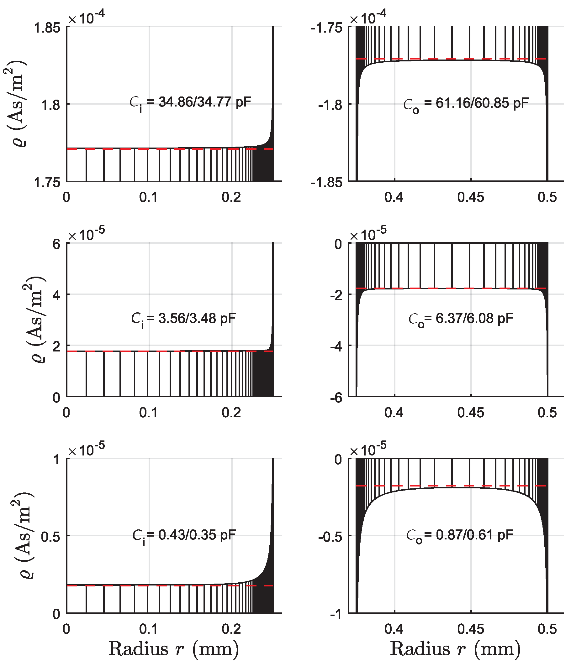
The Influence of the Radial Boundary Condition

In order to study the influence of the lateral extension of the structure when d 13 is active, a zero normal displacement u z = 0 at certain radii R c ( R c larger than the outer electrode, but lower than the critical wavelength λ * ) is enforced by using a dyadic Green function with additional surface force f ˜ z influence functions H ˜ u and H ˜ φ :
φ ˜ u ˜ z = G ˜ φ H ˜ φ G ˜ u H ˜ u · ϱ ˜ f ˜ z
The surface force densities are discretized using trial functions D n ( r ) with spectral representation D ˜ n ( k ) according to
f ˜ z ( k ) = m = 0 c k D ˜ n ( k ) .
The anisotropy of the structure is neglected in this case, and therefore the results are approximations which show the qualitative influence of fixed displacement at an outer ring. Instead of the system (10) given by b = M · a , the new system
b d = M N O P · a c
must be solved with additional unknown expansion coefficients c . The components of the additional matrix elements are given by
d n = u z , D n , N i n = G ˜ u , B ˜ i D ˜ n ,
O m j = H ˜ φ , D ˜ m B ˜ j , P m n = H ˜ u , D ˜ m D ˜ n .
The system (44) can be rearranged yielding the unknown coefficients a and c . An additional displacement contribution to the integral (38) as a result of the forces required to maintain zero displacement at the substrate edges results in the form of
u z , f ( r ) = 1 2 π n = 0 c n 0 D ˜ n ( k ) H ˜ u ( k ) J 0 ( k r ) k d k .
Figure 13 shows the effect of such boundary conditions. The dashed lines represent the required force distribution (100 rectangular elements each). For better visibility of the effects, the displacement at the disk center is subtracted for each simulation. It can be observed that the effect of the lateral boundary condition on the actual shape in the electrode region is hardly noticeable, but an offset depending on R c occurs. It is therefore concluded that the resulting displacement fields are not sensitive to the lateral boundary conditions. This simplifies the calculation considerably, especially when anisotropy is implemented. The effect of anisotropy for a pinned boundary condition at R c = 1.5 mm is shown in Figure 12 at an azimuth ϕ = 0 .

5. Efficient Calculation for Thin Layers

The charge distributions in Figure 6 are nearly constant and their magnitude can be estimated using ε eff . At the electrode edges, charges accumulate, but their impact is small for thin AlN layers. It can therefore be assumed that the charge distribution can be specified as known as long as the edge charges have no significant impact on surface bending. The spatial influence of a circular charge singularity is shown in Figure 14 and shows that the charge singularities act in a very limited range on the surface bending and can therefore be neglected. The charge distribution can therefore be estimated in advance, and the calculation of the MWR can be reduced to the evaluation of the integral in (36) with one trial functions for inner and outer electrode each. A further simplification is achieved when the infinite integral over the wavenumber is replaced by a Fourier-Bessel series [28]
u z ( r , ϕ ) = m = e j m ϕ π / 2 i = 0 a i ( n = 1 B ˜ i ( k m , n ) G ˜ u , m ( k m , n ) J m k m , n r f m , n ) ,
f m , n = 2 R c 2 J m + 1 ( η m , n ) 2 ,
k m , n = η m , n R c ,
where η m , n represents the m th zero of J n ( x ) .
Considering only the 0th and 4th order of G ˜ u and assuming piecewise constant charge distributions, the calculation can be approximated by k n = k 0 , n and k m = k 4 , m resulting in
u z ( r , ϕ ) π R c ( n = 1 N Λ ( k n ) G ˜ u , 0 ( k n ) J 0 ( k n r ) + cos ( 4 ϕ ) m = 1 M Λ ( k m ) G ˜ u , 4 ( k m ) J 4 ( k m r ) ) ,
Λ ( k ) = ρ i R i J 1 ( k R i ) + ρ o ( R o J 1 ( k R o ) R m J 1 ( k R m ) ) ,
ρ i , o = ± V ε eff / h II .
In Figure 15 simulation results using the described method are compared to measurements reported in [3], where the same structure was analyzed. From the measured raw data, an offset of 1.4 pm was subtracted. This offset has shown to be random for repeated scans. In this simulation, the results are very sensitive to the d 31 component, and a small modification from 2.1 to 2.128 pm/V results in good agreement between measurement and simulation. For the rigorous computation, the electric charge distribution was determined using the mean weighted residual approach. However, as was demonstrated, the numerically costly charge calculation can be avoided by approximating it using the effective dielectric constant of the AlN layer. This is permissibly due to the comparably high electrical conductivity of the n-doped silicon wafer (≈2 mS/m), which confines the electrical fields to the thin AlN layer at low oscillation frequencies. It is furthermore shown, that the radial mechanical boundary condition (e.g., a clamping at a certain radius) has, apart from causing an offset in vertical direction, negligible influence on the vertical displacements in the electrode regions.

6. Conclusions

The effect of the piezoelectric constant d 31 on the surface deflection and the insensitivity to the lateral boundary condition could be shown. In absence of d 31 and for thin layers up to some microns, the electric and the mechanical field distributions follow the one-dimensional results very closely, i. e., ρ ε eff / h II V and u z d 33 V . The influence of d 31 introduces a lateral stress, which deflects the surface in an anisotropic way, although the electric fields maintain their rotational symmetry. Simulations with neglected anisotropy may show noticeable deviations, especially at the outer electrode of the bull’s eye structure. The implementation of the anisotropy is relatively simple, due to the strong spectral decrease of the Fourier coefficients in azimuthal direction. The use of the aluminum backplane to reduce the effect of surface bending has shown to be clearly beneficial. It could also be demonstrated by analyzing the Green’s functions, that when a certain thickness is reached (in our case 2 mm), surface bending could not be reduced by a further increase of the backplane thickness h IV . From the Green’s functions, the symmetric and anti-symmetric Lamb-type waves can also be determined. It is concluded that the antisymmetric mode may interfere with the measurement at frequencies above hundreds of Hertz and for thin backplanes.

Author Contributions

Conceptualization, T.V.-B.; methodology, T.V.-B. and R.B.; software, T.V.-B.; validation, T.V.-B. and R.B.; formal analysis, T.V.-B.; investigation, T.V.-B.; resources, B.J., U.S. and T.S.; data curation, T.V.-B.; writing—original draft preparation, T.V.-B.; writing—review and editing, R.B., B.J. and U.S.; visualization, T.V.-B.; supervision, B.J. and T.S.; project administration, B.J., U.S. and T.S.; funding acquisition, B.J., T.S., T.Y. and X.O. All authors have read and agreed to the published version of the manuscript.

Funding

This research was supported by Linz Center of Mechatronics (LCM) in the framework of the Austrian COMET-K2 programme. This work has been conducted in part in the course of the research project “H-iSlice” funded by the Austrian Research Promotion Agency (FFG) under grant number 869181.

Conflicts of Interest

The authors declare no conflict of interest.

Appendix A

Appendix A.1. Summary of Applied Material Parameters

Appendix A.1.1. Silicon Substrate

elastic stiffness ( GPa ) : c 11 = c 22 = c 33 = 166 , c 12 = c 13 = c 23 = 64 , c 44 = c 55 = c 66 = 79.6 permittivity ( F / m ) : ε 11 = ε 22 = ε 33 = 11.9 ε 0 , density : ρ = 2329 kg / m 3 conductivity : σ = 2 mS / m

Appendix A.1.2. Aluminum Nitride

elastic stiffness ( GPa ) : c 11 E = c 22 E = 380 , c 33 E = 357 , c 44 E = c 55 E = 112 , c 66 E = 127.4 , c 12 E = 125 , c 13 E = c 23 E = 93.7 , piezoelectric constants ( pm / V ) : d 31 = d 32 = 2.1 , d 33 = 5.2 , d 24 = d 15 = 2.5 , permittivity ( F / m ) : ε 11 S = ε 22 S = ε 33 S = 9.2 · ε 0 density : ρ = 3260 kg / m 3

Appendix A.1.3. Aluminum (Isotropic Elasticity)

Young s modulus Y , Poisson s number , ν Y = 70 GPa , ν = 0.33 , ρ = 2700 kg / m 3 , σ = 37.7 MS / m

Appendix A.2. Identities for Lipschitz-Hankel Integrals

The considered Lipschitz–Hankel integrals with highly oscillating integrands are defined by [20]
I ( μ , ν ; λ ) : = 0 k λ exp ( x k ) J μ ( α k ) J ν ( β k ) d k
and can, according to [22] (p. 315 for I ( 1 , 0 ; 1 ) and [21] (p. 389 for I ( 1 , 1 ; 2 ) , be replaced by finite integrals over smooth functions. The integral for I ( 1 , 1 ; 2 ) can also be converted into a representation using the elliptic integrals defined in Appendix A.3 for highly efficient numerical computation.
I ( 1 , 1 ; 2 ) = 1 π 0 π α β sin 2 ( θ ) x [ 1 + 1 + γ ( θ ) ] d θ = a 0 + a 1 E 0 ( m ) + a 2 K 0 ( m ) + a 3 Π 0 ( l , m ) α > β , c > 0 a 0 + a 4 E 0 ( 4 a 2 / x 2 ) + a 5 K 0 ( 4 a 2 / x 2 ) α = β , c > 0 4 a / ( 3 π ) α = β , c = 0
with
γ ( θ ) = ( α 2 + β 2 2 α β cos ( θ ) ) / x 2
m = 4 α β ( α + β ) 2 + x 2 , l = 4 α β ( α + β ) 2 ,
a 0 = x π β 4 α , a 1 = δ 2 ( α 2 + β 2 ) x 2 12 α β ,
a 2 = 2 ( α 2 + β 2 ) x 2 2 ( α 2 β 2 ) 2 + x 4 12 α β γ ,
a 3 = ( α β ) 2 x 2 4 α β γ , δ = ( α + β ) 2 + x 2 ,
a 4 = ( α 2 x 2 ) x 3 α 2 a 5 = ( α 2 + x 2 ) x 3 α 2 .
For the calculation of the displacement fields, integrals like I ( 1 , 0 ; 1 ) are required that can be represented by
I ( 1 , 0 ; 1 ) = 1 π 0 π α β cos θ x [ 1 + 1 + γ ( θ ) ] d θ .
For I ( 1 , 0 ; 1 ) , a representation involving elliptic integrals exists and can also be found in [20].

Appendix A.3. Definitions of Complete Elliptic Integrals

Complete elliptic integral of first K 0 ( m ) , second E 0 ( m ) and third ( Π 0 ( l , m ) ) kind are defined by [20]
K 0 ( m ) : = 2 π 0 π / 2 Δ θ 1 d θ ,
E 0 ( m ) : = 2 π 0 π / 2 Δ θ d θ ,
Π 0 ( l , m ) : = 2 π 0 π / 2 [ 1 l sin 2 ( θ ) ) Δ ( θ ) ] 1 d θ
with the modulus
Δ θ : = 1 m sin 2 ( θ ) .

References

  1. Kholkin, A.; Wütchrich, C.; Taylor, D.; Setter, N. Interferometric measurements of electric field-induced displacements in piezoelectric thin films. Rev. Sci. Instrum. 1996, 67, 1935–1941. [Google Scholar] [CrossRef]
  2. Hernando, J.; Sánchez-Rojas, J.; González-Castilla, S.; Iborra, E.; Ababneh, A.; Schmid, U. Simulation and laser vibrometry characterization of piezoelectric AlN thin films. J. Appl. Phys. 2008, 104, 053502. [Google Scholar] [CrossRef] [Green Version]
  3. Mayrhofer, P.; Euchner, H.; Bittner, A.; Schmid, U. Circular test structure for the determination of piezoelectric constants of ScxAl1-xN thin films applying Laser Doppler Vibrometry and FEM simulations. Sens. Actuators Phys. 2015, 222, 301–308. [Google Scholar] [CrossRef] [PubMed] [Green Version]
  4. Hashimoto, K.y.; Watanabe, Y.; Akahane, M.; Yamaguchi, M. Analysis of acoustic properties of multi-layered structures by means of effective acoustic impedance matrix. In Proceedings of the Ultrasonics Symposium, Honolulu, HI, USA, 4–7 December 1990; Volume 2, pp. 937–942. [Google Scholar]
  5. Peach, R. A general Green function analysis for SAW devices. In Proceedings of the Ultrasonics Symposium, Seattle, WA, USA, 7–10 November 1995; Volume 1, pp. 221–225. [Google Scholar]
  6. Baghai-Wadji, A.; Penunuri, D. Coordinate-free, frequency-independent universal functions for BAW analysis in SAW devices. In Proceedings of the Ultrasonics Symposium, Seattle, WA, USA, 7–10 November 1995; Volume 1, pp. 287–290. [Google Scholar]
  7. Laude, V.; Jerez-Hanckes, C.F.; Ballandras, S. Surface Green’s function of a piezoelectric half-space. IEEE Trans. Ultrason. Ferroelectr. Freq. Control 2006, 53, 420–428. [Google Scholar] [CrossRef] [PubMed] [Green Version]
  8. Voglhuber-Brunnmaier, T.; Reichel, E.K.; Jakoby, B.; Beigelbeck, R.; Mayrhofer, P.M.; Schmid, U. Fast method for the calculation of surface bending on circular multilayered piezoelectric structures. In Proceedings of the SENSORS, Orlando, FL, USA, 30 October–3 November 2016; pp. 1–3. [Google Scholar]
  9. Jakoby, B. Efficient semi-numerical analysis of acoustic sensors using spectral domain methods—A review. Meas. Sci. Technol. 2008, 19, 052001. [Google Scholar] [CrossRef]
  10. Reichinger, H.; Baghai-Wadji, A.; Seifert, F. Stress pattern on the electrode/substrate interfaces in SAW-devices. In Proceedings of the Ultrasonics Symposium, Baltimore, MD, USA, 31 October–3 November 1993; Volume 1, p. 153. [Google Scholar]
  11. Worden, K. Rayleigh and Lamb Waves-Basic Principles. Strain 2001, 37, 167–172. [Google Scholar] [CrossRef]
  12. Voglhuber-Brunnmaier, T.; Beigelbeck, R.; Jakoby, B. Semi-numeric boundary element method for piezoelectric fluid sensors using a fourier spectral approach. In Proceedings of the SENSORS, Valencia, Spain, 2–5 November 2014; pp. 594–597. [Google Scholar]
  13. Voglhuber-Brunnmaier, T.; Reichel, E.; Jakoby, B. Efficient spectral domain formulation of loading effects in acoustic sensors. Sens. Actuators A-Phys. 2011, 186, 38–47. [Google Scholar] [CrossRef]
  14. ANSI/IEEE Std 176-1987; IEEE Standard on Piezoelectricity. IEEE: Piscataway, NJ, USA, 1988. [CrossRef]
  15. Auld, B.A. Acoustic Fields and Waves in Solids: Volume 1; John Wiley: New York, NJ, USA, 1973. [Google Scholar]
  16. Nye, J. Physical Properties of Crystals: Their Representation by Tensors and Matrices; Oxford University Press: Oxford, UK, 1984. [Google Scholar]
  17. Davino, D.; Oliviero, C.; Panariello, G.; Verolino, L. Accurate evaluation of the partial capacitance of two coupled microstrips. Electr. Eng. 2000, 82, 207–212. [Google Scholar] [CrossRef]
  18. Panariello, G.; Schettino, F.; Verolino, L. Capacitance of an annular ring between two conducting plates. Electr. Eng. 1999, 82, 11–15. [Google Scholar] [CrossRef]
  19. Sneddon, I.N. Mixed Boundary Value Problems in Potential Theory; North-Holland Publishing Company: Amsterdam, The Netherlands, 1966. [Google Scholar]
  20. Eason, G.; Noble, B.; Sneddon, I. On certain integrals of Lipschitz-Hankel type involving products of Bessel functions. Philos. Trans. R. Soc. Lond. Math. Phys. Eng. Sci. 1955, 247, 529–551. [Google Scholar]
  21. Watson, G. A Treatise on the Theory of Bessel Functions, 2nd ed.; Cambridge University Press: Cambridge, UK, 1966; Volume 67. [Google Scholar]
  22. Luke, Y.L. Integrals of Bessel Functions; McGraw-Hill: New York, NY, USA, 1962. [Google Scholar]
  23. Carlson, B. Computing elliptic integrals by duplication. Numer. Math. 1979, 33, 1–16. [Google Scholar] [CrossRef]
  24. Hoffend, T. Compute Incomplete Legendre Elliptic Integrals of the First, Second, and Third Kind. 2003. Available online: http://www.mathworks.com/matlabcentral/fileexchange/3705-elliptic-integrals-zip (accessed on 1 June 2022).
  25. Longman, I. A method for the numerical evaluation of finite integrals of oscillatory functions. Math. Comput. 1960, 14, 53–59. [Google Scholar] [CrossRef]
  26. Hauer, J.F.; Demeure, C.; Scharf, L. Initial results in Prony analysis of power system response signals. IEEE Trans. Power Syst. 1990, 5, 80–89. [Google Scholar] [CrossRef] [Green Version]
  27. Lucas, S. Evaluating infinite integrals involving products of Bessel functions of arbitrary order. J. Comput. Appl. Math. 1995, 64, 269–282. [Google Scholar] [CrossRef]
  28. Magnus, W.; Oberhettinger, F.; Soni, R.P. Formulas and Theorems for the Special Functions of Mathematical Physics; Springer Science & Business Media: Berlin/Heidelberg, Germany, 1966; Volume 52. [Google Scholar]
Figure 1. Left: Schematic of the simulated structure with bull’s eye electrodes with in-phase and anti-phase excitation regarding a grounded aluminum bottom plate. Vertical deflections are measured using a laser Doppler vibrometer (LDV). Right: Layer composition and designation of material domains.
Micro 02 00025 g001
Figure 2. Spectral electrostatic (left) and mechanical (right) Green’s functions for evaluated with k 1 = k cos ( ψ ) and k 2 = k sin ( ψ ) for certain values of k.
Micro 02 00025 g002
Figure 3. The dispersion relations for the different thicknesses of the aluminum plate h IV are characterized by straight lines in a double logarithmic scale.
Micro 02 00025 g003
Figure 4. Comparison of numerical computation (red) and least squares adjustment (blue) of the parameters of Equation (21) (black) for different piezoelectric constants.
Micro 02 00025 g004
Figure 5. The electrodes are discretized into annuli of width w i , j centered at r i , j .
Micro 02 00025 g005
Figure 6. Charge density distribution (left: inner electrode at φ i = 1 V, right: outer electrode at φ o = 1 V) for AlN layers with different thicknesses (from top to bottom: h II = 0.5 μ m, 5 μ m, 50 μ m). The charge distribution is nearly uniform for 500 nm thick AlN layers (upper figures), but inhomogeneity becomes significant when thickness is in the range of the electrode radius. The dashed line indicates the approximation ϱ ± 1 V ε eff / h II .
Micro 02 00025 g006
Figure 7. Calculated radial surface potential distribution for differently thick AlN layers. The surface potential is negligible outside the electrode region for the 500 nm thick AlN layer.
Micro 02 00025 g007
Figure 8. Left: Green’s functions evaluated with k 1 = k cos ( ψ ) and k 2 = k sin ( ψ ) for certain values of k. The dashed lines are approximations using one cosine function of frequency 4. Right: The harmonics of ( G ˜ u G ˜ u , 0 ) / G ˜ u , 0 , obtained by FFT, decay rapidly.
Micro 02 00025 g008
Figure 9. The left figure shows G ˜ u , 0 at low wavenumbers, where the dependence on the thickness of the aluminum layer is strong. This dependance vanishes at high wavenumbers (right). The behavior at high wavenumbers can be well approximated in closed form.
Micro 02 00025 g009
Figure 10. G ˜ u , 4 at low (left) and high (right) wavenumbers. The spectral decay of the function is approximately on the order of k 12 .
Micro 02 00025 g010
Figure 11. Surface displacement calculated for an applied voltage of 1 V and 1 V at the inner and outer electrode, respectively, of an aluminum plate with h IV = 2 mm in thickness. Only d 33 = 5.2 pm/V is active.
Micro 02 00025 g011
Figure 12. Vertical surface displacement for R c = 1.5 mm. With and without consideration of lateral anisotropy of the Green’s function G u .
Micro 02 00025 g012
Figure 13. Vertical displacements u z ( r ) (solid lines) and vertical forces f z ( r ) (dashed) for zero displacement prescribed at r > R c and R c { 0.72 , , 1.62 } mm.
Micro 02 00025 g013
Figure 14. Normalized vertical displacement for a circular line charge at r = 100 μ m for varying thicknesses of the AlN layer. The amplitudes are normalized to their respective maximum for comparability. The spatial influence is localized within the range of a few microns. Therefore, the influence of charge singularities at electrode edges has little impact for thin AlN layers.
Micro 02 00025 g014
Figure 15. Comparison of simulation with laser Doppler vibrometer measurement at a vibration frequency of 20 kHz and electrode potentials of ± 10 V. The fitted parameters are d 33 = 5.2 pm/V and d 31 = 2.128 pm/V. With anisotropy considered, the measurements ( u z , meas ) agree well with the rigorous ( u z , rigor ) and the approximate ( u z , appr ) computation.
Micro 02 00025 g015
Publisher’s Note: MDPI stays neutral with regard to jurisdictional claims in published maps and institutional affiliations.

