

Enhancing Linearity in Parallel-Plate MEMS Varactors through Repulsive Actuation
by
 , , , and
Roufaida Bensalem
1,*,
Mohannad Y. Elsayed
2,
Hani H. Tawfik
2,
Frederic Nabki
3 and
Mourad N. El-Gamal
1 1
Electrical and Computer Engineering Department, McGill University, Montreal, QC H3A 0E9, Canada
2
MEMS Vision International Inc., Montreal, QC H4P 2R9, Canada
3
Department of Electrical Engineering, École de Technologie Supérieure, Montreal, QC H3C 1K3, Canada
*
Author to whom correspondence should be addressed.
Micro 2023, 3(4), 811-821; https://doi.org/10.3390/micro3040057
Submission received: 5 September 2023
/
Revised: 15 October 2023
/
Accepted: 23 October 2023
/
Published: 26 October 2023
(This article belongs to the Special Issue Microsystem and Nanosystem Researches for Sensors, Actuators and Energy Conversion Devices)
Abstract
:This paper presents a new MEMS varactor that uses repulsive actuation to achieve an ultra-linear capacitance-to-voltage response. The approach proposed involves actuating the moveable electrode away from the fixed electrode, instead of the conventional closing-the-gap direction. This increasing-gap movement reduces the capacitance as the actuation voltage increases. The MEMS variable capacitor is fabricated using PolyMUMPs technology and exhibits an excellent linearity factor of 99.7% in capacitance-to-voltage response, and a capacitance tuning ratio of 11× was achieved. The proposed strategy will enable the development of high-performance MEMS-based tunable devices for various applications.
1. Introduction
MEMS varactors are widely used in radio frequency (RF) applications such as in tunable filters, phase shifters, and voltage-controlled oscillators. However, achieving a high level of linearity in MEMS varactors remains challenging. Nonlinearities in MEMS varactors result in highly undesired signal distortions, directly deteriorating the overall performances of RF circuits [1]. For RF applications, parallel-plate MEMS variable capacitors have been widely studied thanks to their relatively simple and straightforward fabrication as well as their high-quality factors, compared to other MEMS variable capacitors and p-n junction varactors [2,3]. However, despite exhibiting relatively high-quality factors, parallel-plate MEMS varactors (typically based on attractive electrostatic actuation) exhibit a nonlinear capacitance-to-voltage (C–V) relationship [4,5]. Several studies have shown that such nonlinearities generate nonconstant phase noises in VCOs and can result in loop bandwidth variations in PLLs [6,7].
Various methods have been proposed to improve the linearity of MEMS varactors, including utilizing variable changes in the gap distance, and introducing nonlinear mechanical structures [8]. The authors in [9] used spring hardening to increase the varactor’s stiffness as the voltage approaches the pull-in point, in order to maintain better linearity of the C–V curve. However, this approach makes determining the capacitance value and control voltage range difficult. Another approach, described in [10,11], uses a levering structure to convert the closing-gap motion of the electrostatic varactor into an increasing-gap movement [12], resulting in a more linear capacitance–voltage relationship. However, this method has limitations due to pull-in voltage constraints. Shavezipur et al. [13] used a segmented plate, leading to a relatively linear response, but requiring a more complex fabrication process.
To overcome the issues in the previously mentioned methods, this paper introduces a repulsive actuation mechanism to enhance the performance of parallel-plate MEMS varactors. This innovative approach offers several key advantages. One of the most notable benefits of the introduced repulsive actuation mechanism is its ability to mitigate the risk of pull-in instability. Pull-in instability is a critical issue that arises in traditional attractive electrostatic actuation. It occurs when the electrostatic forces between the varactor plates become too strong, causing them to suddenly clasp together. This phenomenon can severely limit the controllability and reliability of varactors in practical applications. By adopting the repulsive actuation approach, we can now easily achieve a level of control over the varactor’s behavior that was previously challenging to attain. This means that we can more precisely tailor the varactor’s capacitance response to meet specific RF circuit requirements, resulting in improved overall performance. Another noteworthy benefit is that repulsive actuation achieves improved linearity without the need for complex mechanical structures or sacrificing the varactor’s capacitance control range. In previous attempts to enhance linearity, engineers often had to make tradeoffs between linearity and the range over which capacitance could be adjusted. This novel approach avoids such tradeoffs, providing both improved linearity and a wide range of capacitance control. The enhanced linearity achieved through repulsive actuation is poised to revolutionize the performance of MEMS varactors in RF applications, making them indispensable for achieving superior signal quality.
The next section introduces the underlying working principle and design concept. Following that, the fabrication process flow of the prototypes is presented, employing surface micromachining technology known as PolyMUMPs from MEMSCAP. Section 3 provides details about the characterization setup and measurement results and, finally, Section 4 concludes with final remarks.
2. Design Methodology
2.1. Concept
C–V response is nonlinear in a conventional closing-gap parallel-plate MEMS variable capacitor (Figure 1a). As the voltage increases, the gap between the two parallel plates decreases rapidly, leading to a faster increase in capacitance. Conversely, if the gap between the plates increases rapidly with voltage, the capacitance decreases slowly as the gap increases. This decrease in capacitance is linearly proportional to the voltage (Figure 1b) [11]. To conceptualize the theory, we need a parallel-plate MEMS varactor to increase the gap between two parallel plates as the actuation voltage increases.
The proposed MEMS varactor consists of an active moving electrode positioned directly above an active aligned fixed electrode. The active aligned fixed electrode is placed between two grounded nonaligned fixed electrodes separated horizontally (Figure 2a). This electrode configuration generates an asymmetric electrostatic field, creating an out-of-plane “repulsive” force that pushes the moving electrode away from the substrate (in the +z direction), contrary to the conventional electric field that attracts the electrodes together. Figure 2b illustrates the asymmetric electrostatic field experienced by the moving electrode [14].
In a repulsive actuation-based MEMS varactor, the distance between the two capacitor plates changes as a result of the repulsive forces between the plates. This change in distance is used to control the capacitance of the varactor. In its initial state, the proposed MEMS varactor has two parallel plates, referred to as the “moving electrode” and the “aligned fixed electrode”. These plates are separated by a small gap. The capacitance of the varactor in this state is determined by the distance between the plates. A smaller gap leads to a higher capacitance, while a larger gap results in lower capacitance. When a voltage is applied to the varactor, it generates electrostatic forces between the plates. In traditional attractive electrostatic actuation, these forces pull the plates closer together. However, in a repulsive actuation-based varactor, the key difference lies in the polarity of the voltages applied to the electrodes, as illustrated in Figure 2a. Instead of applying a voltage that attracts the plates towards each other (as in traditional actuation), the same potential voltage is applied to both the aligned electrode and the moving electrodes whereas the unaligned fixed electrodes are grounded. This configuration results in an asymmetrical electric field distribution surrounding the movable electrode. This asymmetrical field exhibits a more intense electric field on its upper surface in contrast to the lower surface. The force applied to the upper surface exceeds that experienced by the lower surface, leading to the accumulation of a repulsive electrostatic force pushing the movable electrode upward. As a result of the repulsive forces, the movable plate moves away from the fixed plate, increasing the distance between them. This change in separation distance between the plates directly affects the capacitance of the varactor. By controlling the magnitude of the repulsive voltage applied, the separation distance between the plates can be precisely adjusted and, consequently, the capacitance of the varactor is changed. When a higher repulsive voltage is applied, the plates move further apart, reducing capacitance. Conversely, a lower repulsive voltage brings the plates closer together, increasing capacitance. One of the advantages of repulsive actuation is that it can provide a more linear response in terms of capacitance change with applied voltage. This improved linearity can be crucial in RF applications where precise control of capacitance is required.
The resulting out-of-plane force can be expressed as [15,16]:
where V is the applied voltage, C is the capacitance between the unaligned fixed electrodes and the remaining electrodes, and G is the vertical gap between the moving and fixed electrodes. The equivalent capacitance C is the sum of all the capacitances (C1, C2, and C3) between the aligned and unaligned fixed electrodes, as illustrated in Figure 3. C1 represents the capacitance between the top surface of the aligned fixed electrode and the top surface of the unaligned fixed electrode. C2 represents the capacitance between the bottom surface of the moving electrode and the top surface of the unaligned fixed electrode, while C3 represents the capacitance between the top surface of the moving electrode and the top surface of the unaligned fixed electrode.
Figure 4 provides a comprehensive view of the critical components within the design of the MEMS device. First, it encompasses the electrostatic capacitance (C) inherent to the MEMS device’s design. This capacitance is of interest, and it characterizes the device’s electrical response. Within this model, we also account for the equivalent series resistance (ESR), primarily contributed by the anchored poly-leg. This resistance reflects the electrical losses within the system. Further, we consider the equivalent series inductance (ESL), which quantifies the inductive effects within the device. Additionally, the equivalent parallel resistance (EPR) is included in the model. The EPR signifies the presence of insulating resistance between electrodes or the occurrence of leakage current between electrodes. Furthermore, we included an equivalent mechanical model in parallel with the electrical model, encompassing mechanical resistance Rm, mechanical inductance Lm, and mechanical capacitance Cm. However, it is important to note that the mechanical model’s impact is generally negligible when compared to the electrical model within the context of this MEMS varactor.
2.2. Fabrication
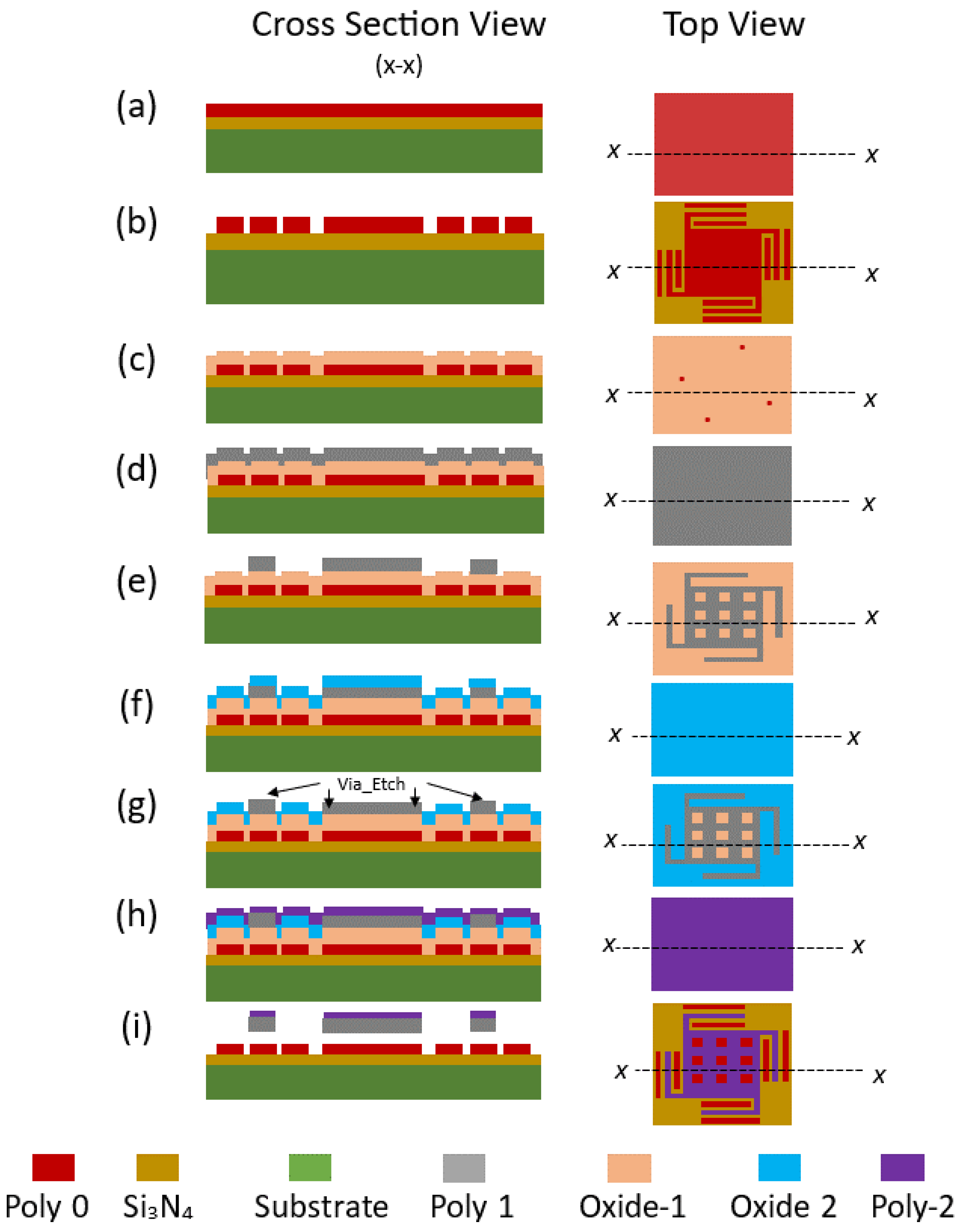
The device was manufactured using PolyMUMPs technology [17]. In this process, polysilicon layers serve as the structural elements, while oxide layers act as sacrificial layers to create cavities and separation between the top plate and the bottom electrode. The process initiates with 100 mm n-type (100) silicon wafers. Next, a 600 nm silicon nitride layer is deposited onto the substrate using low-pressure chemical vapor deposition (LPCVD). Silicon nitride serves as an excellent electrical insulator and a barrier layer against impurity diffusion into the substrate. Following this, a 500 nm layer of polysilicon, known as Poly-0, is deposited onto the nitride layer (Figure 5a). The Poly-0 layer is subsequently photolithographically patterned and etched via a reactive ion etching (RIE) process to produce the fixed bottom electrodes of the MEMS varactor (Figure 5b). A 2 µm phosphosilicate glass (PSG) sacrificial layer, referred to as Oxide-1, is then deposited via LPCVD onto the wafer surface (Figure 5c) and annealed at 1050 °C for 1 h in argon. Oxide-1 is then patterned and RIE-etched to form the anchors of the structure (Figure 5c). The first structural layer, Poly-1, is deposited onto the oxide layer with a thickness of 2.0 µm (Figure 5d), followed by a thin (200 nm) layer of PSG to act as a hard mask. An annealing process at 1050 °C for 1 h dopes the polysilicon with phosphorus from both the PSG layers above and below it while reducing net stress in the Poly-1 layer. The polysilicon and its PSG masking layer are lithographically patterned using a mask designed for the first structural layer, Poly-1 (Figure 5e). The PSG layer is etched to create a hard mask for subsequent polysilicon etching. After etching the polysilicon, the photoresist is removed, and the remaining oxide hard mask is eliminated using RIE. Another sacrificial layer, a second oxide layer, is typically deposited onto the wafer surface and annealed (Figure 5f). This second oxide is patterned using the Poly1_Poly2_VIA level mask, which creates etch holes down to the Poly-1 layer, providing a mechanical and electrical connection between the Poly-1 and Poly-2 layers. Then, the oxide is RIE-etched (Figure 5g). The second structural layer, Poly-2, is then deposited with a thickness of 1.5 μm (Figure 5h), followed by the deposition of 200 nm PSG. As with Poly-1, the thin PSG layer acts as both an etch mask and a dopant source for Poly-2. An annealing step at 1050 °C for one hour dopes the polysilicon and reduces residual film stress in the Poly-2 layer. The Poly-2 layer is lithographically patterned using the POLY-2 mask, and the PSG and polysilicon layers are etched using the same processing conditions as for Poly-1. The photoresist is then removed, and the masking oxide is stripped. In the areas where Poly1_Poly2_VIA patterns are present, the Poly-1 and Poly-2 layers are bonded together to create the membrane structure in our designs. Furthermore, the wafer is patterned lithographically with the final mask, and a 0.5 µm metal layer is deposited and patterned using a liftoff process. This metal layer is solely used for the connection pads. The last step involves releasing the structure (Figure 5i) by etching the sacrificial oxide layer in hydrofluoric acid (HF). The chips are then rinsed with deionized (DI) water, followed by alcohol and critical point drying to avoid stiction.
Figure 6 represents the overall layout of the designed MEMS varactor. Poly-0 serves as the routing layer, facilitating the connection between the capacitor plates and the contact pad. A 0.5 µm layer of gold was deposited and precisely patterned using the liftoff technique, exclusively dedicated to creating the metal connections for the pads.
A scanning electron microscope (SEM) photograph of the fabricated MEMS variable capacitor is presented in Figure 7a. The figure includes all the dimensions of the designed MEMS varactor. An optimization procedure was implemented to enhance the performance of the variable capacitor, aiming for a higher resonance frequency while preserving its compact size. This procedure involved optimizing the dimensions of the electrodes, the suspensions beams, and the membrane. This optimization was crucial to prevent any initial contact between the two parallel plates before applying a voltage, all while ensuring that it did not compromise the out-of-plane electrostatic repulsive force. To facilitate the rapid and complete release of sacrificial layers, release holes were added into the membrane structure. Given that we utilized the PolyMUMPs fabrication process for this design, several parameters were constrained by the inherent limitations of the process. This includes factors such as the initial gap distance, the minimum allowable gap between electrodes, and the minimum width of the electrodes, the thickness of the membranes. The dimensions of the springs in the design were meticulously optimized using finite element analysis (FEA) software, specifically COMSOL Multiphysics 5.3. This methodology enabled us to strike a balance between optimizing the design area and preserving the operational efficiency of the variable capacitor. Figure 7b represents a closeup SEM photograph to show different poly films used in the fabrication process. Due to the substantial difference in dimensions between the anchored beam and the membrane, it is evident that the resistance of the anchored beam significantly outweighs that of the membrane. Since the leg structure consists of two stacked layers of poly, we can approximate the calculation as two parallel resistances. According to the electrical characteristics of the PolyMUMPs process layers, the typical resistance for the Poly-1 film is 10 Ω/sq, while the Poly-2 film registers 20 Ω/sq. Table 1 summarizes the equivalent resistances of the structure.
3. Characterization and Results
The experimental setup used in this study is depicted in Figure 8. The unaligned fixed electrodes were electrically grounded, whereas the bottom aligned fixed electrode and the moving membrane were electrically connected to a DC voltage source. The moving membrane was coupled to an AC voltage source via a bias-T. This increases the airgap; therefore, the capacitance between the moving membrane and the aligned fixed electrode change. The capacitance between the top and bottom aligned electrodes was measured using a B&K precision model 889B LCR meter while sweeping the DC voltage across a range of values (0–100 V), with each measurement recorded. The resulting data were analyzed to evaluate the impact of repulsive actuation on the linearity of the parallel-plate MEMS varactors.
The measured C–V response of the fabricated MEMS variable capacitor using the LCR meter is presented in Figure 9. The linearity factor (LF) was calculated based on:
where Vi and Ci are the voltage and capacitance at the ith data point, respectively, and n is the total data points [10]. The LF value represents close the curve is to a straight line. Thus, the LF value is 100% when a curve is a perfect straight line. The LF of the measured C–V response is 99.7% throughout the usage span (0–100 V), representing a capacitance range of 110–8.48 fF.
Table 2 compares the proposed design to state-of-the-art varactors. The MEMS varactor design proposed here is unique because it has no pull-in voltage restrictions. The displacement of the membrane and moving electrodes occurs out-of-plane in the +z direction away from the aligned fixed electrode, making it distinct from conventional closing-gap MEMS varactor designs. This feature expands the potential applications of the varactor, as it can be operated over a wider voltage, and hence the capacitance range. Figure 10 illustrates the simulated trend of the displacement of the capacitor plate with the applied voltage.
4. Conclusions
The new MEMS varactor design based on a repulsive actuation mechanism introduced in this paper exhibits an ultra-linear capacitance–voltage response. Prototypes were fabricated using the commercial MEMS technology PolyMUMPs from MEMSCAP, and measurements show a linearity factor of 99.7% in the C–V response over a control voltage range from 0 V to 100 V, corresponding to a capacitance range of 110 fF to 8.48 fF, without any risk of encountering a pull-in limitation. This development has significant potential in enabling high-performance MEMS-based tunable devices for various applications, e.g., VCOs and PLL circuits.
Author Contributions
Conceptualization, R.B.; methodology, R.B. and H.H.T.; validation, R.B. and M.Y.E.; investigation, R.B.; resources, M.Y.E. and M.N.E.-G.; writing—original draft preparation, R.B.; writing—review and editing, R.B., M.Y.E., H.H.T. and M.N.E.-G.; supervision, M.N.E.-G.; funding acquisition, F.N. All authors have read and agreed to the published version of the manuscript.
Funding
This research was partially funded by École de technologie supérieure: 212046.
Data Availability Statement
The data that support the findings of this study are available from the corresponding author upon reasonable request.
Acknowledgments
The authors would like to acknowledge the support and assistance provided by the Canadian Microelectronics Corporation (CMC) in fabricating the MEMS devices discussed in this paper.
Conflicts of Interest
The authors declare no conflict of interest.
References
- Lázaro, A.; Girbau, D.; Pradell, L. Distortion produced by RF MEMS varactors on digital communication signals. Microw. Opt. Technol. Lett. 2006, 48, 246–249. [Google Scholar] [CrossRef]
- Quintero, A.; Cardes, F.; Perez, C.; Buffa, C.; Wiesbauer, A.; Hernandez, L. A VCO-based CMOS readout circuit for capacitive MEMS microphones. Sensors 2019, 19, 4126. [Google Scholar] [CrossRef] [PubMed]
- Salvia, J.C.; Melamud, R.; Chandorkar, S.A.; Lord, S.F.; Kenny, T.W. Real-time temperature compensation of mems oscillators using an integrated micro-oven and a phase-locked loop. J. Microelectromechanical Syst. 2010, 19, 192–201. [Google Scholar] [CrossRef]
- Khan, F.; Younis, M.I. RF MEMS electrostatically actuated tunable capacitors and their applications: A review. J. Micromechanics Microengineering 2022, 32, 19. [Google Scholar] [CrossRef]
- Rebeiz, G.M.; Dussopt, L. RF MEMS: Theory, Design, and Technology; John Wiley & Sons: Hoboken, NJ, USA, 2003. [Google Scholar]
- Shaheen, S.; Saleem, M.M.; Zaidi, S.M.T. Design and FEM Modeling of an Electrostatic RFMEMS Varactor. In Proceedings of the International Conference on Computing, Electronic and Electrical Engineering, Quetta, Pakistan, 12–13 November 2018. [Google Scholar]
- Elshurafa, A.; Ho, P.; Salama, K.N. Low voltage RF MEMS variable capacitor with linear C-V response. Electron. Lett. 2012, 48, 392–393. [Google Scholar] [CrossRef]
- Chen, K.; Kovacs, A.; Peroulis, D. Anti-biased RF MEMS varactor topology for 20–25 dB linearity enhancement. In Proceedings of the 2010 IEEE MTT-S International Microwave Symposium, Anaheim, CA, USA, 23–28 May 2010. [Google Scholar]
- Roy, A.L.; Bhattacharya, A.; Chaudhuri, R.R.; Bhattacharyya, T.K. Analysis of the Pull-In Phenomenon in Microelectromechanical Varactors. In Proceedings of the 25th International Conference on VLSI Design, Hyderabad, India, 7–11 January 2012. [Google Scholar]
- Chang-Hoon, H.; Dong-Hoon, C.; Jun-Bo, Y. Parallel-Plate MEMS Variable Capacitor With Superior Linearity and Large Tuning Ratio Using a Levering Structure. J. Microelectromechanical Syst. 2011, 20, 1345–1354. [Google Scholar]
- Chang-Hoon, H.; Dong-Hoon, C.; Seon-Jin, C. MEMS variable capacitor with superior linearity and large tuning ratio by moving the plate to the increasing-gap direction. In Proceedings of the IEEE 24th International Conference on Micro Electro Mechanical Systems, Cancun, Mexico, 23–27 January 2011. [Google Scholar]
- Barrière, F.; Passerieux, D.; Mardivirin, D.; Pothier, A.; Blondy, P. An inverted-gap analog tuning RF-MEMS capacitor with 250 milliwatts power handling capability. In Proceedings of the International Conference on Micro Electro Mechanical Systems (MEMS), Paris, France, 29 January 2012–2 February 2012. [Google Scholar]
- Shavezipur, M.; Khajepour, A.; Hashemi, S.M. Development of novel segmented-plate linearly tunable MEMS capacitors. J. Micromechanics Microengineering 2008, 18, 035035. [Google Scholar] [CrossRef]
- Aryal, N.; Emadi, A. A Method to Enhance Stroke Level of a MEMS Micromirror with Repulsive Electrostatic Force. Micromachines 2020, 11, 401. [Google Scholar] [PubMed]
- He, S.; Mrad, R.B. Design, Modeling, and Demonstration of a MEMS Repulsive-Force Out-of-Plane Electrostatic Micro Actuator. J. Microelectromechanical Syst. 2008, 17, 532–547. [Google Scholar]
- Weimin, W.; Qiang, W.; Hao, R.; Wenying, M.; Chuankai, Q.; Zexiang, C.; Bin, F. Electrostatic repulsive out-of-plane actuator using conductive substrate. Sci. Rep. 2016, 6, 35118. [Google Scholar]
- Cowen, A.; Hardy, B.; Mahadevan, R.; Wilcenski, S. PolyMUMPs Design Handbook; MEMSCAP: Bernin, France, 2011. [Google Scholar]
Figure 1.
Conceptual schematics for (a) a conventional attractive-based MEMS variable capacitor device and (b) newly proposed device with repulsive actuation mechanism resulting in a highly linear C–V response.
Figure 1.
Conceptual schematics for (a) a conventional attractive-based MEMS variable capacitor device and (b) newly proposed device with repulsive actuation mechanism resulting in a highly linear C–V response.
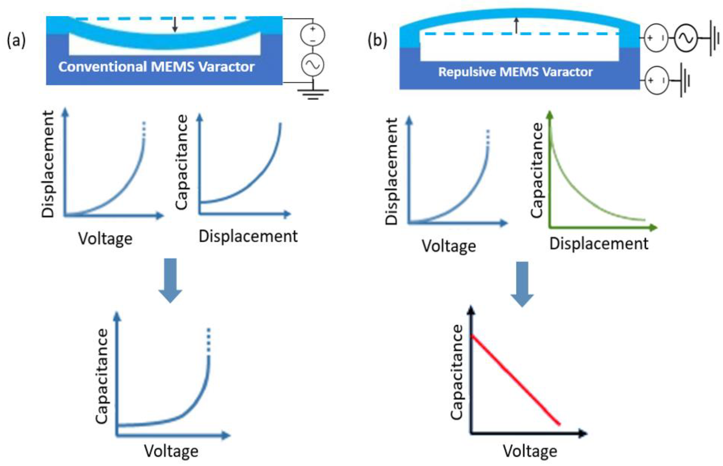
Figure 2.
(a) Schematic view of the movable electrode and the three bottom electrodes. (b) The distribution of the generated electrostatic force, resulting in an upward movement. Blue represents lower displacement values, while red indicates higher displacements.
Figure 2.
(a) Schematic view of the movable electrode and the three bottom electrodes. (b) The distribution of the generated electrostatic force, resulting in an upward movement. Blue represents lower displacement values, while red indicates higher displacements.

Figure 3.
Equivalent capacitances per unit cell.

Figure 4.
Simplified RLC model for the proposed MEMS varactor.
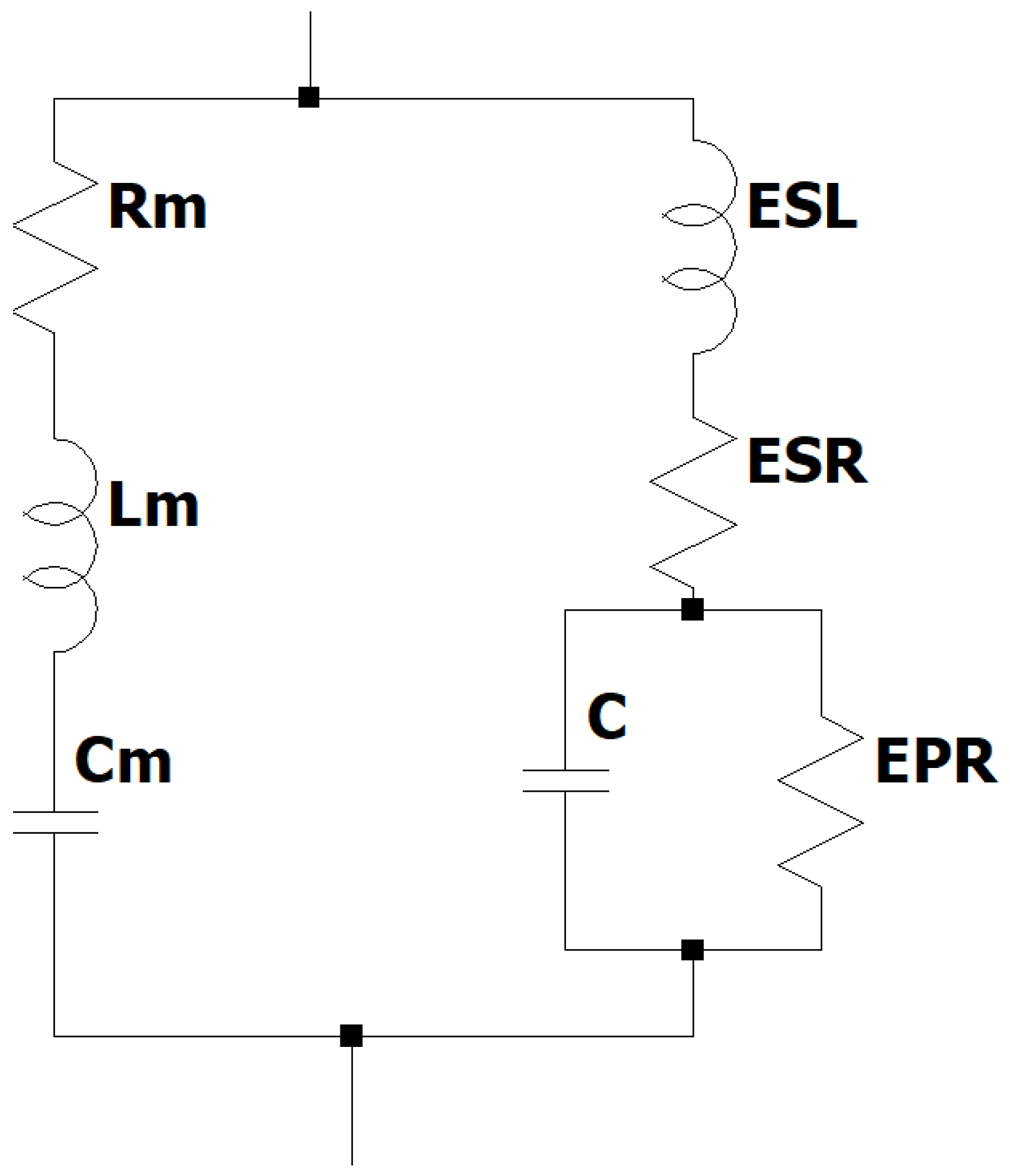
Figure 5.
Top and cross-sectional views, illustrating the fabrication process flow of the proposed MEMS varactor using PolyMUMPs.
Figure 5.
Top and cross-sectional views, illustrating the fabrication process flow of the proposed MEMS varactor using PolyMUMPs.

Figure 6.
Final layout of the proposed MEMS varactor design.
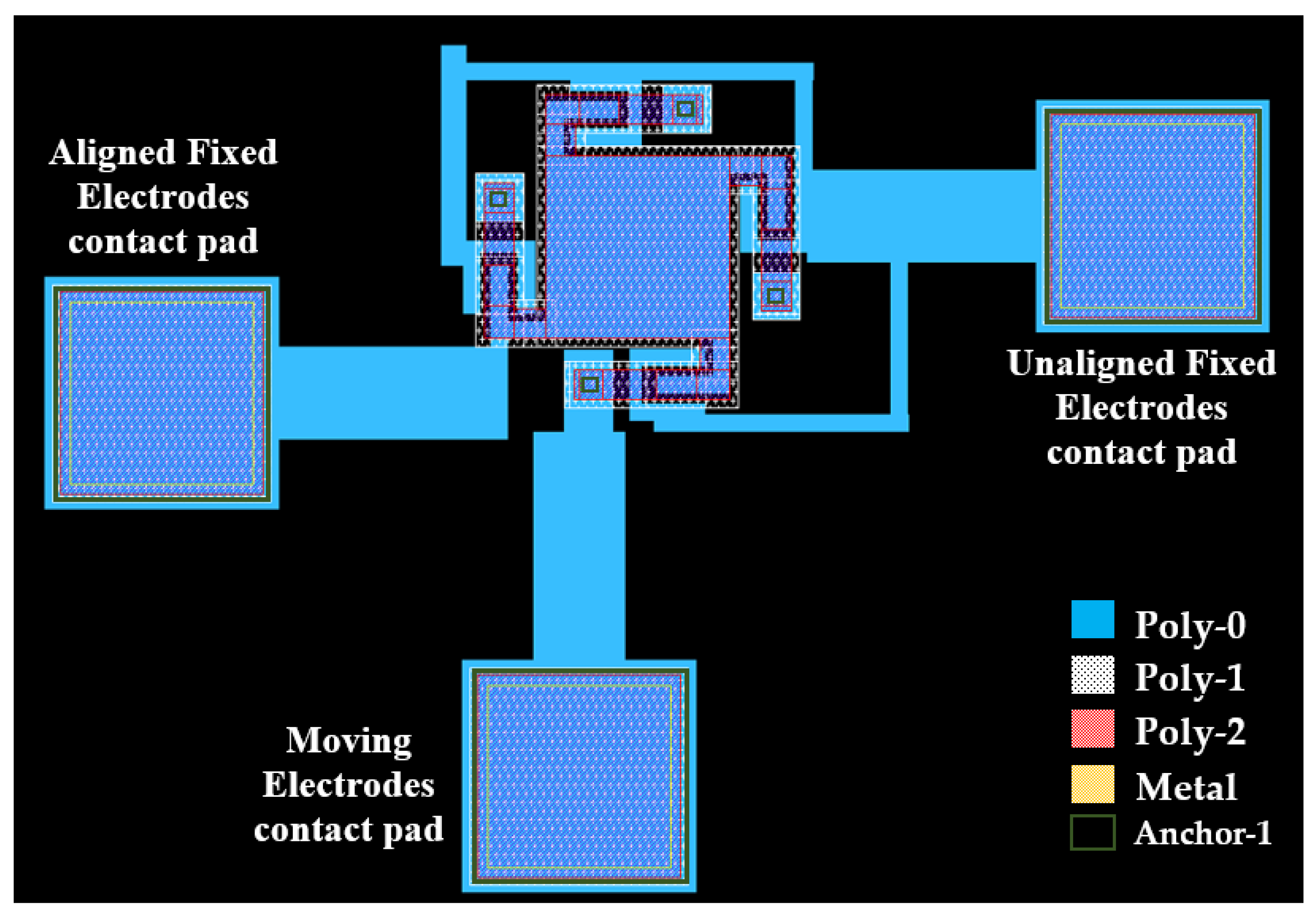
Figure 7.
(a) SEM of the proposed MEMS varactor; (b) SEM image highlighting diverse Poly-Si films employed during fabrication.
Figure 7.
(a) SEM of the proposed MEMS varactor; (b) SEM image highlighting diverse Poly-Si films employed during fabrication.

Figure 8.
Schematic of the experimental setup used to characterize the MEMS varactor.
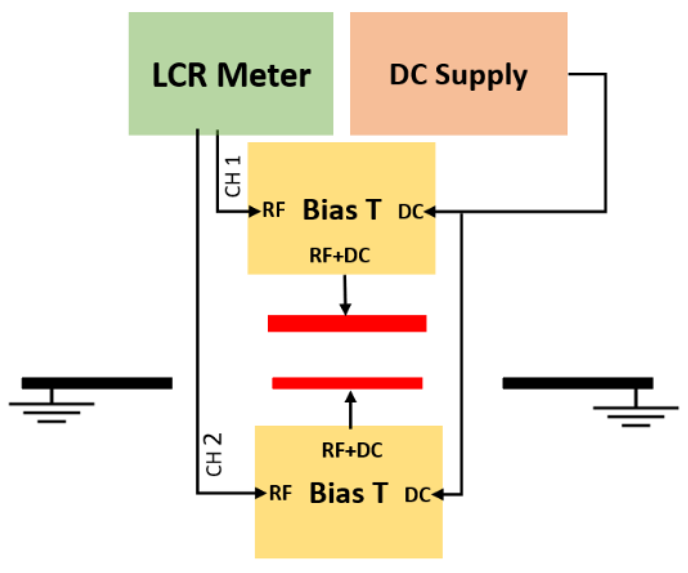
Figure 9.
Measured results of the capacitance of the proposed MEMS varactor vs. the applied voltage.
Figure 9.
Measured results of the capacitance of the proposed MEMS varactor vs. the applied voltage.

Figure 10.
Simulated trend of the displacement of the capacitor plate with the applied voltage.


Table 1.
Comparison with existing MEMS varactors from the literature.
| Structure | Length (μm) | Width (μm) | Resistance (Ω) |
|---|---|---|---|
| Membrane | 100 | 100 | 6.67 |
| Anchored Beam | 85 | 16 | 35.42 |
| Beam to Membrane Interconnect | 17.5 | 16 | 7.29 |
Table 2.
Comparison with existing MEMS varactors from the literature.
| Reference | Linearity Factor | Pull-in Limitations | Varactor Area (mm²) | Min Measured Capacitance | Max Measured Capacitance | Tuning Range Factor | Membrane Movement Direction |
|---|---|---|---|---|---|---|---|
| [6] | 96.07% | Yes | 2.25 | 0.45 pF | 1.125 pF | 1.6 | +Z |
| [7] | 98.50% | Yes | 0.068 | 0.75 pF | 0.9 pF | 0.2 | −Z |
| [10] | 98.40% | Yes | 0.16 | 0.42 pF | 1.05 pF | 1.34 | +Z |
| [11] | 99.10% | Yes | 0.16 | 0.5 pF | 1.3 pF | 1.78 | +Z |
| [12] | 96.20% | Yes | − | 60 fF | 235 fF | 2.92 | +Z |
| [13] | 99.00% | Yes | 0.16 | 0.51 pF | 0.8 pF | 0.57 | −Z |
| This Work | 99.70% | No | 0.031 | 8.5 fF | 110 fF | 11.94 | +Z |
Disclaimer/Publisher’s Note: The statements, opinions and data contained in all publications are solely those of the individual author(s) and contributor(s) and not of MDPI and/or the editor(s). MDPI and/or the editor(s) disclaim responsibility for any injury to people or property resulting from any ideas, methods, instructions or products referred to in the content. |
© 2023 by the authors. Licensee MDPI, Basel, Switzerland. This article is an open access article distributed under the terms and conditions of the Creative Commons Attribution (CC BY) license (https://creativecommons.org/licenses/by/4.0/).
Share and Cite
MDPI and ACS Style
Bensalem, R.; Elsayed, M.Y.; Tawfik, H.H.; Nabki, F.; El-Gamal, M.N. Enhancing Linearity in Parallel-Plate MEMS Varactors through Repulsive Actuation. Micro 2023, 3, 811-821. https://doi.org/10.3390/micro3040057
AMA Style
Bensalem R, Elsayed MY, Tawfik HH, Nabki F, El-Gamal MN. Enhancing Linearity in Parallel-Plate MEMS Varactors through Repulsive Actuation. Micro. 2023; 3(4):811-821. https://doi.org/10.3390/micro3040057
Chicago/Turabian StyleBensalem, Roufaida, Mohannad Y. Elsayed, Hani H. Tawfik, Frederic Nabki, and Mourad N. El-Gamal. 2023. "Enhancing Linearity in Parallel-Plate MEMS Varactors through Repulsive Actuation" Micro 3, no. 4: 811-821. https://doi.org/10.3390/micro3040057