
Real-Time Compact Digital Processing Chain for the Detection and Sorting of Neural Spikes from Implanted Microelectrode Arrays

Department of Information Engineering, Electronics and Telecommunications-DIET, University of Rome “La Sapienza”, 00184 Rome, Italy
*
Author to whom correspondence should be addressed.
Chips 2024, 3(1), 32-48; https://doi.org/10.3390/chips3010002
Submission received: 21 November 2023
/
Revised: 30 January 2024
/
Accepted: 6 February 2024
/
Published: 8 February 2024
(This article belongs to the Topic Applied System on Biomedical Engineering, Healthcare and Sustainability 2023)
Abstract
:Implantable microelectrodes arrays are used to record electrical signals from surrounding neurons and have led to incredible improvements in modern neuroscience research. Digital signals resulting from conditioning and the analog-to-digital conversion of neural spikes captured by microelectrodes arrays have to be elaborated in a dedicated DSP core devoted to a real-time spike-sorting process for the classification phase based on the source neurons from which they were emitted. On-chip spike-sorting is also essential to achieve enough data reduction to allow for wireless transmission within the power constraints imposed on implantable devices. The design of such integrated circuits must meet stringent constraints related to ultra-low power density and the minimum silicon area, as well as several application requirements. The aim of this work is to present real-time hardware architecture able to perform all the spike-sorting tasks on chip while satisfying the aforementioned stringent requirements related to this type of application. The proposed solution has been coded in VHDL language and simulated in the Cadence Xcelium tool to verify the functional behavior of the digital processing chain. Then, a synthesis and place and route flow has been carried out to implement the proposed architecture in both a 130 nm and a FD-SOI 28 nm CMOS process, with a 200 MHz clock frequency target. Post-layout simulations in the Cadence Xcelium tool confirmed the proper operation up to a 200 MHz clock frequency. The area occupation and power consumption of the proposed detection and clustering module are 0.2659 mm2/ch, 7.16 μW/ch, 0.0168 mm2/ch, and 0.47 μW/ch for the 130 nm and 28 nm implementation, respectively.
1. Introduction
In the last decade, there has been a growing interest in the development of implanted neural interfaces for monitoring brain activity with very high temporal and spatial resolution. Implantable microelectrodes arrays, implemented in microelectromechanical system (MEMS) technology, are used to record electrical signals from surrounding neurons and have led to outstanding and innovative results in recent neuroscience research. These electrodes are able to detect action potentials (APs) from individual neurons, which are very important not only for studying individual neurons but networks of neurons in order to understand how the activity of interconnected neurons results in higher-order functions such as perception, understanding, movement, and memory [1,2,3].
In neural microsystems, neural signals, captured from MEMS microelectrodes, are passed to the analog front-end chain, which is devoted to signal conditioning, and whose first stage is a front-end amplifier, followed by an additional filter/amplification stage that drives an analog-to-digital (ADC) converter. The overall bandwidth of the neural recording interfaces typically ranges from 0.1 Hz up to 10 kHz. The high-frequency content (about 200 Hz to 5000 Hz) is referred to as single unit action potentials (AP), while the low-frequency signal content (below about 200 Hz) is referred to as local field potentials (LFP) [4].
This processing chain is replicated many times to achieve a multichannel acquisition system, which is essential for monitoring several neurons belonging to different brain regions. The information acquired through such neural microsystems can be used for the prevention and treatment of many neurological diseases (such as epilepsy or Parkinson’s) and in the so-called brain–machine–interfaces (BMI) [5,6]. Therefore, the system is composed of a network of MEMS sensors which are devoted to the acquisition of neural signals, known as “action potentials” or “spikes”, for the realization of implantable multi-electrodes arrays (MEA). Then, the acquired very weak neural signals, with amplitudes in the order of 10 µV to 100 µV, are amplified and filtered before the A/D conversion process takes place because different cellular mechanisms are responsible for different frequency components of the recorded signals, as mentioned above. This chain is usually replicated several times in order to obtain a multi-channel system able to monitor wide brain regions and collect information from a high number of neurons. Communications between neurons happen through the aforementioned spike signals. Each microelectrode captures neural activity from multiple surrounding neurons. These extracellular recordings are called multi-unit activities because they involve spikes from different source neurons and are useful only in specific cases. However, several applications, ranging from clinical diagnostic and medical technology to BMI, which are used to control external devices such as neural robotic prosthesis and so on, require single-unit activity, that is, classification of spikes based on source neurons from which they were emitted. The process of classifying spikes with the corresponding source neurons, namely, the process of separating multi-unit activity into groups of single-unit activity, is called “spike sorting”, and it consists of three main phases: “Detection and Alignment”, “Features Extraction”, and “Clustering” [7,8,9,10,11,12].
Reducing the output sorting data rate while minimizing the latency between spike detection and spike classification is the primary objective of real-time spike-sorting solutions. This is due to the fact that stimulating neurons during certain temporal windows is necessary to cause synaptic change. Different types of synaptic modifications are produced, for instance, by stimulation that occurs 20 ms before or after pre-synaptic activation [7]. Therefore, in closed-loop BMI applications, the sorting latency is a critical consideration.
Hardware design solutions to implement the different algorithms for each task of the spike-sorting chain are currently being investigated in order to obtain optimal performance for the entire neural spike-sorting system. Several techniques and digital architectures, able to achieve a reduction of hardware resources, have been presented in the literature in order to process a higher and higher number of neurons with minimal hardware resources and power consumption [7,8,9,10,11,12]. Indeed, integrated circuits of such complexity have to satisfy stringent requirements related to power density since it has been demonstrated that the power density has to be less than 277 μW/mm2 to be safe because high power values generate heat that damages the surrounding brain tissue [13]. Another important requirement is to avoid circuits with heat flux over 40 mW/mm2, which may damage the brain tissue [14]. Finally, the minimization of the silicon area is very important for implantable devices devoted to the processing of signals coming from a larger and larger number of neurons.
Moreover, real-time processing of neural data is essential to control neural robotic applications and for several experiments which cannot be performed otherwise. Sorted results are preferably wirelessly transmitted to avoid issues such as risk of injury and infection as well as the degradation of the signal quality. For instance, among the previous spike-sorting digital signal processing (DSP) cores proposed in the literature, a single-channel real-time spike-sorting chip with a silicon area of 2.57 mm2 and a power consumption of 2.78 μW from a 1.16 V power supply has been presented in [7]. A 16-channel spike-sorting chip, which occupies 0.07 mm2 of area per channel (i.e., a total of 1.23 mm2) with a power consumption of 4.68 μW per channel (i.e., a total of 75 μW) from a 0.27 V supply voltage implemented in a 65-nm CMOS process, has been reported in [12].
From the perspective of the design of integrated circuits dedicated to these applications, the miniaturization of these systems presents many challenges. Indeed, modern neural recording microsystems involve different trade-offs between the area and power consumption constraints on one side, and performance requirements in terms of accuracy, speed, and latency of the sorting operations on the other side.
The aim of this work is to develop the processing chain of a CMOS-integrated circuit for implantable neural spike-sorting systems, able to operate with ultra-low power consumption as well as with minimum silicon area footprint. The focus is oriented on a fixed-point digital architecture for the detection and clustering phases in which the tradeoff between performance parameters (such as accuracy, maximum number of clusters, and maximum number of waveforms to be stored) and silicon area and power consumption constraints has to be optimized.
The paper is organized as follows. Section 2 summarizes the background of spike-sorting systems and discusses the selection of the algorithms which have been implemented. Section 3 provides simulation and synthesis results both for detection and clustering block, which allow us to identify the digital architecture to be implemented. In Section 4, the digital architecture and its hardware implementation on two different CMOS processes is described, and finally, Section 5 is devoted to the conclusion.
2. Background and Algorithms Selection
The main blocks of a typical spike-sorting signal processing chain are shown in Figure 1, where the different phases are highlighted. The digitized neural signals, available at the output of the ADC block, are sent through the “Detection and Alignment” module, where spikes are extracted from background noise and aligned to a common temporal reference point relative to the spike waveform.
These aligned spikes are sent to the “feature extraction” module, where the latter are processed to extract a set of features of the spike shape to allow for a better separation of the different spike classes. At this point, some sort of dimensionality reduction process takes place, whose target is the identification of feature coefficients that best separate spikes. More specifically, starting from all the samples used to represent the spike waveform, the most discriminative features are extracted, thus reducing the dimensionality of the neural waveform and allowing for a simpler discrimination process between the different spikes. Finally, based on the extracted features coefficients, spikes are mapped into different groups associated to the different neurons; this process is known as “clustering”. The result of the whole process is the train of spike times for each neuron, namely, the desired single-unit activity.
Accurate selection of the most suitable state-of-the-art algorithms for each of the main tasks in the spike-sorting process is crucial. Indeed, algorithms directly affect hardware resources, and consequently, different trade-offs are involved, principally in terms of silicon area and power consumption, bearing in mind that another essential factor lies in the accuracy of the results that can be achieved with a given type of algorithm, which, among other things, has to be unsupervised and real-time. Moreover, neuronal activity produces a dynamic environment; thus, in order to identify clusters of arbitrary shape and size, adaptability is another important characteristic. Therefore, complexity/accuracy of algorithms must be taken into account in order to find the optimal trade-off.
2.1. Detection Strategies
The detection phase is very critical, and since it is the first step in the processing of the neural spikes, it has to be performed with high accuracy. Indeed, the aim of this task is to discriminate the neural spike signals from the background noise. Moreover, since neuronal activity produces a dynamic environment, the detection algorithms have to be able to overcome non-ideality issues, such as non-Gaussian noise, non-stationarities, and overlapping spikes.
- Absolute value.
- Non-linear energy operators (NEOs):
- ○
- Conventional NEO;
- ○
- KNEO;
- ○
- Smoothed NEO (SNEO).
The absolute value technique performs better than applying a simple thresholding technique, but it is still weak in handling different SNR scenarios and other non-idealities such as non-Gaussian noise. The non-linear energy operators are very attractive techniques with which to process the neural data coming from the ADC in order to emphasize the high-frequency and high-energy content (related to neural spikes) and to attenuate the low-frequency and low-energy content (related to noise). Indeed, the first refers to the presence of a spike signal which is characterized by a rapid variation in the time domain of the waveform, which is a high-frequency event in the frequency domain. Moreover, the energy of the spike is higher than the energy of the noise; therefore, these techniques are very helpful for detection purposes. In this context, by defining , the output of the conventional NEO method applied on the current sample , the following formulation can be defined [17]:
The threshold can be computed as a simple average on the NEO waveform, weighted by a constant to be found empirically from the processing of different datasets [16].
The KNEO method is very similar to the conventional NEO, except for the k parameter used as shift factor; indeed, in the standard NEO, , but in the general case, any value of k can be chosen. The formulation is very straightforward, and with the same convention used before, the output of the KNEO processing can be defined as [16]
where k can be any integer value (coherent with the application). The thresholding method is the same as the NEO.
The SNEO is based on the application of a smoothing window to the neural data processed with the KNEO method. In particular, once the KNEO is performed, a convolution of the entire sequence with a suitable filter window is performed. The approach can be defined as [16]
where represents the output of the KNEO process, and is a given filtering window selected with a proper length and type (for instance, a Hamming window of length 25 samples). The thresholding technique is selected to be the same as the other NEO variants, and it is reported in the following equation [16]:
In this work, the focus is on the non-linear energy operator algorithm and its variants because of their simple hardware implementation (which is suitable for applications with stringent area and power consumption requirements) and their ability to guarantee good detection accuracy. This point will be better assessed in the next section, where the three NEO variants will be compared both in terms of detection accuracy and hardware resources.
2.2. Features Extraction Approaches
The step of feature extraction within the spike-sorting system is used in order to select, among all the samples collected to represent the spike waveform, the more discriminative ones, which are used to obtain a sort of dimensionality reduction of the data, to be used in the following clustering phase. The main features extraction approaches adopted in the literature are [18] as follows:
- Principal component analysis (PCA);
- Wavelet transform (WLT);
- Discrete derivatives (DD);
- Samples windowing (SW).
In the PCA technique, the signal samples are processed in order to build the orthogonal basis (i.e., the principal components (PC)), which are used to address the directions in the data with the largest variation. This orthogonal bases are calculated through the eigenvalue decomposition of the covariance matrix of the data and then each spike is represented with coefficients [18].
The wavelet transform approach is used to decompose the signal into shifted and scaled version of a so called “wavelet”; this method, unlike the Fourier analysis, which uses decomposition of the signal through a sine wave, is able to detect abrupt changes in the signal which cannot be appreciated with sinusoidal decomposition. Indeed, a wavelet, unlike a sine wave, is a rapidly decaying wave-like oscillation. There are different types of “mother wavelet”, each with different shapes in order to select the one that best fits the particular changes in the signals under analysis [18].
The DD method is based on the computation of the slope at each sample point with different time scales:
where is the time shift used for the processing and can be an integer, like the following:
The samples windowing approach simply involves the selection of a window of samples of the signal waveform around the peak identified with the NEO operator. This last technique can be successfully applied when adopting the OSort clustering algorithm, as in [7], and provides the advantage that the average of each cluster is itself a spike waveform representing the whole cluster.
2.3. Clustering
Clustering, in the general meaning of the word, is related to the identification of common characteristics of the data within a particular set and it is very widely used in the field of data science to analyze very large datasets. In particular, different data are evaluated in order to separate them into the corresponding membership groups. In the field of neural spike sorting, only some subsets of this type of algorithm are used to separate the multi-unit activity into single-unit activities. These single units are a better approximation of neuronal activity than unclustered data. The spike analysis is heavily dependent on the clustering phase which allows us to obtain the separation of groups of neurons based on the spatiotemporal behavior of the single spike signal. One of the most discriminative characteristics of choosing one clustering algorithm rather than another one is the possibility to perform it in a real-time environment. Indeed, not all the clustering algorithms can be used in real-time (unsupervised) applications, since some of them require the knowledge of some information before the scenario can be analyzed and processed. The latter are called offline or supervised, and in the context of neural spike-sorting systems, dedicated to real-time processing they cannot be used. Clearly, another key factor is the classification accuracy that can be reached with a given type of algorithm, and in this respect, the offline algorithms are most attractive.
Clustering algorithms are categorized based on the nature of their working mechanism, such as partitional, hierarchical, probabilistic, graph-theory, fuzzy logic, density-based, and learning-based. For a complete comprehension of each of the latter, the reader can refer to [19,20,21,22,23,24,25,26,27,28,29,30,31,32,33].
In order to choose the most suitable algorithm for our hardware implementation, we analyzed the literature with a particular focus on algorithms suitable to be implemented in real time. The results of this literature survey are reported in Table 1, where a comparison of the key parameters involved in the selection phase of the clustering algorithm is provided. Data summarized in Table 1 have been extracted mainly from [18,24,25,29,30].
The OSort algorithm was chosen for our implementation because it is able to work in real time and its hardware implementation is much simpler than the other machine learning implementations that have been recently presented.
Osort is a very attractive approach since its working mechanism is very intuitive and simple. It is a clustering algorithm used in real-time application which uses an iterative process based on a comparison of “distances” between the extracted features or the time domain, windowed, spike waveforms. In fact, it can work properly with or without an explicit feature extraction process; indeed, it can also be used directly to process a window of samples of the dataset (SW feature extraction approach).
The algorithm flow graph is shown in Figure 2. The incoming spike waveform is used as input, and the Euclidean distance is calculated between the incoming spike waveform with samples s(n) and the mean waveform of the existing clusters with samples c(n):
where represents the number of samples in the spike window. The parameter “d” is calculated for all the available existing clusters (clearly, if no clusters have been generated yet, the spike is assigned to the first generated one, and it coincides also with the mean value of the cluster since no other spikes are present within the cluster). If more clusters are present, different Euclidean distances will be calculated, and the minimum ones are used to be compared with a given threshold parameter , extracted as the variance of the noise of the dataset.
When a given spike is assigned to a given cluster, the mean value of the latter will be updated with the information contained in the new spike, and the updating of the mean value is performed according to the following equation:
where N defines the number of spikes present in the particular cluster. When this process is terminated, a further check is performed in which the distance “k” between the generated clusters is also computed in order to verify if some clusters can be merged together. If, again, the minimum one is less than the same threshold, then the clusters can be merged; otherwise, the algorithm starts again with the first step through an iteration process that ends only when all the spikes have been processed.
3. Simulation Framework and Processing Chain Definition
3.1. Simulation Datasets
The datasets used for simulation purposes have been obtained from the University of Leicester website [34], where simulated datasets that have been widely used in the evaluation of spike-sorting algorithms are available. These synthetic datasets have been generated by adding spike waveform templates to background noise of various levels, and the different datasets have been generated using different spike templates. Examples of waveforms from three different datasets and two different noise standard deviations are reported in Figure 3.
3.2. Automatic Threshold Selection
In our simulation framework, a way to handle the selection of the optimal threshold to be used for online processing is adopted. This is also very useful in evaluating the different detection approaches with respect to a realistic environment in order to know where and when a detection failure occurs. The proposed approach, for the first part of the implementation, is similar to the one presented in [15], and in choosing the optimal detection threshold, it consists of different steps:
- Perform different iterations by varying the threshold from 0 to max (ψ[x(n)]) and plot a graph for the number of detected spikes;
- Calculate and plot the gradient of the number of detected spikes;
- At the point where the number of detected spikes will stop changing drastically, there will be a drop in the gradient curve;
- Find the peak in the gradient graph.
It has to be noted, however, that as stated in [15], the peak of the gradient does not always correspond to the optimal point for the threshold selection, and this is due to the fact that the detection process has to cope with different SNR scenarios and other non-idealities. Therefore, starting from this peak, the optimal point should be sought in the next few points of the gradient curve. In this context, we propose a way to select the optimal point. Indeed, denoting the true times of the spike events which are available from the synthetic datasets with , and defining the times of the simulated spike events (which are the actual times for which the framework has detected a spike) with , their difference can be used as a metric to be minimized. More specifically, the optimal threshold can be defined as the one for which the above metric is minimized:
Indeed, both and are 1-D arrays whose number of elements is the same as the number of samples of the detected spikes. By performing the difference between them, another array containing the corresponding difference can be obtained. This array is computed for each threshold used, and the index is used to identify the threshold value selected (extracted from the gradient curve) in the framework. The index corresponding to the minimum distance between the spike times is the one related to the optimal threshold. The result of this process can be observed in Figure 4, where the optimal threshold value is found after four iterations, and with this value, the real and actual spikes times are almost overlapped.
3.3. Detection: Simulation and Synthesis Results on the Different NEO Operators
In this subsection, the simulation results achieved with the different spike detection algorithms based on the NEO and its variants are described. In particular, the comparisons are based on the accuracy results obtained with the three techniques discussed in Section 2.1. The accuracy formulation can be obtained by using the definition of the probability of detection () and the probability of false alarm ():
where TP, FP, and FN are the true positive, the false positive, and the false negative, respectively. In this way, is possible to define the accuracy metric as
In Table 2, Table 3, Table 4 and Table 5, the different accuracy results for the available datasets are reported. The numbers in the name of the dataset (such as, for example, 01 in the dataset Noise_01) are related to the noise standard deviation and therefore to the SNR of the waveform; the higher the number, the lower the SNR. Normalized noise level ranging from 0.05 to 0.2 are equivalent to a signal-to-noise ratio (SNR) range decreasing from about 16 to about 3 [18,34]. The above tables show that the best results can be achieved with the SNEO approach over a wide range of SNR values and different dataset scenarios; although, as expected, the performance degrades at low SNR for all the simulated methods, the SNEO technique can achieve better results with respect to the other NEO variants. These improvements can be related to the filtering process involved in the SNEO by exploiting a smoothing window on the neural data.
The configurations used for the different techniques are the ones that can lead to the best achievable accuracy for a certain technique. Therefore, different combinations of “K” and “C” parameters are used, and in statistical terms, the “best” values are found for
and
Finally, the corresponding hardware resources needed to implement the different detection techniques are reported in Table 6 after synthesis via the field-programmable gate array (FPGA), 130 nm, and 28 nm CMOS processes. Both the FPGA and application-specific integrated circuit (ASIC) hardware resources estimations show that all the tested techniques are very prone to be implemented into synthesizable digital hardware architectures, although the SNEO variant requires the highest area since it involves the additional step of the smoothing window process.
The analysis of simulated accuracy and resources usage reported above suggests that the simple NEO allows us to achieve the best trade-off between accuracy and hardware resources usage, and it has been chosen for our hardware implementation.
3.4. Features Extraction and Clustering: Simulation Results on the OSort Clustering with DD and SW Features
We also exploited the simulation framework to compare two different features extraction approaches; the DD and the SW techniques were applied to the OSort clustering algorithm. More complex approaches, such as PCA and WLT, have not been considered because the main aim of this work was to develop an ultra-compact processing chain.
In Table 7, the clustering accuracy is calculated for different datasets (first column), considering as input both the features generated through the DD approach (second column) and the waveforms samples windowed through the SW technique (third column). The accuracy is calculated taking into account how many spikes are present in each cluster compared with the true number of spikes obtained from the simulator datasets. The accuracy results in Table 7 show that the increase in the level of noise leads to a drop in the accuracy of the sorting, as expected. Another outcome from these simulations is that the value of in the DD approach has to be changed across the different datasets to achieve good results (Table 7 reports accuracy data for the best choice of for each dataset), whereas the accuracy using the SW approach is more reliable. For this last reason, we have chosen the SW strategy for the hardware implementation. Another important advantage of using the waveforms samples for clustering purposes is that in this way, the average of each cluster in the OSort algorithm corresponds to a cluster-representative spike waveform.
4. Implementation of Real-Time Detection and Sorting Chain
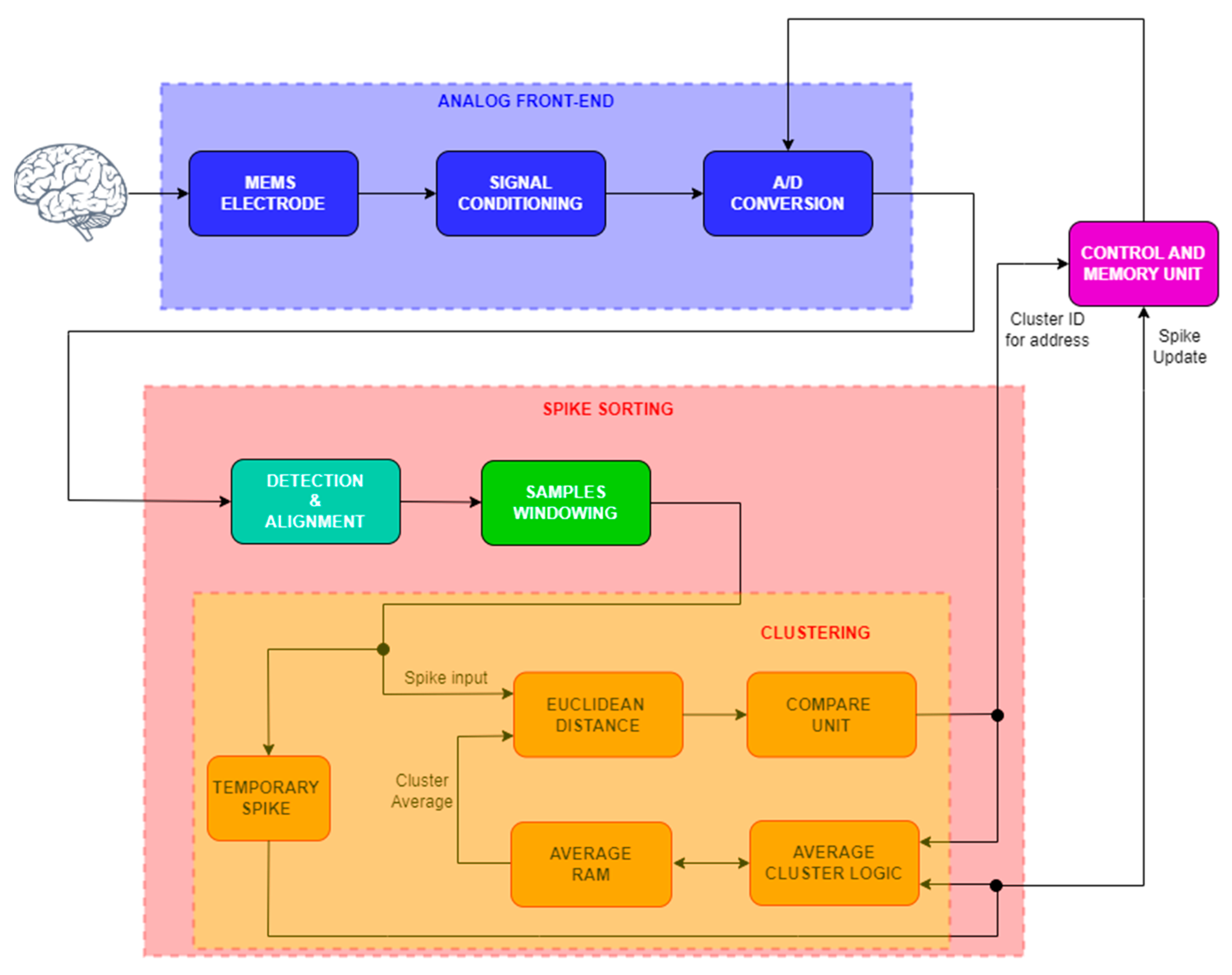
The proposed architecture for the neural spike detection and sorting channel is reported in Figure 5. The signal conditioning block within the analog front-end is used for amplification and filtering of the neural signals taken from the MEMS microelectrode array, which are then converted into the proper binary format by the ADC block for subsequent digital processing. The digitized neural spikes are passed to the digital processing chain for detection and alignment operations and are then sent to the spike-sorting unit through a windowing module. The data flow from the ADC to the digital blocks is managed by the control and memory unit block. More specifically, the control and memory unit has in charge the generation of the signals controlling the ADC conversion, the optional storing of all the incoming waveforms (if needed), and the management of detection and sorting operations within the digital processing chain.
The operations of NEO detection, alignment, and samples windowing are performed in the first part of the digital processing chain. NEO is chosen because it involves less hardware resources and enough accuracy of detection compared to other NEO variants which are similar in terms of accuracy but require a little bit more resources. To minimize the area footprint, a window of 32 samples of the detected and aligned spikes is sent to the OSort unit, as explained in Section 3.
This architecture has been designed in order to enable the simultaneous processing of several channels, which has now become mandatory for future neural recording applications [31,33].
It has to be noted that when operating in real-time, the OSort algorithm should continue to accept incoming identified spikes in order to compute fresh cluster averages and perform cluster merger checks. Using a queue to hold all recently discovered spikes is one way to solve the problem, but doing so would need a significant amount of silicon area. As an alternative, we propose to compare incoming spikes to the pre-existing clusters while simultaneously performing cluster merging and averaging.
The proposed digital clustering channel is made up of the following blocks:
- Euclidean distance;
- Compare unit;
- Average logic computation;
- Average memory to store the average waveform of a given cluster.
The “Euclidean distance” block is used to compute the Euclidean distance, already described in (8); it is designed as a simple accumulator which accumulates the results between the squared distance among the samples of the spike and the samples of the actual spike average, which is representative of the cluster mean waveform and stores it in the average memory. This operation is replicated a number of times equal to the number of clusters present in the memory. The proposed architecture is thought to handle a maximum of eight clusters. This distance is passed to the “Compare unit” block, which contains several flip-flops (FFs) used as registers to store the minimum distance among all the computed distances (one for each cluster); a comparison between the next distance and the actual stored is performed, and if the new distance is less than the actual one, then it will be stored into the FFs, overwriting the past data.
The “Compare unit” then sends to its output the cluster ID (a simple number from 0 to 7) for which the distance is the minimum one. The ID is used to perform the write operation in the proper cluster address into the “Average memory” unit, which takes as input the new average computed between the old average and the actual spike, present at the input of the digital core sorter and maintained in a temporary file register for all the time needed to complete the operations. At the end of the process, the classified spikes can be stored into the proper cluster address region related to the cluster ID computed by the compare unit. The merging step of the OSort algorithm is performed as in [7].
The main design parameters assumed for the implementation of the proposed spike-sorting module are as follows:
- Data Size: 8 bits.
- Memory for average waveforms: 256 locations (8 clusters with 32 samples per spike window) of 8 bits of data.
- Accumulator size: 24 bits.
The choice of a data size of only 8 bits is due to the main aim of this work, which is an aggressive reduction of the area footprint of the spike-sorting module. For this purpose, it has to be noted that the effective number of bits (ENOB) of most ADCs for neural recording applications is typically limited to 8–9 bits [34].
Due to its limited size, and to allow for fully parallel access to all locations, the “Average memory” module has been implemented with conventional D flip-flops from the standard-cell library.
The synthesis and place and route of the proposed digital processing chain have been performed using the Cadence Genus Synthesis Solution and the Cadence Innovus tool, respectively. The spike sampling frequency is 24 kHz, and each detected spike is saved as a 32 samples window, namely, a window of 1.3 ms duration.
The digital verification of the whole architecture was carried out by developing a dedicated SystemVerilog test for each designed block and performing a simulation in the Cadence Xcelium tool. Then, the whole architecture was verified with a bit true test between the RTL and the Simulink architecture developed through SystemVerilog direct programming interface (DPI) generation, which is an interface between SystemVerilog and programming languages such as C. The HDL verifier can generate SystemVerilog DPI components from MATLAB code or Simulink models for use in ASIC verification [35]. Finally, post-layout simulations (PLS) were performed.
The implementation has been carried out in two different technologies: a well-established bulk 130 nm CMOS technology; and a recently developed 28 nm fully depleted silicon on insulator (FDSOI) CMOS process. A summary of area requirements is reported in Table 8, in which the results of the synthesis have been reported for detection with the SW feature extraction module (second column) and for the clustering block (third column).
The area estimation is very low; indeed, only about 0.00862 mm2 is reported for the single channel, and a clock frequency of about 200 MHz can be reached.
Detection and clustering blocks have then been placed and routed in the Cadence environment using the Innovus tool and referring to both the 130 nm and 28 nm technologies. The layout of the single channel digital processing chain implemented within the Cadence Innovus place and route tool in the 28 nm technology is reported in Figure 6, showing an area footprint as low as 125 μm × 125 μm.
Since the proposed implementation can be operated with a clock frequency as high as 200 MHz, which is about 8333 times the typical sampling frequency of neural recording systems, the proposed clustering unit can be time shared between several neural recording channels. In this case, the main design constraint would be the memory to store all the neural spikes coming from the different channels. For example, to save a maximum of 16 waveforms made up of 32 8-bit samples for a maximum of eight clusters, 32 kbits of memory for each channel are needed. If an 8192-channel sorting is considered, the clock frequency has to be set at 196.6 MHz, which is compatible with the proposed design, but the memory requirement to store all the spike waveforms would be 256 Mbits, which is clearly not compatible with conventional on-chip integration.
To save this huge amount of memory, two possible strategies can be devised. The first approach, which we have considered in our work, is to store on chip only the average waveforms of the spikes, with the associated cluster IDs and spike times providing the address of the clustered spikes to an optional external memory. Another approach, which could be explored in future research, would be to consider time-division-multiplexed systems, such as the high-density CMOS neural probes [36,37,38,39,40], which allow for the recording of a large number of neurons at single-cell resolution. For example, referring to the system in [38], the ADC directly converts 1024-time-division-multiplexed channels with a sampling frequency in the range of 24.6 MHz, allowing for the exploitation of the high clock frequency achieved by the proposed spike-sorting module in a simpler manner.
A comparison against the state of the art is reported in Table 9, showing how the proposed digital processing chain implemented in the 28 nm technology achieves the lowest silicon area footprint and power consumption per channel.
The closest competitor with the proposed spike-sorting module is the implementation in [31] based on the binary decision tree (DT) clustering approach. Considering a technology scaling from a 130 nm process to a 28 nm process, the DT spike-sorting module would outperform the proposed one in terms of area and power consumption per channel. It has to be noted, however, that the area and power consumption estimations provided in [31] are based on post-synthesis results.
5. Conclusions
In the first part of this work, a comparison and an evaluation of the most used detection algorithms is performed, and in particular, the focus is oriented towards the energy operator type, which are very prone to be used in this field of application since they require very low hardware resources. Indeed, their simple hardware implementation and its capacity to achieve high accuracy results are very attractive in the context of neural spike detection applications. Based on the information acquired during the simulation phase, the SNEO technique seems to be the best candidate for the detection step and can be used in future design of CMOS integrated circuits for an implantable neural spike-sorting system framework. However, in this work, the simple NEO algorithm is chosen since the difference in terms of accuracy results does not justify the extra use of area resources.
Then, two features extraction approaches applied to the OSort algorithm have been considered in the simulation phase. Since the OSort clustering technique using the SW features has demonstrated a good accuracy with the most commonly adopted datasets, and since its implementation is the simplest one, it has been chosen for the implementation of the digital processing chain developed in this work.
The implementation results have demonstrated an area occupation and power consumption of the proposed detection and clustering module of 0.2659 mm2/ch, 7.16 μW/ch, 0.0168 mm2/ch, and 0.47 μW/ch for the 130 nm and 28 nm implementation, respectively. The comparison against the state of the art has shown how the proposed spike-sorting module achieves the lowest silicon area footprint and power consumption per channel. In fact, even if the proposed architecture moves some functions in the control and memory unit to simplify the implementation of the clustering module, this results in a strongly reduced area and power consumption when several digital channels have to be elaborated. The achieved low area occupation is also related to the adopted data size of only 8 bits, which, even if lower than the one adopted in other works, is acceptable for neural recording applications due to the limited ENOB (in the range of 8–9 bits) of ADCs used in such systems.
The proposed spike-sorting module could be exploited in time-division-multiplexed systems, which, in the near future, will rely on ADCs able to convert 8192-time-division-multiplexed channels directly with a sampling frequency in the range of 196.6 MHz and will allow us to exploit, fully, the 200 MHz clock frequency achieved by this implementation.
Author Contributions
Conceptualization, A.V. and G.S.; methodology, G.S.; software, A.V. and R.C.; validation, A.V., R.C. and G.S.; formal analysis, A.V.; investigation, A.V.; resources, A.V.; writing—original draft preparation, A.V.; writing—review and editing, G.S.; supervision, G.S.; project administration, G.S. All authors have read and agreed to the published version of the manuscript.
Funding
This research received no external funding.
Institutional Review Board Statement
Not applicable.
Informed Consent Statement
Not applicable.
Data Availability Statement
Data are contained within the article.
Conflicts of Interest
The authors declare no conflicts of interest.
References
- Steinmetz, N.A.; Koch, C.; Harris, K.D.; Carandini, M. Challenges and opportunities for large-scale electrophysiology with Neuropixels probes. Curr. Opin. Neurobiol. 2018, 50, 92–100. [Google Scholar] [CrossRef]
- Hong, G.; Lieber, C.M. Novel electrode technologies for neural recordings. Nat. Rev. Neurosci. 2019, 20, 330–345. [Google Scholar] [CrossRef] [PubMed]
- Urai, A.E.; Doiron, B.; Leifer, A.M.; Churchland, A.K. Large-scale neural recordings call for new insights to link brain and behavior. Nat. Neurosci. 2022, 25, 11–19. [Google Scholar] [CrossRef] [PubMed]
- Reich, S.; Sporer, M.; Ortmanns, M. A chopped neural front-end featuring input impedance boosting with suppressed offset-induced charge transfer. IEEE Trans. Biomed. Circuits Syst. 2021, 15, 402–411. [Google Scholar] [CrossRef]
- Lebedev, M.; Nicolelis, A. Brain-Machine Interfaces: Past, present and future. Trends Neurosci. 2006, 29, 536–546. [Google Scholar] [CrossRef] [PubMed]
- Harrison, R.R. The design of integrated circuits to observe brain activity. Proc. IEEE 2008, 96, 1203–1216. [Google Scholar] [CrossRef]
- Valencia, D.; Alimohammad, A. Real-time spike sorting system using parallel OSort clustering. IEEE Trans. Biomed. Circuits Syst. 2019, 13, 1700–1713. [Google Scholar] [CrossRef] [PubMed]
- Olsson, R., III; Wise, K. A three dimensional neural recording microsystem with implantable data compression circuitry. IEEE J. Solid-State Circuits 2005, 40, 2796–2804. [Google Scholar] [CrossRef]
- Chae, M.; Yang, Z.; Yuce, M.R.; Hoang, L.; Liu, W. A 128-channel 6mW wireless neural recording IC with spike feature extraction and UWB transmitter. IEEE Trans. Neural Syst. Rehabil. Eng. 2009, 17, 312–321. [Google Scholar] [CrossRef]
- Karkare, V.; Gibson, S.; Marković, D. A 130 µW, 64-channel, spike-sorting DSP chip. IEEE J. Solid State Circuits 2011, 46, 1214–1222. [Google Scholar] [CrossRef]
- Liu, Y.; Sheng, J.; Herbordt, M.C. A Hardware Design for In-Brain Neural Spike Sorting. In Proceedings of the 2016 IEEE High Performance Extreme Computing Conference (HPEC), Waltham, MA, USA, 13–15 September 2016. [Google Scholar]
- Karkare, V.; Gibson, S.; Marković, D. A 75 µW, 16-channel, Neural Spike-Sorting Processor With Unsupervised Clustering. IEEE J. Solid-State Circuits 2013, 48, 2230–2238. [Google Scholar] [CrossRef]
- Kim, S.; Tathireddy, P.; Normann, R.A.; Solzbacher, F. Thermal impact of an active 3-D microelectrode array implanted in the brain. IEEE Trans. Neural Syst. Rehabil. Eng. 2007, 15, 493–501. [Google Scholar] [CrossRef]
- Wolf, P.D. Thermal considerations for the design of an implanted cortical brain–machine interface (BMI). In Indwelling Neural Implants: Strategies for Contending with the In Vivo Environment; Reichert, W.M., Ed.; CRC Press: Boca Raton, FL, USA, 2008. [Google Scholar]
- Malik, M.H.; Saeed, M.; Kamboh, A.M. Automatic Threshold Optimization in Nonlinear Energy Operator Based Spike Detection. In Proceedings of the IEEE Engineering in Medicine and Biology Society (EMBC), Conference Paper, Orlando, FL, USA, 16–20 August 2016. [Google Scholar]
- Saggese, G.; Tambaro, M.; Vallicelli, E.A.; Strollo, A.G.M.; Vassanelli, S.; Baschirotto, A.; De Matteis, M. Comparison of Sneo-Based Neural Spike Detection Algorithms for Implantable Multi-Transistor Array Biosensors. Electronics 2021, 10, 410. [Google Scholar] [CrossRef]
- Gibson, S.; Judy, J.W.; Markovic, D. Technology-Aware Algorithm Design for Neural Spike Detection, Feature Extraction, and Dimensionality Reduction. IEEE Trans. Neural Syst. Rehabil. Eng. 2010, 18, 469–478. [Google Scholar] [CrossRef] [PubMed]
- Kalantari, F.; Hosseini-Nejad, H.; Sodagar, A.M. Hardware-Efficient, On-the-Fly, On-Implant Spike Sorter Dedicated to Brain-Implantable Microsystems. IEEE Trans. Very Large Scale Integr. Syst. 2022, 30, 1098–1106. [Google Scholar] [CrossRef]
- Jin, X.; Han, J. Partitional Clustering. In Encyclopedia of Machine Learning; Sammut, C., Webb, G.I., Eds.; Springer: Boston, MA, USA, 2011. [Google Scholar]
- Patel, S.; Sihmar, S.; Jatain, A. A study of hierarchical clustering algorithms. In Proceedings of the 2015 2nd International Conference on Computing for Sustainable Global Development (INDIACom), New Delhi, India, 11–13 March 2015; pp. 537–541. [Google Scholar]
- Jain, A.K.; Dubes, R.C. Algorithms for Clustering Data; Prentice Hall: Upper Saddle River, NJ, USA, 1988. [Google Scholar]
- Zhao, Y.; Karypi, G. Hierarchical Clustering Algorithms for Document Datasets. Data Min. Knowl. Discov. 2005, 10, 141–168. [Google Scholar] [CrossRef]
- Veerabhadrappa, R.; Ul Hassan, M.; Zhang, J.; Bhatti. A Compatibility Evaluation of Clustering Algorithms for Contemporary Extracellular Neural Spike Sorting. Front. Syst. Neurosci. 2020, 14, 34. [Google Scholar] [CrossRef] [PubMed]
- Saeed, M.; Khan, A.A.; Kamboh, A.M. Comparison of Classifier Architectures for Online Neural Spike Sorting. IEEE Trans. Neural Syst. Rehabil. Eng. 2017, 25, 334–344. [Google Scholar] [CrossRef] [PubMed]
- Sinaga, K.P.; Yang, M.-S. Unsupervised K-Means Clustering Algorithm. IEEE Access 2020, 8, 80716–80727. [Google Scholar] [CrossRef]
- Saeed, M.; Kamboh, A.M. Hardware architecture for on-chip unsupervised online neural spike sorting. In Proceedings of the 2013 6th International IEEE/EMBS Conference on Neural Engineering (NER), San Diego, CA, USA, 6–8 November 2013; pp. 1319–1322. [Google Scholar]
- Paraskevopoulou, S.E.; Wu, D.; Eftekhar, A.; Constandinou, T.G. Hierarchical Adaptive Means (HAM) clustering for hardware-efficient, unsupervised and real-time spike sorting. J. Neurosci. Methods 2014, 235, 145–156. [Google Scholar] [CrossRef]
- Gibson, S. Neural Spike Sorting in Hardware: From Theory to Practice. Ph.D. Thesis, University of California Los Angeles, Los Angeles, CA, USA, 2012. [Google Scholar]
- Daniel, V.; Alimohammad, A. Neural spike sorting using binarized neural networks. IEEE Trans. Neural Syst. Rehabil. Eng. 2020, 29, 206–214. [Google Scholar]
- Schäffer, L.; Nagy, Z.; Kincses, Z.; Fiáth, R.; Ulbert, I. Spatial Information Based OSort for Real-Time Spike Sorting Using FPGA. IEEE Trans. Biomed. Eng. 2021, 68, 99–108. [Google Scholar] [CrossRef] [PubMed]
- Yang, Y.; Boling, S.; Mason, A.J. A hardware-efficient scalable spike sorting neural signal processor module for implantable high-channelcount brain machine interfaces. IEEE Trans. Biomed. Circuits Syst. 2017, 11, 743–754. [Google Scholar] [CrossRef] [PubMed]
- Zamani, M.; Jiang, D.; Demosthenous, A. An adaptive neural spike processor with embedded active learning for improved unsupervised sorting accuracy. IEEE Trans. Biomed. Circuits Syst. 2018, 12, 665–676. [Google Scholar] [CrossRef]
- Liu, Y.; Luan, S.; Williams, I.; Rapeaux, A.; Constandinou, T.G. A 64-Channel Versatile Neural Recording SoC With Activity-Dependent Data Throughput. IEEE Trans. Biomed. Circuits Syst. 2017, 11, 1344–1355. [Google Scholar] [CrossRef]
- Quian, Q.R. Simulated Dataset; University of Leicester: Leicester, UK, 2020. [Google Scholar] [CrossRef]
- Available online: https://it.mathworks.com/discovery/asic-verification.html (accessed on 7 February 2024).
- Steinmetz, N.A.; Aydin, C.; Lebedeva, A.; Okun, M.; Pachitariu, M.; Bauza, M.; Beau, M.; Bhagat, J.; Böhm, C.; Broux, M.; et al. Neuropixels 2.0: A miniaturized high-density probe for stable, long-term brain recordings. Science 2021, 372, eabf4588. [Google Scholar] [CrossRef] [PubMed]
- Angotzi, G.N.; Boi, F.; Lecomte, A.; Miele, E.; Malerba, M.; Zucca, S.; Casile, A.; Berdondini, L. SiNAPS: An implantable active pixel sensor CMOS-probe for simultaneous large-scale neural recordings. Biosens. Bioelectron. 2019, 126, 355–364. [Google Scholar] [CrossRef]
- Boi, F.; Locarno, A.; Ribeiro, J.F.; Tonini, R.; Angotzi, G.N.; Berdondini, L. Coupling SiNAPS High-density Neural Recording CMOS-Probes with Optogenetic Light Stimulation. In Proceedings of the 2021 IEEE Biomedical Circuits and Systems Conference (BioCAS), Berlin, Germany, 7–9 October 2021. [Google Scholar]
- Trautmann, E.M.; Hesse, J.K.; Stine, G.M.; Xia, R.; Zhu, S.; O’Shea, D.J.; Karsh, B.; Colonell, J.; Lanfranchi, F.F.; Vyas, S.; et al. Large-scale High-density brain-wide neural recording in nonhuman primates. bioRxiv, 2023. [Google Scholar] [CrossRef]
- Paulk, A.C.; Kfir, Y.; Khanna, A.R.; Mustroph, M.L.; Trautmann, E.M.; Soper, D.J.; Stavisky, S.D.; Welkenhuysen, M.; Dutta, B.; Shenoy, K.V.; et al. Large-scale neural recordings with single neuron resolution using Neuropixels probes in human cortex. Nat. Neurosci. 2022, 25, 252–263. [Google Scholar] [CrossRef]
Figure 1.
Block scheme of the signal processing chain for spike sorting.

Figure 2.
OSort algorithm flow graph.

Figure 3.
Examples of waveforms from three different datasets with noise standard deviation of 0.05 (a) and noise standard deviation of 0.2 (b).
Figure 3.
Examples of waveforms from three different datasets with noise standard deviation of 0.05 (a) and noise standard deviation of 0.2 (b).

Figure 4.
Real and actual spike times for the optimal threshold value at iteration 3 (a) and at iteration 4 (b).
Figure 4.
Real and actual spike times for the optimal threshold value at iteration 3 (a) and at iteration 4 (b).

Figure 5.
Proposed spike-sorting architecture.

Figure 6.
Layout of the single channel digital processing chain implemented within the Cadence Innovus place and route tool in the 28 nm technology.
Figure 6.
Layout of the single channel digital processing chain implemented within the Cadence Innovus place and route tool in the 28 nm technology.


Table 1.
Comparison of clustering algorithms commonly used in spike-sorting systems.
| Clustering Algorithm | Accuracy | Complexity | Autonomous | Training Phase |
|---|---|---|---|---|
| K-Means [24,25] | High | Medium | No | Yes |
| OSort [24,25,26,27,28,29,30] | Medium | Low | Yes | No |
| Self-organizing maps [24] | High | Medium | Yes | Yes |
| Support Vector Machine [24] | High | High | No | Yes |
| Template Matching [18] | High | Medium | Yes | Yes |
| Binarized Neural Network [29] | High | Medium | Yes | Yes |
Table 2.
Accuracy results for dataset “C_Easy1”.
| Noise_01 | Noise_015 | Noise_02 | Noise_025 | Noise_03 | |
|---|---|---|---|---|---|
| SNEO | 99.72% | 97.95% | 95.22% | 93.57% | 87.94% |
| KNEO | 96.26% | 95.83% | 93.54% | 91.68% | 87.08% |
| NEO | 95.83% | 95.12% | 93.48% | 91.55% | 82.90% |
Table 3.
Accuracy results for dataset “C_Easy2”.
| Noise_005 | Noise_01 | Noise_015 | Noise_02 | |
|---|---|---|---|---|
| SNEO | 96.27% | 97.59% | 97.62% | 96.05% |
| KNEO | 92.50% | 91.05% | 92.54% | 91.84% |
| NEO | 91.57% | 90.01% | 91.04% | 91.00% |
Table 4.
Accuracy results for dataset “C_Difficult1”.
| Noise_005 | Noise_01 | Noise_015 | Noise_02 | |
|---|---|---|---|---|
| SNEO | 96.05% | 96.13% | 96.44% | 96.21% |
| KNEO | 91.12% | 90.65% | 90.25% | 91.74% |
| NEO | 90.81% | 89.97% | 89.83% | 90.99% |
Table 5.
Accuracy results for dataset “C_Difficult2”.
| Noise_005 | Noise_01 | Noise_015 | Noise_02 | |
|---|---|---|---|---|
| SNEO | 96.27% | 97.55% | 95.40% | 95.63% |
| KNEO | 92.50% | 90.01% | 90.63% | 90.87% |
| NEO | 91.57% | 89.65% | 90.01% | 90.61% |
Table 6.
Synthesis results for the different energy operator detection algorithms on Xilinx Artix 7 FPGA, CMOS 130 nm, and 28 nm standard-cells library.
Table 6.
Synthesis results for the different energy operator detection algorithms on Xilinx Artix 7 FPGA, CMOS 130 nm, and 28 nm standard-cells library.
| Xilinx Artix 7 FPGA | ASIC 130 nm @FCK = 200 MHz | ASIC 28 nm @FCK = 200 MHz | |||
|---|---|---|---|---|---|
| LUT | FF | DSP | Area (μm2) | Area (μm2) | |
| SNEO | 321 | 0 | 24 | 114,548 | 7268 |
| KNEO | 52 | 69 | 2 | 26,274 | 1685 |
| NEO | 4 | 32 | 2 | 18,527 | 1167 |
Table 7.
Accuracy results for clustering process with discrete derivatives and samples windowing as features extraction approaches.
Table 7.
Accuracy results for clustering process with discrete derivatives and samples windowing as features extraction approaches.
| Dataset | Clustering Accuracy (%) (Discrete Derivatives) | Clustering Accuracy (%) (Samples Windowing) |
|---|---|---|
| δ: ±3, ±5 | SW: 32 Samples | |
| C_Easy1_noise005 | 94.12 | 93.70 |
| C_Easy1_noise01 | 95.76 | 95.21 |
| C_Easy1_noise015 | 89.96 | 94.24 |
| C_Easy1_noise02 | 75.80 | 83.22 |
| C_Easy1_noise025 | 54.85 | 70.08 |
| C_Easy1_noise03 | 41.40 | 59.17 |
| δ: ±1, ±3, ±7 | SW: 32 Samples | |
| C_Easy2_noise005 | 95.13 | 93.41 |
| C_Easy2_noise01 | 94.98 | 91.84 |
| C_Easy2_noise015 | 86.73 | 82.01 |
| C_Easy2_noise02 | 58.39 | 53.65 |
| δ: ±2, ±4, ±6 | SW: 32 Samples | |
| C_Difficult1_noise005 | 94.73 | 91.80 |
| C_Difficult1_noise01 | 92.75 | 74.06 |
| C_Difficult1_noise015 | 85.12 | 73.09 |
| C_Difficult1_noise02 | 71.56 | 72.28 |
Table 8.
Summary of area occupation of the single channel of the proposed architecture in 130 nm and 28 nm CMOS technology from the synthesis tool.
Table 8.
Summary of area occupation of the single channel of the proposed architecture in 130 nm and 28 nm CMOS technology from the synthesis tool.
| Technology | Detection + SW Area [mm2] | Clustering Area [mm2] |
|---|---|---|
| 130 nm | 0.01853 | 0.13663 |
| 28 nm | 0.00118 | 0.00862 |
Table 9.
Comparison with the state of the art.
| Reference | Process [nm] | Detection | Alignment | Clustering | Voltage [V] | Power/Ch [μW/Ch] | Area/Ch [mm2/Ch] |
|---|---|---|---|---|---|---|---|
| This Work | 130 | NEO | Peak | OSort | 1.2 | 7.16 * | 0.2659 ** |
| This Work | 28 | NEO | Peak | OSort | 0.9 | 0.47 * | 0.0168 ** |
| [12] | 65 | AV | Slope | OSort | 0.27 | 4.68 ** | 0.07 * |
| [31] | 130 | NEO | No need | DT-based | 1.2 | 0.75 ** | 0.023 *** |
| [32] | 180 | Sthr& NEO | Peak | CSort | 1.8 | 148 ** | 2.7 * |
| [18] | 180 | AV | Peak | Correlation | 1.8 | 1.74 * | 0.047 ** |
| [7] | 32 | NEO | Peak | OSort | 1.16 | 2.78 * | 2.57 ** |
* Implemented chip; ** post-layout estimation; *** post-synthesis estimation.
Disclaimer/Publisher’s Note: The statements, opinions and data contained in all publications are solely those of the individual author(s) and contributor(s) and not of MDPI and/or the editor(s). MDPI and/or the editor(s) disclaim responsibility for any injury to people or property resulting from any ideas, methods, instructions or products referred to in the content. |
© 2024 by the authors. Licensee MDPI, Basel, Switzerland. This article is an open access article distributed under the terms and conditions of the Creative Commons Attribution (CC BY) license (https://creativecommons.org/licenses/by/4.0/).
Share and Cite
MDPI and ACS Style
Vittimberga, A.; Corelli, R.; Scotti, G. Real-Time Compact Digital Processing Chain for the Detection and Sorting of Neural Spikes from Implanted Microelectrode Arrays. Chips 2024, 3, 32-48. https://doi.org/10.3390/chips3010002
AMA Style
Vittimberga A, Corelli R, Scotti G. Real-Time Compact Digital Processing Chain for the Detection and Sorting of Neural Spikes from Implanted Microelectrode Arrays. Chips. 2024; 3(1):32-48. https://doi.org/10.3390/chips3010002
Chicago/Turabian StyleVittimberga, Andrea, Riccardo Corelli, and Giuseppe Scotti. 2024. "Real-Time Compact Digital Processing Chain for the Detection and Sorting of Neural Spikes from Implanted Microelectrode Arrays" Chips 3, no. 1: 32-48. https://doi.org/10.3390/chips3010002