
Suppressing the Dielectric Loss in Superconducting Qubits through Useful Geometry Design


Abstract
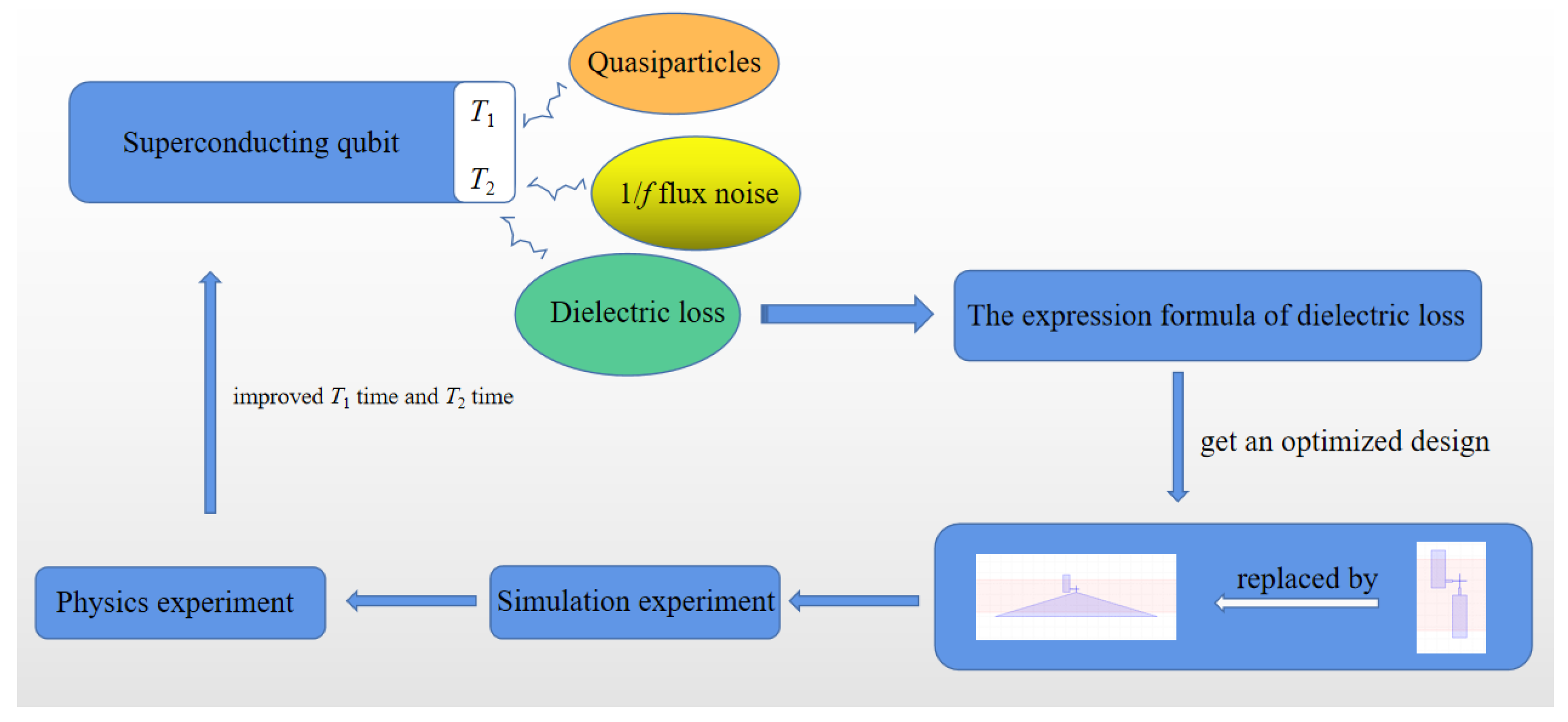
:1. Introduction
2. Methods and Fabrication
2.1. Comparison of Surface Energy between the Straight and Tapered Junction Wires
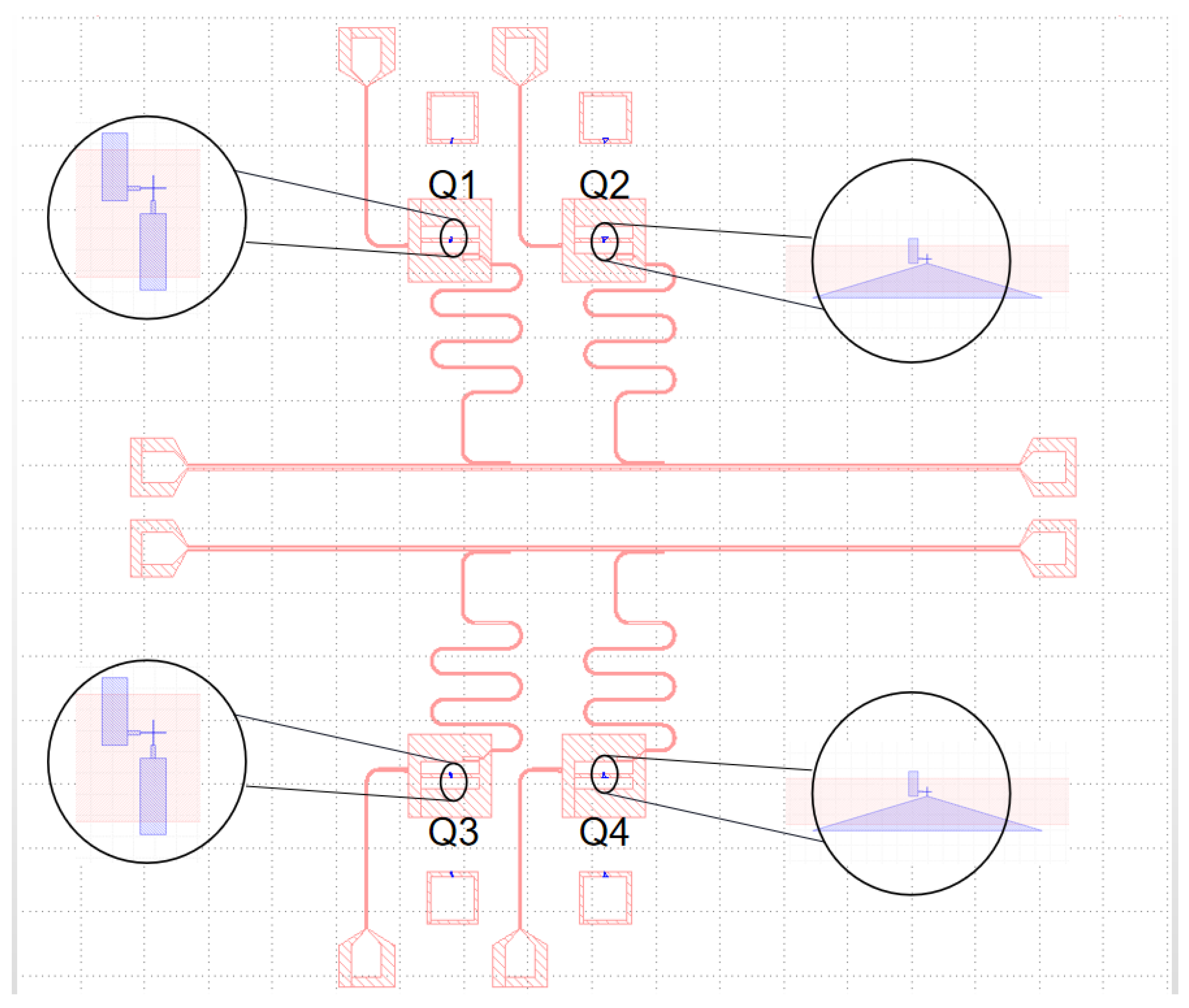
2.2. Design and Fabrication
3. Results
3.1. Simulation Experiment
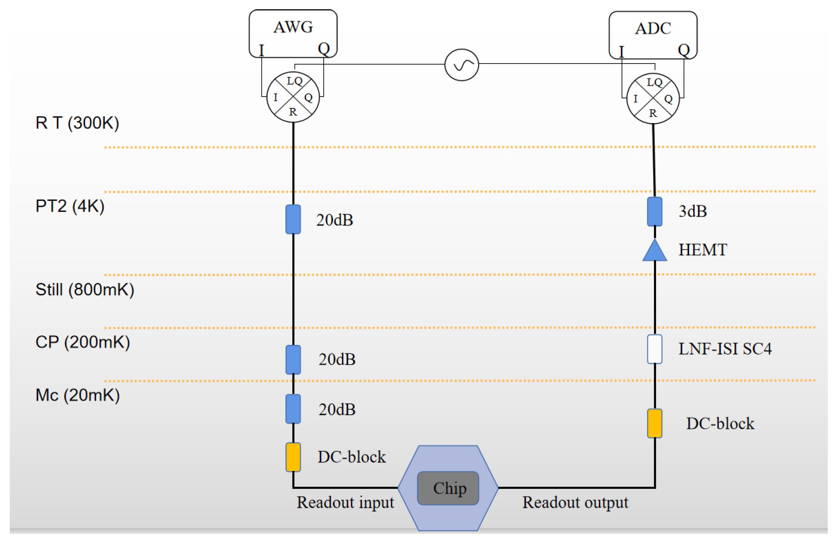
3.2. Physics Experiment
Experimental Setup and Wiring
4. Conclusions
Author Contributions
Funding
Data Availability Statement
Conflicts of Interest
References
- Eagle-Quantum-Processor-Performance. Available online: https://research.ibm.com/blog/eagle-quantum-processor-performance (accessed on 27 May 2022).
- Paik, H.; Schuster, D.I.; Bishop, L.S.; Kirchmair, G.; Catelani, G.; Sears, A.P.; Johnson, B.R.; Reagor, M.J.; Frunzio, L.; Glazman, L.I.; et al. Observation of high coherence in Josephson junction qubits measured in a three-dimensional circuit QED architecture. Phys. Rev. Lett. 2011, 107, 240501. [Google Scholar] [CrossRef] [PubMed] [Green Version]
- Barends, R.; Kelly, J.; Megrant, A.; Sank, D.; Jeffrey, E.; Chen, Y.; Yin, Y.; Chiaro, B.; Mutus, J.; Neill, C.; et al. Coherent josephson qubit suitable for scalable quantum integrated circuits. Phys. Rev. Lett. 2013, 111, 080502. [Google Scholar] [CrossRef] [PubMed]
- Martinis, J.M.; Megrant, A. UCSB final report for the CSQ program: Review of decoherence and materials physics for superconducting qubits. arXiv 2014, arXiv:1410.5793. [Google Scholar]
- Place, A.P.; Rodgers, L.V.; Mundada, P.; Smitham, B.M.; Fitzpatrick, M.; Leng, Z.; Premkumar, A.; Bryon, J.; Vrajitoarea, A.; Sussman, S.; et al. New material platform for superconducting transmon qubits with coherence times exceeding 0.3 milliseconds. Nat. Commun. 2021, 12, 1779. [Google Scholar] [CrossRef] [PubMed]
- Wang, C.; Li, X.; Xu, H.; Li, Z.; Wang, J.; Yang, Z.; Mi, Z.; Liang, X.; Su, T.; Yang, C.; et al. Towards practical quantum computers: Transmon qubit with a lifetime approaching 0.5 milliseconds. NPJ Quantum Inf. 2022, 8, 3. [Google Scholar] [CrossRef]
- Gordon, R.T.; Murray, C.E.; Kurter, C.; Sandberg, M.; Hall, S.A.; Balakrishnan, K.; Shelby, R.; Wacaser, B.; Stabile, A.A.; Sleight, J.W.; et al. Environmental radiation impact on lifetimes and quasiparticle tunneling rates of fixed-frequency transmon qubits. Appl. Phys. Lett. 2022, 120, 074002. [Google Scholar] [CrossRef]
- Gambetta, J.M.; Murray, C.E.; Fung, Y.K.K.; McClure, D.T.; Dial, O.; Shanks, W.; Sleight, J.W.; Steffen, M. Investigating Surface Loss Effects in Superconducting Transmon Qubits. IEEE Trans. Appl. Supercond. 2017, 27, 1700205. [Google Scholar] [CrossRef]
- Dial, O.; McClure, D.T.; Poletto, S.; Keefe, G.A.; Rothwell, M.B.; Gambetta, J.M.; Abraham, D.W.; Chow, J.M.; Steffen, M. Bulk and surface loss in superconducting transmon qubits. Supercond. Sci. Technol. 2016, 29, 044001. [Google Scholar] [CrossRef] [Green Version]
- Murray, C.E. Material matters in superconducting qubits. Mater. Sci. Eng. R Rep. 2021, 146, 100646. [Google Scholar] [CrossRef]
- Woods, W.; Calusine, G.; Melville, A.; Sevi, A.; Golden, E.; Kim, D.K.; Rosenberg, D.; Yoder, J.L.; Oliver, W.D. Oliver Determining Interface Dielectric Losses in Superconducting Coplanar-Waveguide Resonators. Phys. Rev. Appl. 2019, 12, 014012. [Google Scholar] [CrossRef] [Green Version]
- Koch, J.; Terri, M.Y.; Gambetta, J.; Houck, A.A.; Schuster, D.I.; Majer, J.; Blais, A.; Devoret, M.H.; Girvin, S.M.; Schoelkopf, R.J. Charge-insensitive qubit design derived from the Cooper pair box. Phys. Rev. A 2007, 76, 538. [Google Scholar] [CrossRef] [Green Version]
- Deng, H.; Song, Z.; Gao, R.; Xia, T.; Bao, F.; Jiang, X.; Ku, H.S.; Li, Z.; Ma, X.; Qin, J.; et al. Titanium Nitride Film on Sapphire Substrate with Low Dielectric Loss for Superconducting Qubits. arXiv 2022, arXiv:2205.03528. [Google Scholar]
- Wang, C.; Axline, C.; Gao, Y.Y.; Brecht, T.; Chu, Y.; Frunzio, L.; Devoret, M.H.; Schoelkopf, R.J. Surface participation and dielectric loss in superconducting qubits. Appl. Phys. Lett. 2015, 107, 162601. [Google Scholar] [CrossRef] [Green Version]
- Martinis, J.M. Optimal design of a superconducting transmon qubit with tapered wiring. NPJ Quantum 2022, 8, 1–11. [Google Scholar]
- Wenner, J.; Barends, R.; Bialczak, R.C.; Chen, Y.; Kelly, J.; Lucero, E.; Mariantoni, M.; Megrant, A.; O’Malley, P.J.J.; Sank, D.; et al. Surface loss simulations of superconducting coplanar waveguide resonators. Appl. Phys. Lett. 2011, 99, 2012–2015. [Google Scholar] [CrossRef]
- Calusine, G.; Melville, A.; Woods, W.; Das, R.; Stull, C.; Bolkhovsky, V.; Braje, D.; Hover, D.; Kim, D.K.; Miloshi, X.; et al. Analysis and mitigation of interface losses in trenched superconducting coplanar waveguide resonators. Appl. Phys. Lett. 2018, 112, 062601. [Google Scholar] [CrossRef] [Green Version]
- Sandberg, M.; Vissers, M.R.; Kline, J.S.; Weides, M.; Gao, J.; Wisbey, D.S.; Pappas, D.P. Etch induced microwave losses in titanium nitride superconducting resonators. Appl. Phys. Lett. 2012, 100, 262605. [Google Scholar] [CrossRef] [Green Version]
- Potts, A.; Parker, G.J.; Baumberg, J.J.; De Groot, P.A.J. CMOS compatible fabrication methods for submicron Josephson junction qubits. IEE Proc.-Sci. Meas. Technol. 2001, 107, 225–228. [Google Scholar] [CrossRef] [Green Version]
- Costache, M.V.; Bridoux, G.; Neumann, I.; Valenzuela, S.O. Lateral metallic devices made by a multiangle shadow evaporation technique. J. Vac. Sci. 2015, 30, 04E105. [Google Scholar] [CrossRef] [Green Version]


| Qubit | S/T | Fr (GHz) | Fq (GHz) | T1 (μs) | T2 (μs) |
|---|---|---|---|---|---|
| Q1 | S | 6.149 | 5.105 | 12.7 | 0.78 |
| Q2 | T | 6.342 | 5.287 | 16.4 | 3.49 |
| Q3 | S | 6.159 | 5.398 | 6.29 | 0.77 |
| Q4 | T | 6.352 | 5.258 | 14.1 | 7.48 |
Publisher’s Note: MDPI stays neutral with regard to jurisdictional claims in published maps and institutional affiliations. |
© 2022 by the authors. Licensee MDPI, Basel, Switzerland. This article is an open access article distributed under the terms and conditions of the Creative Commons Attribution (CC BY) license (https://creativecommons.org/licenses/by/4.0/).
Share and Cite
He, H.; Wang, W.; Liu, F.; Yuan, B.; Shan, Z. Suppressing the Dielectric Loss in Superconducting Qubits through Useful Geometry Design. Entropy 2022, 24, 952. https://doi.org/10.3390/e24070952
He H, Wang W, Liu F, Yuan B, Shan Z. Suppressing the Dielectric Loss in Superconducting Qubits through Useful Geometry Design. Entropy. 2022; 24(7):952. https://doi.org/10.3390/e24070952
Chicago/Turabian StyleHe, Haoran, Weilong Wang, Fudong Liu, Benzheng Yuan, and Zheng Shan. 2022. "Suppressing the Dielectric Loss in Superconducting Qubits through Useful Geometry Design" Entropy 24, no. 7: 952. https://doi.org/10.3390/e24070952