Article

Design and Analysis of Asynchronous Sampling Duty Cycle Corrector

1
Department of Electronic Engineering, Hanyang University, Seoul 04763, Korea
2
Ayar Labs, 3351 Olcott St, Santa Clara, CA 95054, USA
*
Authors to whom correspondence should be addressed.
Electronics 2021, 10(21), 2594; https://doi.org/10.3390/electronics10212594
Submission received: 18 September 2021 / Revised: 20 October 2021 / Accepted: 20 October 2021 / Published: 24 October 2021
(This article belongs to the Special Issue High-Speed I/O Circuits and Architectures)

Abstract

:
This paper presents a duty cycle correction scheme based on asynchronous sampling and associated settling analysis. The proposed duty cycle corrector circuit consumes less power and area compared to other corrector circuits due to the low-frequency operation of asynchronous sampling. However, the settling behavior of an asynchronous sampling duty cycle corrector is limited in some operation conditions, which degrades its robustness and performance. This paper, therefore, performs analysis on the settling behavior of the asynchronous sampling in various operating conditions and proposes a control scheme to avoid the lagged settling. To verify the proposed duty cycle corrector and its analysis, a prototype design is implemented in a 40-nm CMOS process and its performance is verified by post-layout simulations. The proposed duty cycle corrector achieved very small duty cycle errors (less than 0.8%) and consumed 540 uW per one DCC unit.

1. Introduction

Sub-rate clocks (such as half-rate and quadrature-rate ones) have been widely used in high-speed data processing devices, such as microprocessors, digital signal processors, and wireless transceivers to reduce the clock frequency and relax their timing constraints. However, the use of sub-rate and multi-phase clocks imposes stringent duty cycle requirements on the clock distribution circuits since both their rising and falling transition edges are used in the sub-rate system, whereas only one of them is used in the full-rate ones. Unfortunately, various non-ideal factors in clock generation and distribution circuits (such as different rising and falling times in clock buffers) cause significant duty cycle distortion of the clock signals, especially at high frequencies. Therefore, duty cycle correctors are inevitably required to compensate the duty-cycle distortions in sub-rate systems.
However, typical duty cycle correctors occupy large areas due to their complicated structures and various component circuits, such as comparators, encoders and decoders, capacitors in the low-pass filter, or finite state machines (FSM) [1,2,3,4,5,6,7,8,9,10,11,12,13]. Therefore, it is strongly advised to implement a duty cycle corrector that consumes a small area. To maximize area efficiency, the method of performing a duty cycle correction with a PLL has been proposed [14]. However, there is a problem in that the pole-zero cancellation is not accurate due to the device mismatch and, in addition, uncanceled pole and zero increase the settling time of the comparator. Moreover, their detection accuracies are severely affected (and degraded) by any offset voltages in duty cycle detection circuits [14,15], which is not a desirable factor in advanced CMOS technologies with higher device mismatches and offsets. A time-to-digital-conversion (TDC) based duty cycle detector is utilized in [16,17] to resolve the accuracy and variation issues by utilizing fine-resolution TDC circuits. However, the technique requires the use of more than two TDCs, which significantly reduces area efficiency and increases power consumption.
Therefore, we propose applying an algorithm called asynchronous sampling to implement an area-efficient duty cycle corrector, followed by theoretical loop analyses for the asynchronous sampling technique in steady states. Section 2 briefly introduces the asynchronous sampling and asynchronous sampling duty cycle corrector. Section 3 describes the unstable steady state conditions, which prevent the asynchronous sampling duty cycle corrector from settling to proper operating conditions. The analysis of the settling behaviors is verified by running various behavioral and transistor-level simulations. An additional control scheme that helps to avoid the undesired settling conditions is proposed in Section 4. Simulation results that demonstrate the performance of the proposed control scheme are also presented in the section, followed by conclusions made in Section 5.

2. Asynchronous Sampling

Asynchronous sampling [18,19] is a method of sampling a clock with another one in an asynchronous manner (i.e., the frequencies of the two clocks do not match each other). In the asynchronous clock sampling system illustrated in Figure 1a, the sampled clock (CLK_sampled) is down-converted by the low-frequency sampling clock (CLK_async) while preserving the duty information from the original clock signal (CLK). Typically, as the transition (rise and fall) times of clock signals do not scale with the asynchronous sampling, the CLK_sampled will have relatively small normal transition times (transition time/clock frequency) because the clock frequency is reduced. As errors in the duty-cycle distortion measurement normally occur in transition phases, the reduced portion of transition phases implies a reduced error rate in duty-cycle measurement. In addition, the CLK_sampled is less affected by metastability because the CLK_sampled is slow enough not to be malfunctioned by abnormal delay. The CLK_sampled is taken to the following counter for proper filtering and accumulation process, and the counter output controls the duty-cycle adjustment block, which, in turn, modulates the duty cycle of CLK by controlling its pull-up and pull-down switches.
The relationship between the clocks in the asynchronous sampling system in Figure 1a is expressed by (1), where Tasync, and Tclk represent the period of the CLK_async, CLK, and CLK_sampled, respectively. N is a positive integer and α is the fractional part (0 ≤ α < 1).
Tasync = (N + α) Tclk
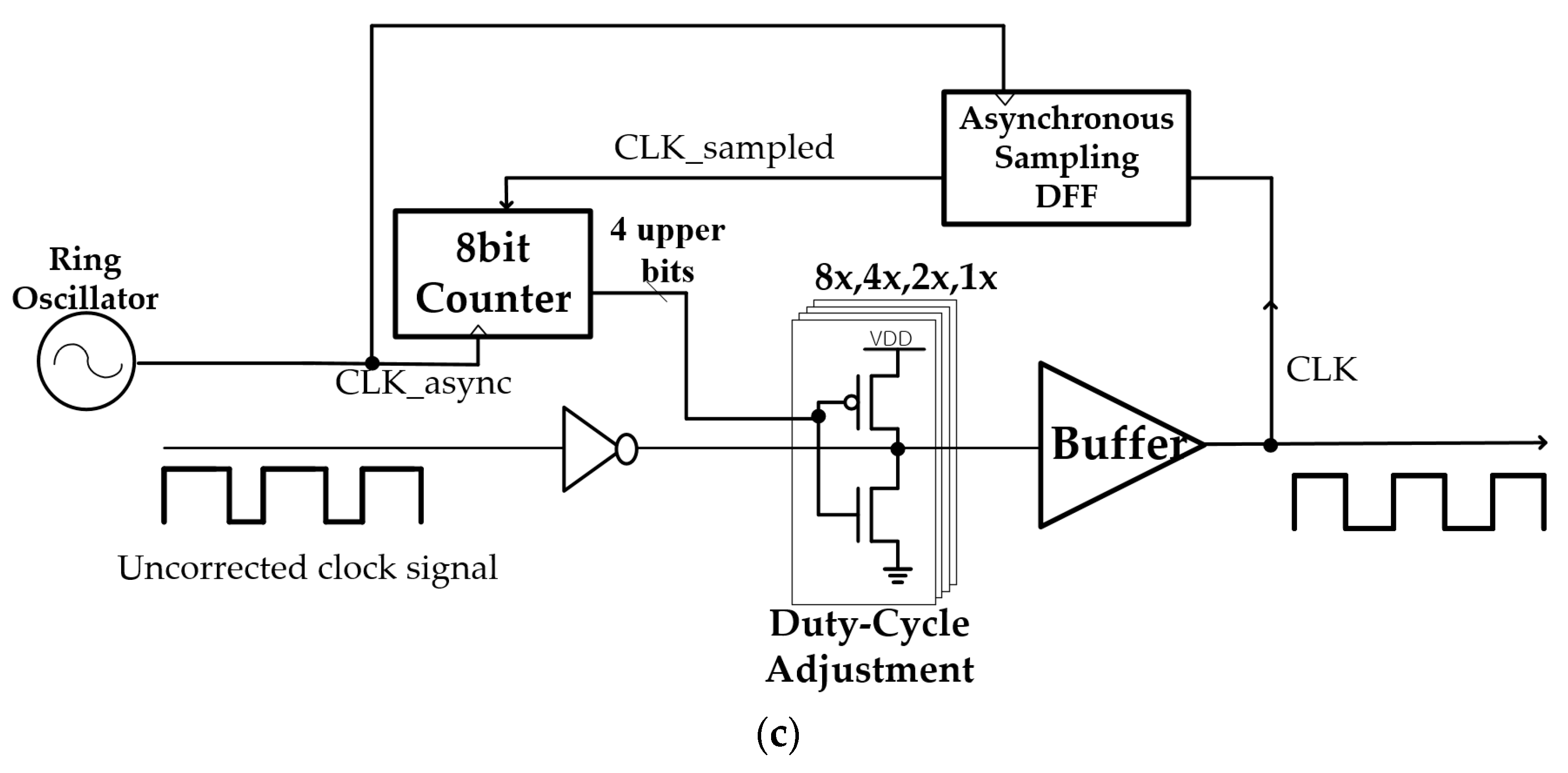
The transient characteristic of the asynchronous sampling system is illustrated in Figure 1b. As shown in the figure, CLK is down-converted with time-varying frequencies and duty cycles. Although CLK_sampled has transient fluctuations in its duty cycle, it should be noted that the average voltage of CLK_sampled follows the average voltage of CLK in the long run. Therefore, the duty distortion of CLK can be measured simply by measuring the average voltage of CLK_sampled, as the average value of CLK_sampled should settle in 0.5∙VDD when the duty cycle of CLK is 50% (no distortion). By utilizing this observation, we implemented an asynchronous sampling duty cycle corrector (AS−DCC), the structure of which is depicted in Figure 1c. Asynchronous sampling DFF extracts the duty cycle information of the clock (CLK) and counter changes the code according to the CLK_sampled (the output of the DFF). Duty-cycle adjustment, which is operated from the code of the counter, corrects the duty cycle of the uncorrected clock input by controlling pull-up or pull-down of transistors. For example, if the duty of the input clock was 60%, on average, 6 out of 10 asynchronously sampled values (CLK_sampled) would be 1. Six 1 s and four 0 s increase the counter value (6 times up, and 4 times down), which sets the duty in a direction close to 50%, by strengthening the nmos of the duty-cycle adjustment. Thus, the duty cycle is corrected to 50%. The counter is made using only the upper 4 bits so that the duty errors according to PVT variations in a clock generator would be covered not only without an overflow of the counter but also causing fewer errors than 1%. Moreover, additional 4LSB-bits should be created to minimize frequent duty changes with minimal area and power consumption. As long as the frequency of the oscillator used for asynchronous sampling is slow enough to operate the counter, it does not matter which frequency it is, so there is no special architecture to tune the oscillation frequency. Therefore, the frequency of the oscillator is set to be less than 100 MHz to minimize power consumption. The settling time of the proposed AS−DCC architecture primarily depends on N in (1) because a smaller value of Tasync implies a faster extraction of duty information by the asynchronous sampling D-flip-flop. In addition, the number of bits in the counter also affects the transient settling response, as smaller counter bits mean faster updates of the input bits for the duty-cycle adjustment block. However, as the counter must properly suppress transient fluctuations, there is a trade-off relationship between settling time and transient fluctuation in terms of the number of counter bits. The amount of transient fluctuations is severely affected also by the value of α, as revealed from the in-depth analysis in the next session, which requires an additional control scheme (as shown in Section 4) to reduce the impact of α on the duty cycle fluctuation and relax design constraint on the counter bits and settling time.

3. Analysis on Asynchronous Sampling

3.1. Settling Requirements

As mentioned in Section 2, the AS−DCC’s response is severely affected by the frequency−relations between CLK and CLK_async. This characteristic could make the AS−DCC malfunction in some undesired conditions, producing transient duty cycle fluctuations at the clock output of AS−DCC. Figure 2 shows one example case where the AS−DCC does not capture and compensate the duty cycle errors adequately when α is very small (the frequency of CLK is very close to one of harmonics of CLK_async). In this case, the asynchronous sampling D flip-flop keeps sampling consecutive 1 s or 0 s, which generates a burst of output bits of the same value. As these long consecutive patterns are difficult to suppress using practical filters or counters, they may produce large transient fluctuations in the counter output (and the resulting duty cycle of the output clock). Therefore, if possible, α should be controlled not to have small value, thus avoiding a quasi-harmonic relationship between CLK and CLK_async.
In addition to the quasi-harmonic case (α is too small), when α is very close to a fractional number with an odd denominator, the AS−DCC may produce similar unstable transient responses as well. This is because the sampling DFF samples identical values, as in the previous case, if the frequency of CLK and its associated value of α meets the odd-denominator condition. For example, in Figure 3a, the duty cycle of the CLK_sampled shows a long pattern of ~66.7% duty cycle (and then a long pattern of ~33.3% duty cycle) even if the input CLK has a perfect 50% duty cycle when α is very close to 1/3, which makes the output of the counter continually build up in one direction for a long duration. A similar phenomenon, in which the duty cycle is not settled and keeps changing over time, is called transient duty cycle fluctuation in this paper. In order to avoid this problem, the value of α should have enough offset from any fractional numbers with an odd denominator. It should be noted that the AS−DCC does not have the problem for even denominators, as shown in Figure 3b. This is because, in the even-denominator conditions, 1 s and 0 s are sampled at the same rate with the duty cycle of CLK, without producing such long consecutive bursts of identical bits. This difference is evident when comparing the counter values, as seen in Figure 3a,b. The counter value in Figure 3a continues to increase, while the counter in Figure 3b maintains the same value over time.
In order to perform further analysis on the transient responses of the AS−DCC in such conditions (α is very close to a fractional number), we re-expressed the α term in the previous Equation (1) with additional integer and residual terms as follows:
α = k / o + β   ( o   is   odd   number ,   k   is   positive   integer   less   than   o ,   β 0 )
α = k / e + β   ( e   is   even   number ,   k   is   positive   integer   less   than   e ,   β 0 )
The integer numbers k, o, and e in (2) and (3) are introduced to represent the α term with respect to a fractional number with odd/even denominators, respectively. As the α term itself is a fractional number smaller than 1, k should be smaller than the denominators (o and e) for both cases. β stands for the residual offset from the fractional number. In other words, a smaller value of β in (2) indicates that the value of α is located very close to a fraction with an odd denominator. In that condition, the AS−DCC may suffer from the large fluctuation condition (typically when β is less than 0.01), which is characterized by the following mathematical derivations and simulations.
In order to find out the response of the AS−DCC for various values of k, o, e, and β, we converted a simplified simulation model of the AS−DCC in Figure 1c, by converting the counter to a charge pump followed by a capacitor for accumulation to see the tendency of the DCC circuit without any quantization errors. A larger number of counter bits means a larger capacitor, and the fluctuations at the counter output (which is proportional to the transient fluctuation in the duty-cycle of CLK) are modeled by the voltage fluctuation at the charge-pump output. The equivalent circuit model for the AS−DCC is simulated across various values of k and β when o = 5, in order to find out the transient characteristics of the AS−DCC in the odd-denominator conditions. In Figure 4a, the normalized ΔV corresponds to the peak-to-peak voltage fluctuation at the charge pump output of the loop filter (which is related to the duty-cycle fluctuation of CLK). Mathematically, the peak-to-peak voltage variations are estimated by the following equations.
Floor (   T c l k 2 ( o 1 ) 2 T c l k o ( o 1 ) 2 β T c l k o β T c l k + 1 )   =   O ( o ,   β )
Δ V = I Δ t C
Δ V   =   I × T a s y n c   C × O ( o ,   β )
In the equations above, O(o, β) denotes the maximum accumulation of identical values in the counter when the first rising edges of the CLK and CLK_async start at the same time. For example, when o = 5, the third sampling point contributes to the increase or decrease in the counter output, as illustrated in Figure 4d. Therefore, the time range when the counter accumulates in one direction is given by the following expression:
T accum = T c l k 2 ( o 1 ) 2 T c l k o ( o 1 ) 2 β T c l k   =   T c l k 2 ( o 1 ) 2 T a s y n c
Because the (o + 1)/2 th sampling point (3rd sampling point in Figure 4d) contributes to the accumulation of the counter, the time range which the (o + 1)/2 th sampling point can sample 1 is limited to Taccum when the duty of the clock is 50%. Afterwards, Taccum should be divided by o · β · Tclk because the sampling clock shifts by this amount compared to the previous sampling point after o · Tasync (= o ·(N + k/o + β) ·Tclk) seconds. For example, after CLK_async samples the 3rd point, the 8th sampling point relatively moves by 5 · β · Tclk after 5 · Tasync seconds. The actual move from the 3rd sampling point to the 8th sampling point is (5N + k + 5β) · Tclk, but 5N + k can be ignored in the calculation because it is an integer number. In addition, it should be noted that the value of ΔV is not affected by k but β, which is verified with simulation results in Figure 4b.
In Figure 4a, ΔV is normalized for fair comparisons to remove its dependency on N and α to characterize the dependency of ΔV on β. The shape of the theoretical curve in Figure 4b turned out to be similar to that of the odd-denominator cases, and they show almost identical voltage variations for the same value of β. Therefore, from the mathematical analysis and simulation results, we can conclude that voltage variations are not related to the value of k and have a symmetrical distribution with respect to β. On the other hand, as shown in Figure 4c, in the vicinity of even denominators, smaller voltage fluctuations (and therefore smaller duty-cycle distortions) are observed than in the odd-denominator cases, and the fluctuations actually present within the stable range which is defined in the next section.

3.2. Verification with Behaviroal Simulations

To verify Equation (4) in more realistic situations and counter designs, behavioral simulations with Verilog models are performed. The simulation conditions are given as follows: (1) The first rising edges of the CLK and CLK_async rise at the same time. (2) An 8-bit counter which is initialized to 8′b1000_1000 is used to accumulate the output of asynchronous sampling block, of which upper 4-bits are used to control the duty cycle.
The theoretical digital code variations are calculated with Equation (4) and compared with the simulation results. To calculate the range of β which is out of oscillating codes, Equation (4) is switched to (8) because the operator ‘floor’ needs to be taken out from Equation (4) to consider the worst case. O(o, β) and O′(o, β) do not represent different meanings, but O(o, β) is changed to O′(o, β) for simplicity and accuracy of the calculation.
T c l k 2 ( o 1 ) 2 T c l k o ( o 1 ) 2 β T c l k o β T c l k + 1   =   O ( o ,   β )
O ( o ,   β ) + 1     7 ( o 1 ) 2 .
Equation (9) is derived from the following process. Since the counter code is reset to 10001000, the upper 4-bits of the counter code (the counter’s output) change after the counter receives eight ones, which means the counter’s output remains stationary until it receives seven (net) ones or zeros. In the odd-denominator case, after O(o, β) · o · Tasync seconds, the net accumulation value in the counter code is (o − 1)/2 (or −(o − 1)/2 depending on the initial phase relationship between CLK and CLK_async) due to the asymmetric sampling in the odd denominator in α.
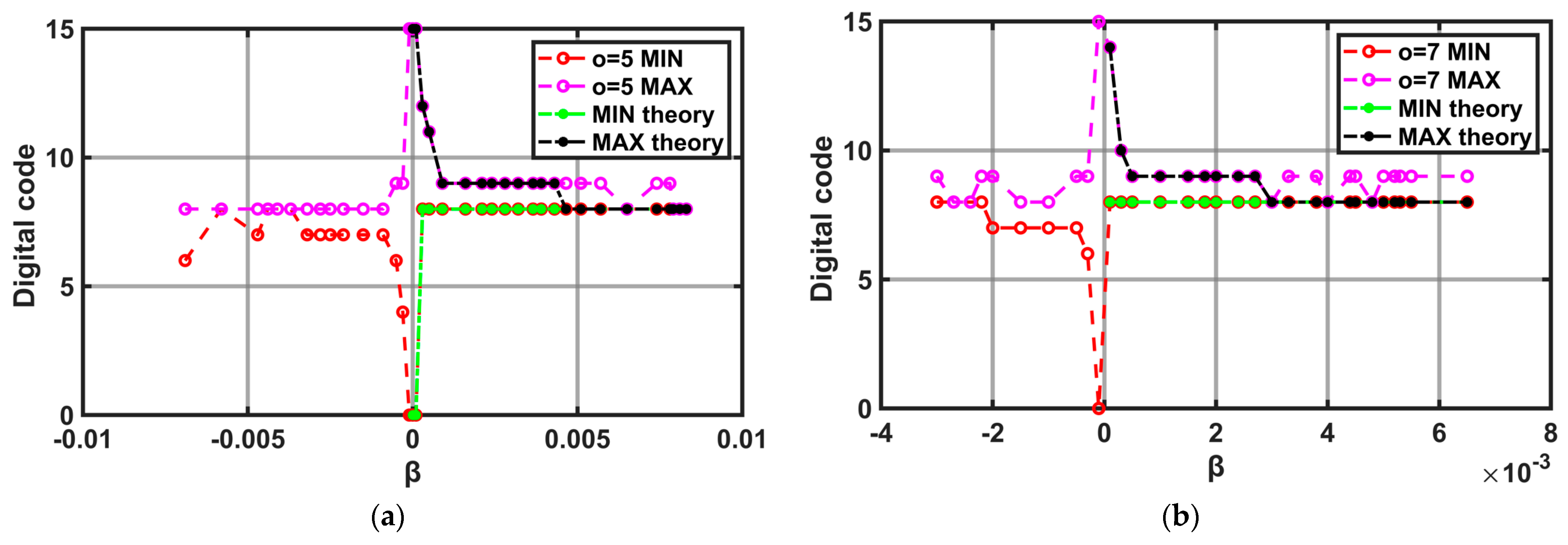
The value of β should be chosen so that the inequality in (9) holds to prevent the counter update. From Equation (8), to prevent the unintentional update of the counter output due to the consecutive 1 s or 0 s, β should be larger than 0.00455 when o = 5, and β should be larger than 0.002977 when o = 7. Figure 5a–c show the peak-to-peak variations of the upper 4 bits in the counter code (which is the output of the counter) in some odd-denominator conditions (o = 5 and 7) and an even-denominator condition (e = 4) respectively. Similar to the result of Section 3.1, when the value β is very small near old-denominator conditions, it can be seen that the counter code moves largely from 4′b0000 to 4′b1111 without being settled, which prevents the DCC from operating properly. In addition, the even-denominator condition shows that the overall counter code does not change when the input duty cycle of the clock is 50%, regardless of the beta value, which indicates that the DCC operates properly. The shape of the theoretical curve turns out to be similar to those from simulations when β is very small, but as β grows larger, deviations of simulation results from the mathematical derivations are observed, as the basic assumption on the odd/even-denominator conditions (β is very small) does not hold anymore.
Equation (10) is a generalized version of (9), assuming the least m bits of the counter code are trimmed for deriving the counter output. Because increasing the number unused bits for duty control does not affect any other conditions, Equation (10) can be made by changing the margin (from 7 to 2m1), which is needed to prevent an unintentional update of upper bits of the counter output.
O ( o ,   β ) + 1     2 m 1 1 ( o 1 ) 2 .

4. Design Example

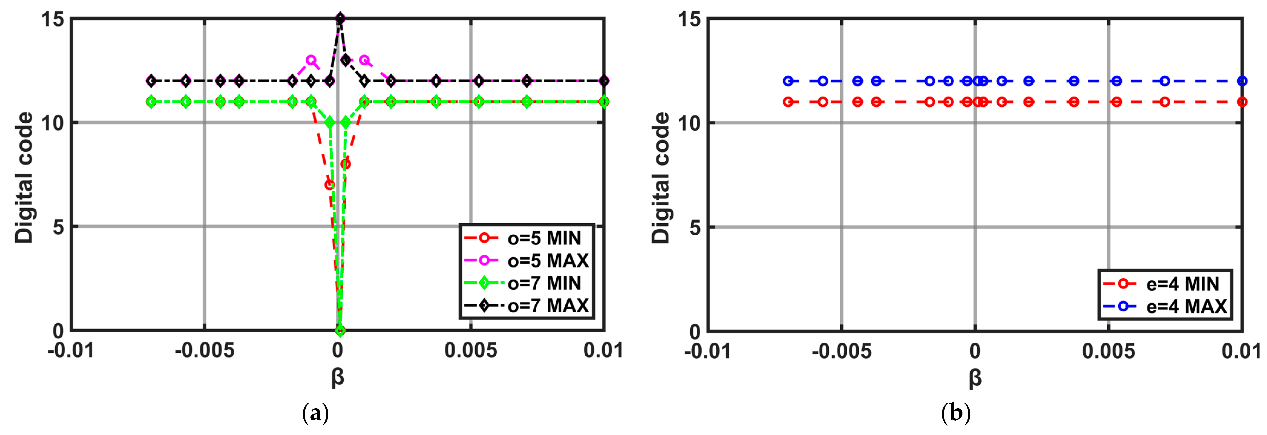
When the proposed AS−DCC, as shown in Figure 1c, is implemented with the 8-bit counter which is used in Verilog simulations in the previous session, the quantization errors due to the finite resolution of the counter cause 1-bit toggling of output bits in stable conditions. Clock signals created by the clock generator were passed through the AS−DCC to see how the counter works during the proposed AS−DCC process. Figure 6 shows the maximum and minimum digital code of the 4 MSBs of the 8-bit counter in the proposed AS−DCC in steady states. If the difference between the maximum and minimum counter output is 1, the observation implies that the output is toggling between two adjacent values (1-bit toggling). In Figure 6a, the maximum and minimum values of the counter are measured in two odd-denominator conditions across various values of β. It turns out that the output toggles more than two when the AS−DCC enters the unstable region, while the output toggles just 1-bit entering stable regions. The counter bit toggles 1-bit when the AS−DCC is operating in even-denominator conditions, as shown in Figure 6b, as the AS−DCC operates in stable conditions in the even-denominator condition, as investigated in Section 3.
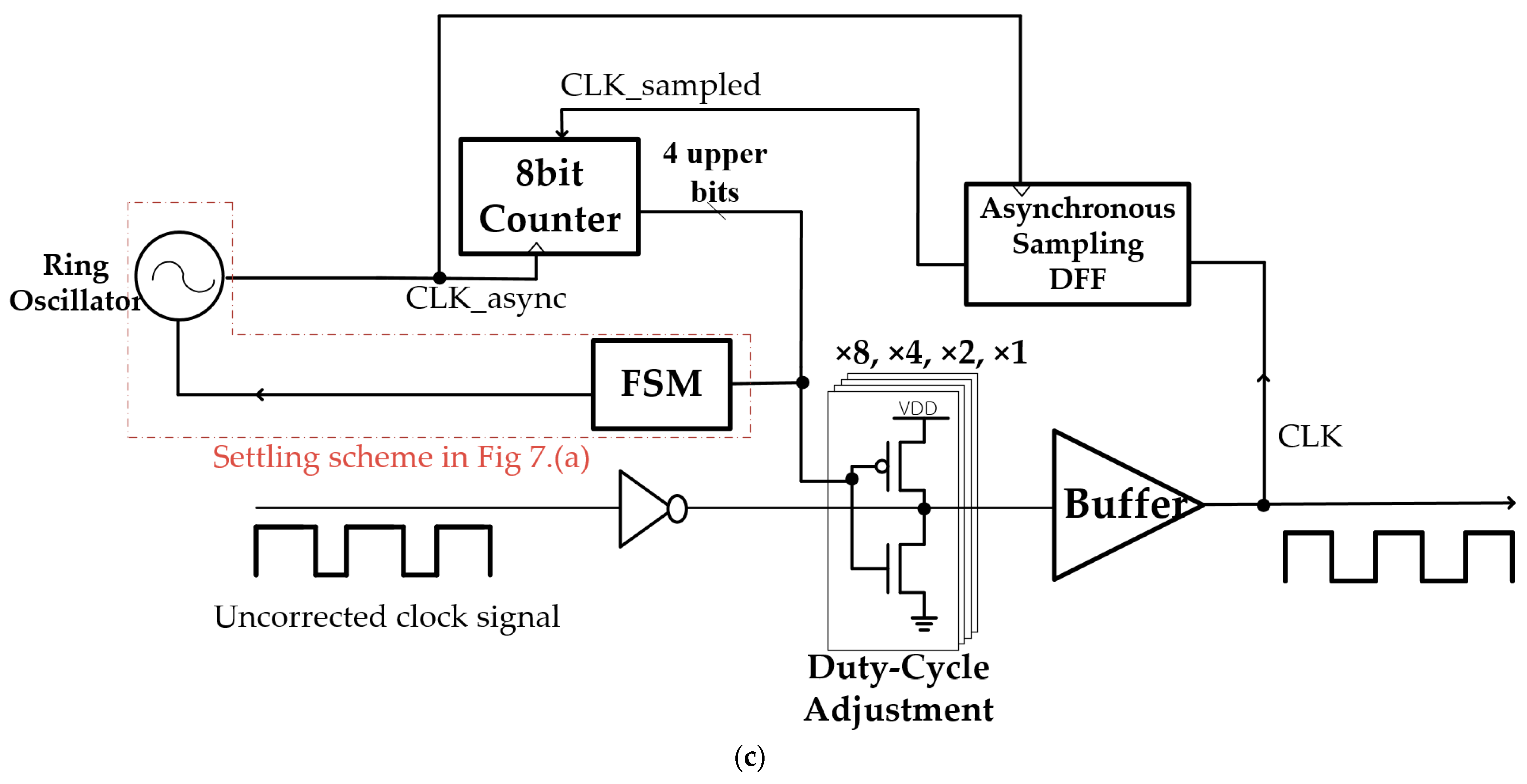
The observation that the AS−DCC’s counter output will toggle between two adjacent values is utilized to detect the operating condition of the AS−DCC and avoid its operation in unstable conditions; however, if the AS−DCC’s counter digital code changes by more than 2 bits, this implies that the AS−DCC is operating in an unstable condition. By using the algorithm presented in Figure 7a, the AS−DCC’s operating condition can then be changed by slowing down the oscillator frequency for Tasync to avoid the operation falling in the unstable condition. As shown in Figure 7c, the FSM detects unstable settling conditions and slows down the oscillator. To verify this algorithm in terms of simulation, the simulation was performed by reducing the oscillator frequency when more than 1 bit of toggling was detected. Figure 7b shows a post-layout simulation result of the duty cycle changes of the output of the proposed AS−DCC operating before and after applying the algorithm. The initial operation condition for the simulation is given by Tasync = 520.0217 ps and Tclk = 100 ps, which means that the CLK_async is under the odd denominator of 5 because α = 0.200217 and β = 0.000217, hence the duty cycle oscillates from 47.5 to 51% without applying the control scheme, as shown in Figure 7b. After the control scheme is turned on, however, Tasync is increased to Tasync = 520.8317 ps, which means that the value of β is increased from 0.000217 to 0.008317. According to Figure 6a, 0.008317 is big enough to deviate from the odd-denominator condition. As a result, the AS−DCC escapes out of the unstable condition and the duty cycle toggles only between 49.5 and 50%.
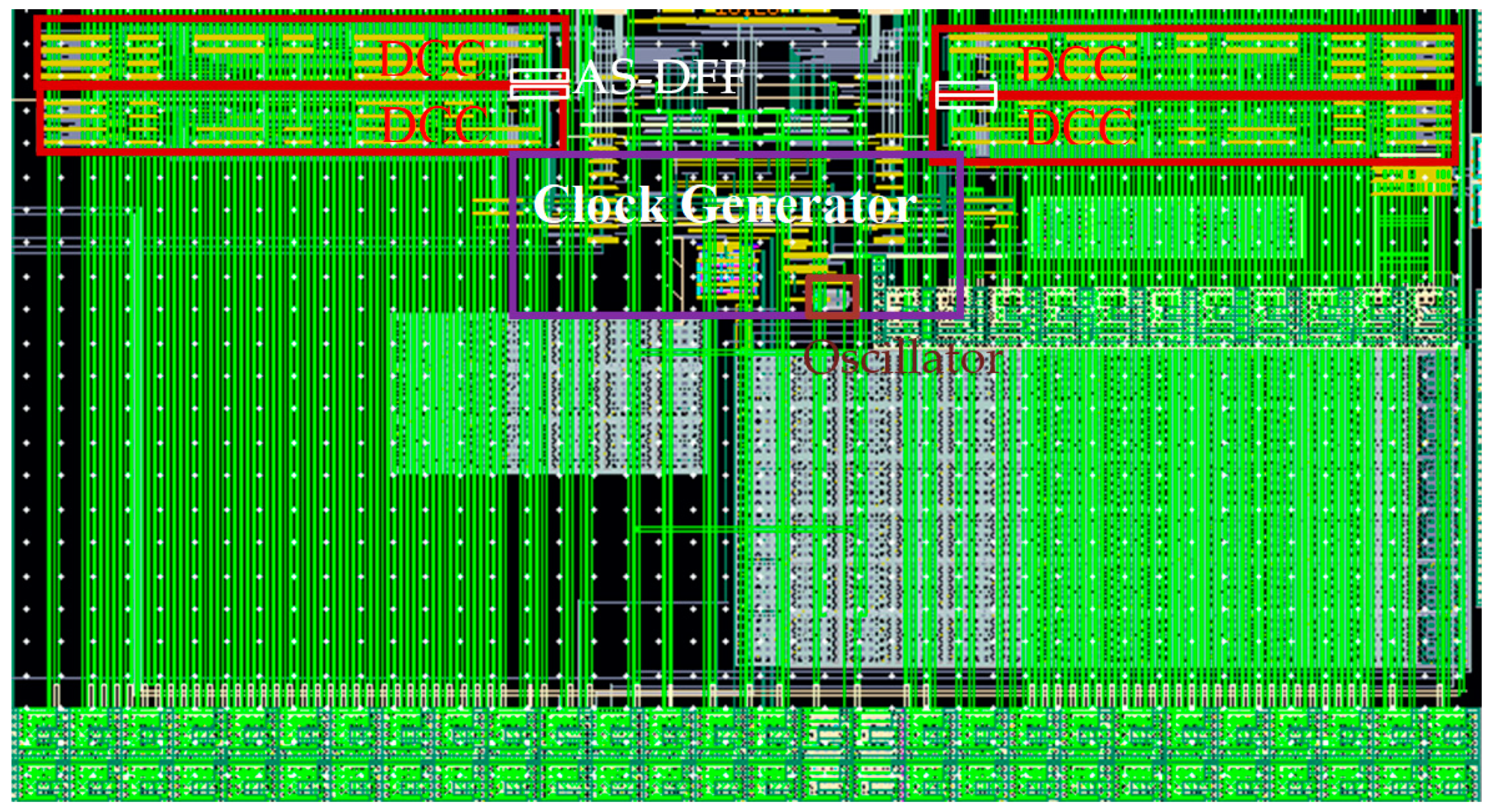
The proposed AS−DCC is designed in a 40-nm CMOS process, occupying an area of 0.0082 mm2 including a clock generator (Figure 8). It consumes 530 uW per one DCC with 1 V supply voltage when the frequency of CLK is 8 GHz and that of CLK_async is about 88.24 MHz in post-layout simulation. The maximum duty-cycle error at the output in the range 4 GHz to 8 GHz is measured to be lower than 0.8°, which is a very small error.
Table 1 shows a comparison with previous studies. The proposed circuit operates at a high-frequency range, not only without occupying a large area, but also consuming less power compared to other circuits.

5. Conclusions

This paper presents a method to prevent and escape the unstable state of asynchronous sampling to properly apply the asynchronous algorithm to correct the duty cycle of high-frequency clocks. Theoretical analysis and estimation of the duty cycle oscillation condition are performed along with post-layout simulations verifying the analysis. The post-layout simulations following the Verilog simulations for digital-level verifications in Section 3 and Section 4 show good agreement with the theoretical predictions.

Author Contributions

Conceptualization, G.P. and W.B.; methodology, G.P. and W.B.; software, G.P.; validation, G.P., W.B. and J.H.; formal analysis, G.P. and W.B.; investigation, G.P. and W.B.; data curation, G.P.; writing—original draft preparation, G.P.; writing—review and editing, W.B. and J.H.; visualization, G.P.; supervision, W.B. and J.H.; project administration, W.B. and J.H; funding acquisition, J.H. All authors have read and agreed to the published version of the manuscript.

Funding

This research received no external funding.

Data Availability Statement

Data sharing is not applicable to this article.

Acknowledgments

The research was sponsored in part by Samsung Research Funding & Incubation Center of Samsung Electronics under Project Number SRFC-IT2001-02 and the National Research Foundation of Korea (NRF) grant funded by the Korean government (MSIT) (No. 2021R1C1C1003634).

Conflicts of Interest

The authors declare no conflict of interest.

References

  1. Lin, Y.-T.; Chen, W.-Z. A 50 Gb/s PAM-4 Transmitter with feedforward equalizer and background phase error calibration. In Proceedings of the 2020 IEEE Asian Solid-State Circuits Conference (A-SSCC), Virtual, 9–10 November 2020; pp. 1–2. [Google Scholar] [CrossRef]
  2. Vazgen, M.-S.; Arman, A.-A.; Manvel, G.-T.; Hakob, K.-T.; Karo, S.-H.; Ruben, M.-H. Duty-cycle correction circuit for high speed interfaces. In Proceedings of the 2019 IEEE 39th International Conference on Electronics and Nanotechnology (ELNANO), Kyiv, Ukraine, 16–18 April 2019; pp. 42–45. [Google Scholar]
  3. SR, J.P.; Hiremath, S.S. Dual loop clock duty cycle corrector for high speed serial interface. In Proceedings of the 2017 International Conference on Smart Technologies for Smart Nation (SmartTechCon), Bengaluru, India, 17–19 August 2017; pp. 935–939. [Google Scholar] [CrossRef]
  4. Jeong, C.-H.; Abdullah, A.; Min, Y.-J.; Hwang, I.-C.; Kim, S.-W. All-digital duty-cycle corrector with a wide duty correction range for DRAM applications. IEEE Trans. Very Large Scale Integr. (VLSI) Syst. 2016, 24, 363–367. [Google Scholar] [CrossRef]
  5. Chen, P.; Chen, S.-W.; Lai, J.-S. A low power wide tange duty cycle corrector based on pulse shrinking/stretching mechanism. In Proceedings of the 2007 IEEE Asian Solid-State Circuits Conference, Jeju, Korea, 12–14 November 2007; pp. 460–463. [Google Scholar] [CrossRef]
  6. Chung, C.-C.; Sheng, D.; Li, C.-J. A Wide-range low-cost all-digital duty-cycle corrector. IEEE Trans. Very Large Scale Integr. (VLSI) Syst. 2014, 23, 2487–2496. [Google Scholar] [CrossRef]
  7. Wei, S.-N.; Wang, Y.-M.; Peng, J.-H.; Surya, Y. A range extending delay-recycled clock skew-compensation and/or duty-cycle-correction circuit. In Proceedings of the Technical Program of 2012 VLSI Design, Automation and Test, Hsinchu, Taiwan, 23–25 April 2012; pp. 1–4. [Google Scholar] [CrossRef]
  8. Han, S.-R.; Liu, S.-I. A 500-MHz–1.25-GHz Fast-Locking Pulsewidth Control Loop with Presettable Duty Cycle. IEEE J. Solid-State Circuits 2004, 39, 463–468. [Google Scholar] [CrossRef]
  9. Shin, N.; Song, J.; Chae, H.; Kim, C. A 7 ps Jitter 0.053 mm2 Fast Lock All-Digital DLL With a Wide Range and High Resolution DCC. IEEE J. Solid-State Circuits 2009, 44, 2437–2451. [Google Scholar] [CrossRef]
  10. Kang, K.-T.; Kim, S.-Y.; Kim, S.J.; Lee, D.; Yoo, S.-S.; Lee, K.-Y. A 0.33–1 GHz Open-Loop Duty Cycle Corrector with Digital Falling Edge Modulator. IEEE Trans. Circuits Syst. II Express Briefs 2018, 65, 1949–1953. [Google Scholar] [CrossRef]
  11. Min, Y.-J.; Jeong, C.-H.; Kim, K.-Y.; Choi, W.H.; Son, J.-P.; Kim, C.; Kim, S.-W. A 0.31–1 GHz Fast-Corrected Duty-Cycle Corrector with Successive Approximation Register for DDR DRAM Applications. IEEE Trans. Very Large Scale Integr. (VLSI) Syst. 2012, 20, 1524–1528. [Google Scholar] [CrossRef]
  12. Agarwal, K.B.; Montoye, R.K. A Duty-cycle correction circuit for high-frequency clocks. In Proceedings of the 2006 Symposium on VLSI Circuits, 2006. Digest of Technical Papers, Honolulu, HI, USA, 15–17 June 2006. [Google Scholar] [CrossRef]
  13. Cheng, K.-H.; Su, C.-W.; Chang, K.-F. A High Linearity, Fast-Locking Pulsewidth Control Loop with Digitally Programmable Duty Cycle Correction for Wide Range Operation. IEEE J. Solid-State Circuits 2008, 43, 399–413. [Google Scholar] [CrossRef]
  14. Zuo, S.; Zhao, J.; Zhou, Y. A 2.1 GHz, 210 μW, —189 dBc/Hz DCO with Ultra Low Power DCC Scheme. Electronics 2021, 10, 805. [Google Scholar] [CrossRef]
  15. Su, J.-R.; Liao, T.-W.; Hung, C.-C. Delay-line based fast-locking all-digital pulsewidth-control circuit with programmable duty cycle. In Proceedings of the IEEE Asian Solid State Circuits Conference (A-SSCC), Kobe, Japan, 12–14 November 2012; pp. 305–308. [Google Scholar] [CrossRef]
  16. Kao, S.-K. A 6-Locking Cycles All-Digital Duty Cycle Corrector with Synchronous Input Clock. Electronics 2021, 10, 860. [Google Scholar] [CrossRef]
  17. Kao, S.-K. Design and Implementation of Fast Locking All-Digital Duty Cycle Corrector Circuit with Wide Range Input Frequency. Electronics 2021, 10, 71. [Google Scholar] [CrossRef]
  18. Mansuri, M.; Jaussi, J.E.; Kennedy, J.T.; Hsueh, T.-C.; Shekhar, S.; Balamurugan, G.; O’Mahony, F.; Roberts, C.; Mooney, R.; Casper, B. A Scalable 0.128–1 Tb/s, 0.8–2.6 pJ/bit, 64-Lane Parallel I/O in 32-nm CMOS. IEEE J. Solid-State Circuits 2013, 48, 3229–3242. [Google Scholar] [CrossRef]
  19. Bae, W. Frequency acquisition technique for injection-locked clock generator using asynchronous-sampling frequency detection. Electron. Lett. 2017, 53, 1240–1242. [Google Scholar] [CrossRef]
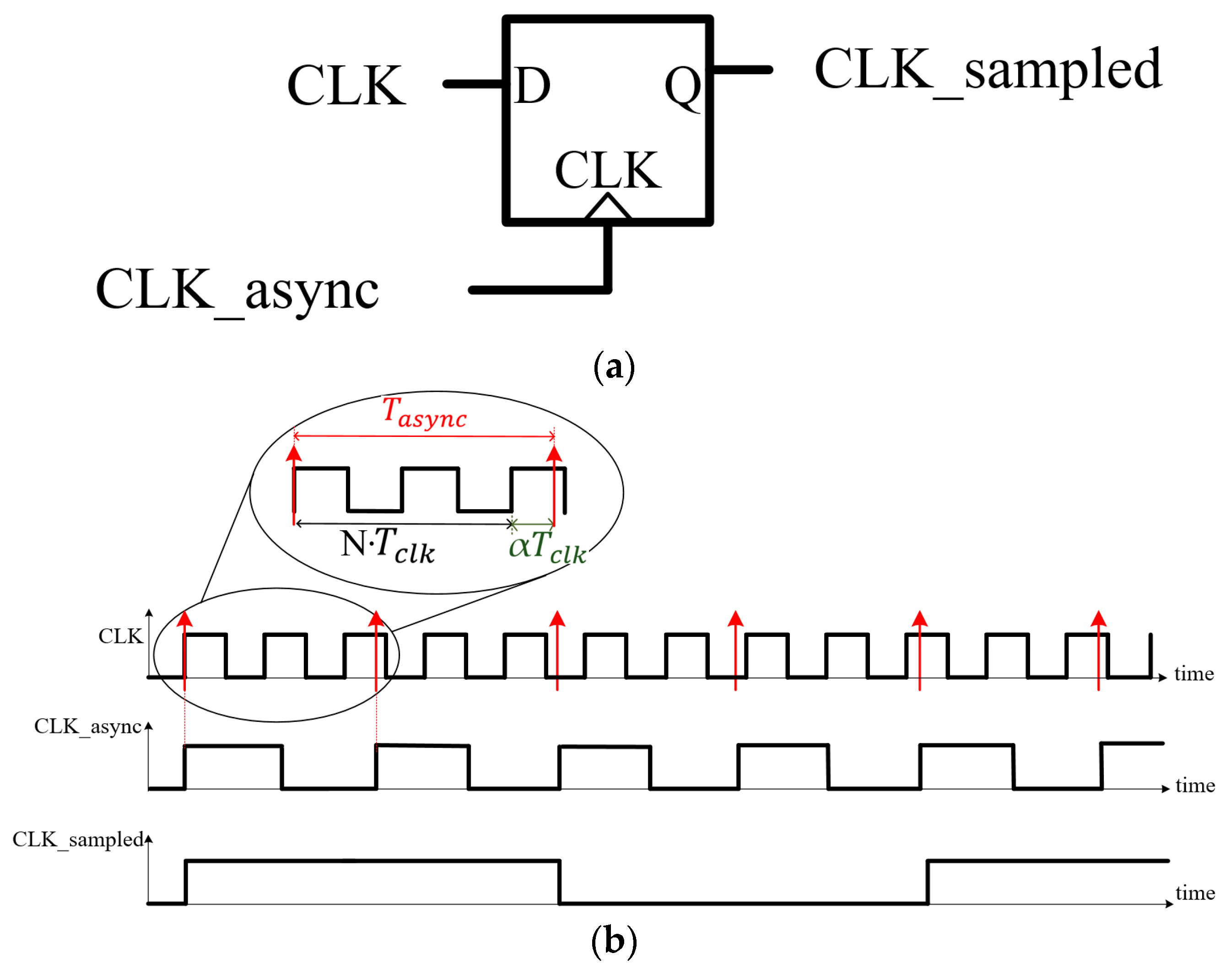
Figure 1. (a) Asynchronous sampling scheme using D-flip-flop. (b) An example timing diagram of asynchronous sampling, assuming N = 2, α = 0.29. (c) Schematic of AS−DCC.
Electronics 10 02594 g001aElectronics 10 02594 g001b
Figure 2. Timing diagram of asynchronous sampling when N = 2 and α << 1 (the frequency of CLK is very close to the second harmonic of CLK_async).
Electronics 10 02594 g002
Figure 3. Timing diagrams of asynchronous sampling when α << 1, (a) α ≈ 1/3 (the odd-denominator case), and (b) α ≈ ¼ (the even-denominator case).
Electronics 10 02594 g003aElectronics 10 02594 g003b
Figure 4. (a) Structure of a model of AS−DCC for measuring voltage variations. (b) Simulated and calculated peak−to−peak voltage variations for an odd−denominator condition (o = 5). (c) Simulated voltage variations according to odd and even denominators in α. (d) Timing diagram when o = 5, and α = 2/5 + β (red arrows indicate the rising edges of CLK_async).
Electronics 10 02594 g004
Figure 5. (a) Maximum and minimum digital code of the Verilog simulations and theoretical results in an odd-denominator condition (o = 5). (b) Maximum and minimum digital code of the Verilog simulations and theoretical results when o = 7. (c) Maximum and minimum digital code of the Verilog simulations and theoretical results in an even-denominator condition (e = 4).
Electronics 10 02594 g005aElectronics 10 02594 g005b
Figure 6. (a) Maximum and minimum digital code of the DCC counter when the denominator value of o is 5 and 7. (b) Maximum and minimum digital code of the DCC counter when the denominator value of e is 4.
Electronics 10 02594 g006
Figure 7. (a) Asynchronous sampling settling scheme. (b) The change of the duty cycle before and after the scheme turns on. (c) Asynchronous sampling duty cycle corrector with the settling scheme.
Electronics 10 02594 g007aElectronics 10 02594 g007b
Figure 8. Layout of the proposed AS−DCC.
Electronics 10 02594 g008
Table 1. Performance comparison.
[10][15]This Work
Process55 nm180 nm40 nm
Operating frequency (GHz)0.333~10.2~0.64~8
Output duty cycle error (%)±2±2.5±0.8
Area (mm2)0.01860.02520.0082
Power consumption2.09 mW
@1 GHz
5.49 mW
@600 MHz
4.7 mW
@8 GHz
Publisher’s Note: MDPI stays neutral with regard to jurisdictional claims in published maps and institutional affiliations.