
Inkjet-Printed Molybdenum Disulfide and Nitrogen-Doped Graphene Active Layer High On/Off Ratio Transistors


Abstract
:1. Introduction
2. Results
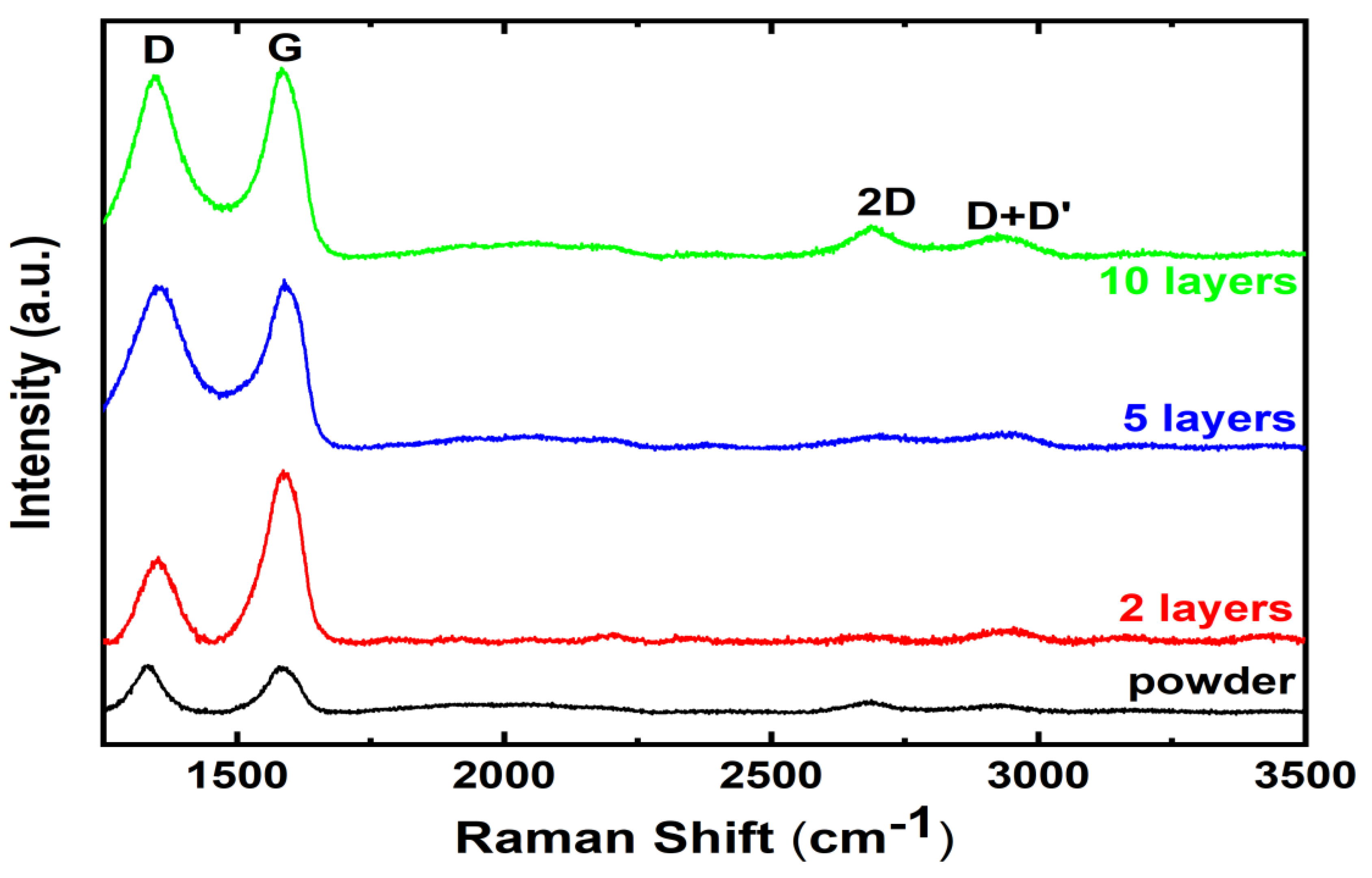
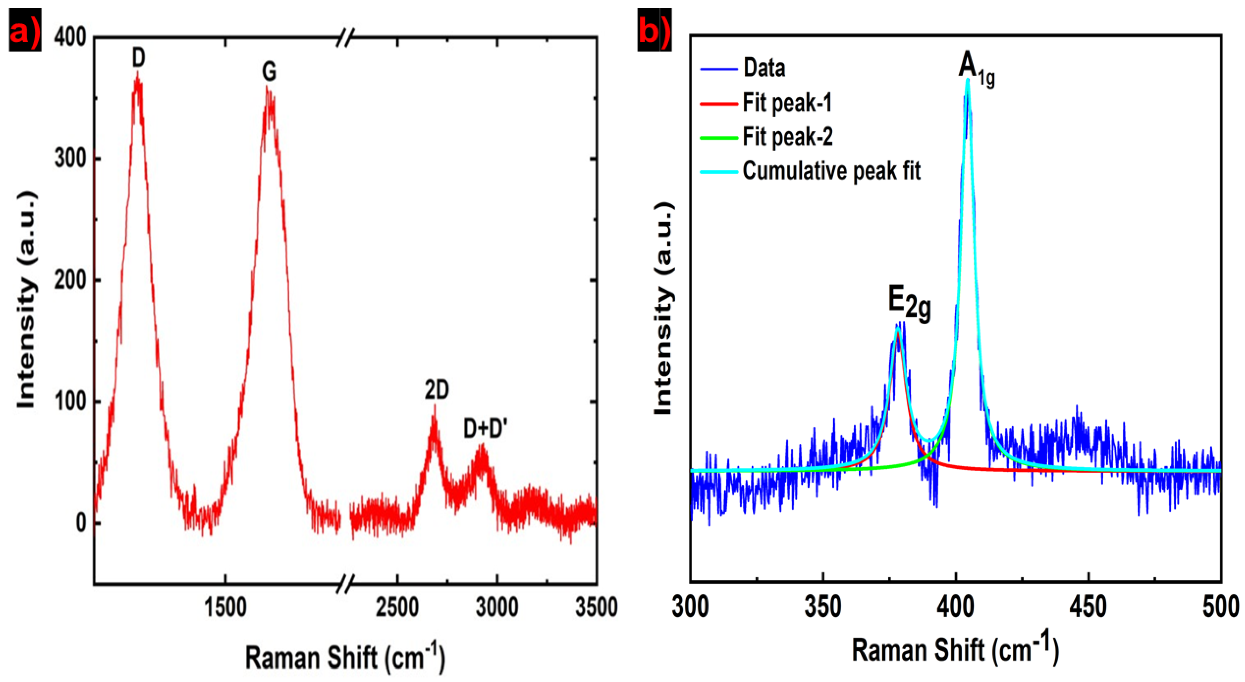
2.1. NDG and MoS2 Nanosheets
2.2. Printable Inks and Thin Films
2.3. MoS2–NDG Stack
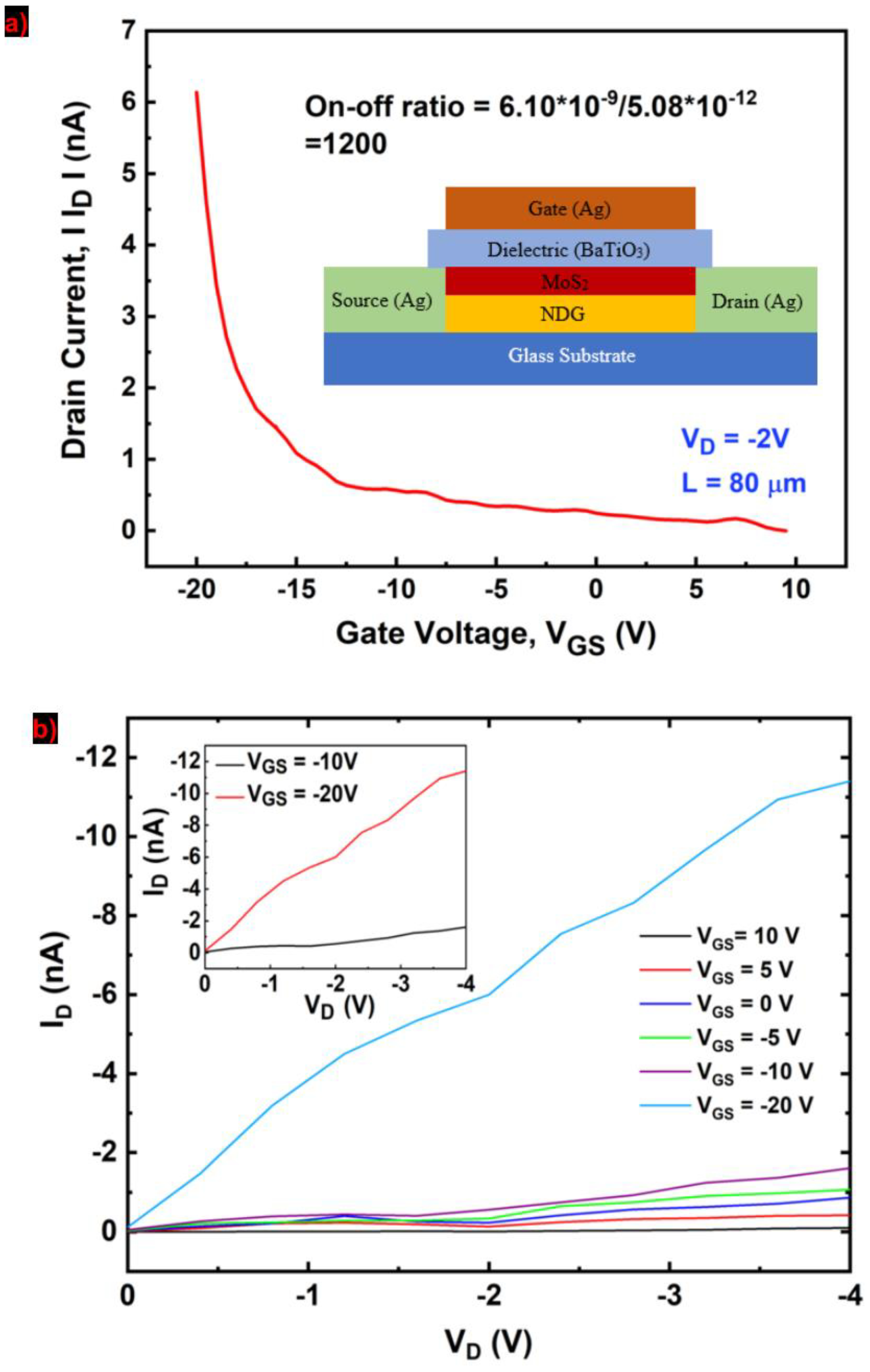
2.4. Transistor Fabrication and Characterization
3. Discussion
4. Materials and Methods
5. Summary
Supplementary Materials
Author Contributions
Funding
Conflicts of Interest
References
- Geim, A.K.; Novoselov, K.S. The rise of graphene. Nat. Mater. 2007, 6, 183–191. [Google Scholar] [CrossRef] [PubMed]
- Li, J.; Ye, F.; Vaziri, S.; Muhammed, M.; Lemme, M.C.; Östling, M. Efficient inkjet printing of graphene. Adv. Mater. 2013, 25, 3985–3992. [Google Scholar] [CrossRef] [PubMed]
- Xia, F.; Farmer, D.B.; Lin, Y.; Avouris, P. Graphene field-effect transistors with high on/off current ratio and large transport band gap at room temperature. Nano Lett. 2010, 10, 715–718. [Google Scholar] [CrossRef] [PubMed] [Green Version]
- Schwierz, F. Graphene transistors. Nat. Nanotechnol. 2010, 5, 487–496. [Google Scholar] [CrossRef]
- Torrisi, F.; Hasan, T.; Wu, W.; Sun, Z.; Lombardo, A.; Kulmala, T.S.; Hsieh, G.-W.; Jung, S.; Bonaccorso, F.; Paul, P.J. Inkjet-printed graphene electronics. ACS Nano 2012, 6, 2992–3006. [Google Scholar] [CrossRef]
- Carey, T.; Cacovich, S.; Divitini, G.; Ren, J.; Mansouri, A.; Kim, J.M.; Wang, C.; Ducati, C.; Sordan, R.; Torrisi, F. Fully inkjet-printed two-dimensional material field-effect heterojunctions for wearable and textile electronics. Nat. Commun. 2017, 8, 1202. [Google Scholar] [CrossRef] [Green Version]
- Li, X.; Zhu, H. Two-dimensional MoS2: Properties, preparation, and applications. J. Mater. 2015, 1, 33–44. [Google Scholar] [CrossRef] [Green Version]
- Coleman, J.N.; Lotya, M.; O’Neill, A.; Bergin, S.D.; King, P.J.; Khan, U.; Young, K.; Gaucher, A.; De, S.; Smith, R.J. Two-dimensional nanosheets produced by liquid exfoliation of layered materials. Science 2011, 331, 568–571. [Google Scholar] [CrossRef] [Green Version]
- Lee, K.; Kim, H.; Lotya, M.; Coleman, J.N.; Kim, G.; Duesberg, G.S. Electrical characteristics of molybdenum disulfide flakes produced by liquid exfoliation. Adv. Mater. 2011, 23, 4178–4182. [Google Scholar] [CrossRef]
- Li, J.; Naiini, M.M.; Vaziri, S.; Lemme, M.C.; Östling, M. Inkjet printing of MoS2. Adv. Funct. Mater. 2014, 24, 6524–6531. [Google Scholar] [CrossRef] [Green Version]
- He, Q.; Zeng, Z.; Yin, Z.; Li, H.; Wu, S.; Huang, X.; Zhang, H. Fabrication of flexible MoS2 thin-film transistor arrays for practical gas-sensing applications. Small 2012, 8, 2994–2999. [Google Scholar] [CrossRef]
- Kelly, A.G.; Hallam, T.; Backes, C.; Harvey, A.; Esmaeily, A.S.; Godwin, I.; Coelho, J.; Nicolosi, V.; Lauth, J.; Kulkarni, A. All-printed thin-film transistors from networks of liquid-exfoliated nanosheets. Science 2017, 356, 69–73. [Google Scholar] [CrossRef]
- Lin, Z.; Liu, Y.; Halim, U.; Ding, M.; Liu, Y.; Wang, Y.; Jia, C.; Chen, P.; Duan, X.; Wang, C. Solution-processable 2D semiconductors for high-performance large-area electronics. Nature 2018, 562, 254–258. [Google Scholar] [CrossRef] [PubMed]
- Zhou, S.Y.; Gweon, G.-H.; Fedorov, A.V.; First de, P.N.; De Heer, W.A.; Lee, D.-H.; Guinea, F.; Neto, A.H.C.; Lanzara, A. Substrate-induced bandgap opening in epitaxial graphene. Nat. Mater. 2007, 6, 770–775. [Google Scholar] [CrossRef] [PubMed] [Green Version]
- Lawlor, J.A.; Ferreira, M.S. Sublattice asymmetry of impurity doping in graphene: A review. Beilstein J. Nanotechnol. 2014, 5, 1210–1217. [Google Scholar] [CrossRef] [PubMed] [Green Version]
- Han, M.Y.; Özyilmaz, B.; Zhang, Y.; Kim, P. Energy bandgap engineering of graphene nanoribbons. Phys. Rev. Lett. 2007, 98, 206805. [Google Scholar] [CrossRef] [Green Version]
- Koh, Y.K.; Bae, M.-H.; Cahill, D.G.; Pop, E. Reliably counting atomic planes of few-layer graphene (n > 4). ACS Nano 2010, 5, 269–274. [Google Scholar] [CrossRef]
- Addou, R.; Colombo, L.; Wallace, R.M. Surface defects on natural MoS2. ACS Appl. Mater. Interfaces 2015, 7, 11921–11929. [Google Scholar] [CrossRef]
- Ferrari, A.C.; Meyer, J.C.; Scardaci, V.; Casiraghi, C.; Lazzeri, M.; Mauri, F.; Piscanec, S.; Jiang, D.; Novoselov, K.S.; Roth, S. Raman spectrum of graphene and graphene layers. Phys. Rev. Lett. 2006, 97, 187401. [Google Scholar] [CrossRef] [Green Version]
- Lu, Y.-F.; Lo, S.-T.; Lin, J.-C.; Zhang, W.; Lu, J.-Y.; Liu, F.-H.; Tseng, C.-M.; Lee, Y.-H.; Liang, C.-T.; Li, L.-J. Nitrogen-doped graphene sheets grown by chemical vapor deposition: Synthesis and influence of nitrogen impurities on carrier transport. ACS Nano 2013, 7, 6522–6532. [Google Scholar] [CrossRef] [Green Version]
- Hernandez, Y.; Nicolosi, V.; Lotya, M.; Blighe, F.M.; Sun, Z.; De, S.; McGovern, I.T.; Holland, B.; Byrne, M.; Gun’Ko, Y.K. High-yield production of graphene by liquid-phase exfoliation of graphite. Nat. Nanotechnol. 2008, 3, 563–568. [Google Scholar] [CrossRef] [PubMed] [Green Version]
- Mishra, A.K.; Lakshmi, K.V.; Huang, L. Eco-friendly synthesis of metal dichalcogenides nanosheets and their environmental remediation potential driven by visible. Sci. Rep. 2015, 5, 15718. [Google Scholar] [CrossRef] [PubMed] [Green Version]
- Bonaccorso, F. Ink-jet printed 2D crystal heterostructures. In Proceedings of the 2017 47th European Solid-State Device Research Conference (ESSDERC), Leuven, Belgium, 11–14 September 2017; Institute of Electrical and Electronics Engineers (IEEE): Los Alamitos, CA, USA; pp. 208–211. [Google Scholar] [CrossRef] [Green Version]
- Roy, T.; Tosun, M.; Kang, J.S.; Sachid, A.B.; Desai, S.B.; Hettick, M.; Hu, C.C.; Javey, A. Field-effect transistors built from all two-dimensional material components. ACS Nano 2014, 8, 6259–6264. [Google Scholar] [CrossRef] [PubMed]
- Vukmirovic, J.; Tripkovic, D.; Bajac, B.; Kojic, S.; Stojanovic, G.; Srdic, V.V. omparison of barium titanate thin films prepared by inkjet printing and spin coating. Process. Appl. Ceram. 2015, 9, 151–156. [Google Scholar] [CrossRef]
- Lau, P.H.; Takei, K.; Wang, C.; Ju, Y.; Kim, J.; Yu, Z.; Takahashi, T.; Cho, G.; Javey, A. Fully printed, high performance carbon nanotube thin-film transistors on flexible substrates. Nano Lett. 2013, 13, 3864–3869. [Google Scholar] [CrossRef] [PubMed]
Sample Availability: Samples are not available from the authors. |


© 2020 by the authors. Licensee MDPI, Basel, Switzerland. This article is an open access article distributed under the terms and conditions of the Creative Commons Attribution (CC BY) license (http://creativecommons.org/licenses/by/4.0/).
Share and Cite
Jewel, M.U.; Monne, M.A.; Mishra, B.; Chen, M.Y. Inkjet-Printed Molybdenum Disulfide and Nitrogen-Doped Graphene Active Layer High On/Off Ratio Transistors. Molecules 2020, 25, 1081. https://doi.org/10.3390/molecules25051081
Jewel MU, Monne MA, Mishra B, Chen MY. Inkjet-Printed Molybdenum Disulfide and Nitrogen-Doped Graphene Active Layer High On/Off Ratio Transistors. Molecules. 2020; 25(5):1081. https://doi.org/10.3390/molecules25051081
Chicago/Turabian StyleJewel, Mohi Uddin, Mahmuda Akter Monne, Bhagyashree Mishra, and Maggie Yihong Chen. 2020. "Inkjet-Printed Molybdenum Disulfide and Nitrogen-Doped Graphene Active Layer High On/Off Ratio Transistors" Molecules 25, no. 5: 1081. https://doi.org/10.3390/molecules25051081
APA StyleJewel, M. U., Monne, M. A., Mishra, B., & Chen, M. Y. (2020). Inkjet-Printed Molybdenum Disulfide and Nitrogen-Doped Graphene Active Layer High On/Off Ratio Transistors. Molecules, 25(5), 1081. https://doi.org/10.3390/molecules25051081