Abstract
In this study, TiO2/CdS/CdxCu1−xSe, TiO2/CdS/CdxMn1−xSe, and TiO2/CdS/CdxAg2−2xSe thin films were synthesized by chemical bath deposition for the fabrication of photoanode in quantum-dot-sensitized solar cells. As a result, the structural properties of the thin films have been studied by X-ray diffraction, which confirmed the zinc Blende structure in the samples. The optical films were researched by their experimental absorption spectra with different doping concentrations. Those results were combined with the Tauc correlation to estimate the absorption density, the band gap energy, valence band and conduction band positions, steepness parameter, and electron–phonon interaction. Furthermore, the electrical features, electrochemical impedance spectrum and photocurrent density curves were carried out. The result was used to explain the enhancing performance efficiency.
1. Introduction
In recent years, nanocrystals have attracted attention from scientists globally due to their advanced features, such as high absorptivity, durable material composition, and efficient ruling of energies [1] Because of these properties, these semiconductors can be used in various fields, for example, as photoelectronics, photodetectors, quantum-dot-sensitized solar cell (QDSSCs), and other types of photoelectronic [2].
In recent decades, quantum dots (QDs) have attracted attention from scientists globally because of their unique properties, such as: high adsorption coefficient, stable chemical composition, and efficient control of the band gap (Eg) [3,4]. Because of these properties, these semiconductors can be used in various fields, such as: photoelectronics, photodetectors, quantum-dot-sensitized solar cells, and other types of solar cells [5,6,7]. Over the years, CdSe QDs have been extensively investigated by scientists worldwide. They were applied to the photoanodes in the QDSSCs owing to their low cost, easy fabrication, and high stable chemical composition. However, the resistance of the CdSe films is significantly larger, and the energies of these films are smaller than those of bulk CdSe. Therefore, the amount of excited electrons generated in the conduction band (CB) of CdSe QDs to be transferred to the CB of TiO2 semiconductor was considerably low. Recently, a new technique has been applied to improve the current density and energy conversion of QDSSCs using CdSe QDs doped with transition metals such as Mg [5], and Co [8]. The exchange interaction between the transition metal and the electronic states of the CdSe QDs is fundamental for the study of optical and electrical properties of the QDSSCs. Generally, because of the doping of the transition metals in nano semiconductors, Eg and high-absorbing photons are generated in different regions. As a result, the photocurrent density, which is due to the movement of the excited electrons in the circuit, increases [9,10]. Moreover, after doping, the recombination and dynamic resistance of TiO2/QDs and diffusion resistance of TiO2 film (Rct2), and counter electrode/electrolyte (Rct1) decrease significantly [11].
In previous articles, TiO2/CdS/CdxCu1−xSe (as ), TiO2/CdS/CdxMn1−xSe (as ), and TiO2/CdS/CdxAg2−2xSe thin films have investigated and optimized characterizations of the materials as morphological analysis through FE-SEM, TEM; structure through XRD, Raman, EDX; optical properties as UV-Viss; lifetimes of excited electrons for fabricating photoanode in QDSSCs. In this research, we focus on the optical-electrical properties by their experimental absorption spectra with different doping concentrations and combination with the Tauc correlation to estimate the absorption density, the band gap energy, valence band and conduction band positions, steepness parameter, and electron–phonon interaction in the samples.
2. Results and Discussion
2.1. Structural Characterization
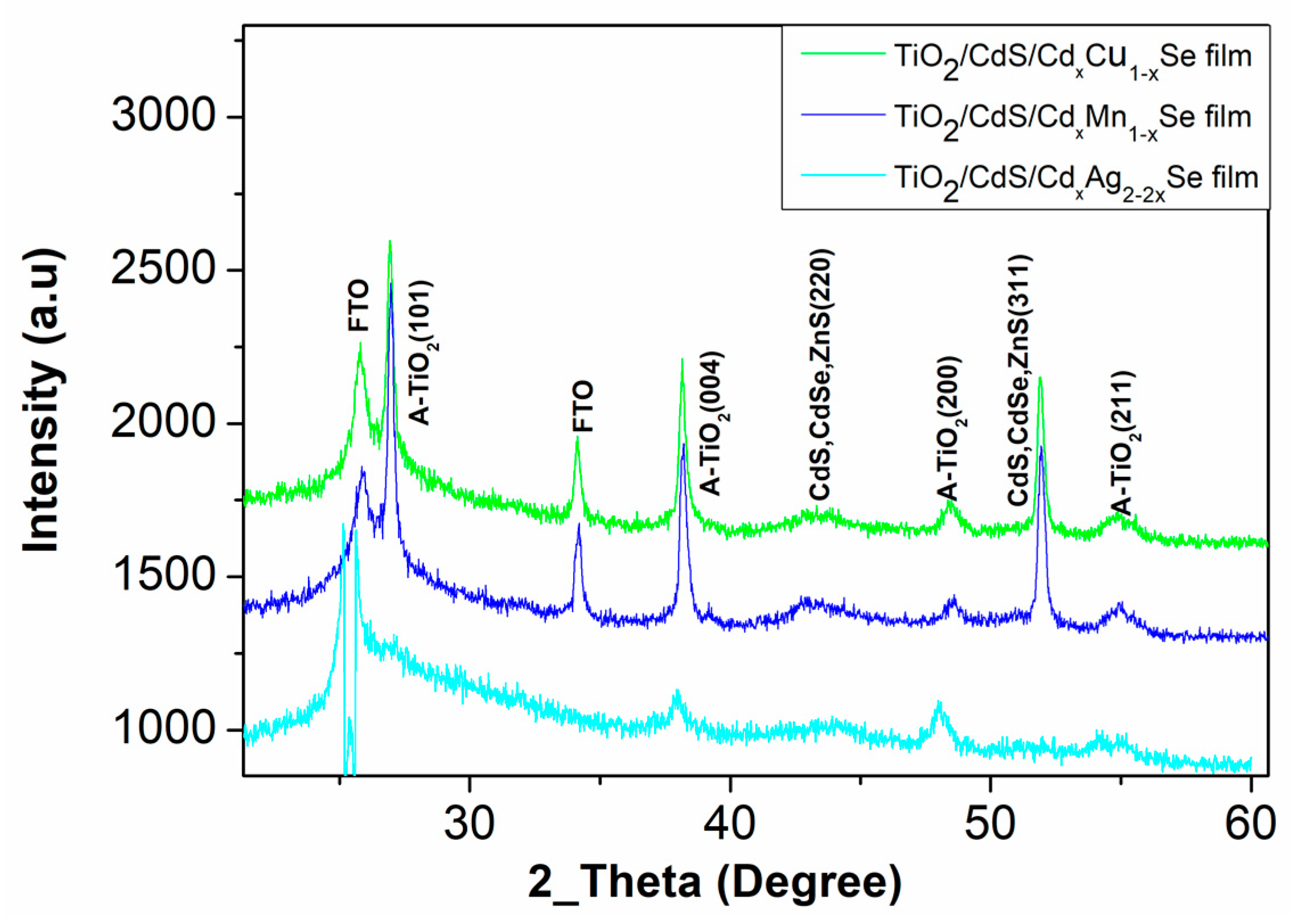
The structural TiO2/CdS/CdxCu1−xSe, TiO2/CdS/CdxMn1−xSe, and TiO2/CdS/CdxAg2−2xSe QDSSCs have been performed by X-ray diffraction. The obtained X-ray diffraction patterns are shown in Figure 1. For all thin films, the chart lists various parameters calculated from the diffraction peaks at 43.2° and 50.1° corresponding to the (220) and (311) crystal planes, respectively, of CdS, and CdSe zinc blende structure (JCPDS No. 88-2346 and JCPDS No. 41-1019) [12]. The peaks at 25.4°, 37.6°, 47.5° and 54.5° correspond to the (101), (004), (200), and (211) planes of the TiO2 Anatase structure [13]. In addition, the peak at 25 °C for TiO2/CdS/CdxCu1−xSe, TiO2/CdS/CdxMn1−xSe, and TiO2/CdS/CdxAg2−2xSe films conducted from the FTO, because all films were coated on the FTO [13].
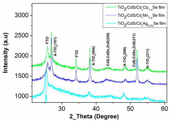
Figure 1.
The X-ray diffraction of the TiO2/CdS/CdxCu1−xSe, and TiO2/CdS/CdxMn1−xSe and TiO2/CdS/CdxAg2−2xSe QDSSCs.
2.2. Optical Characterization
In photovoltaic cells, both the optical and electrical features of component materials must be investigated extensively. In this study, the absorption spectra, transmission, and reflection spectra of QDSSCs were recorded using UV-Vis. From the absorption spectra, we can determine various optical parameters, such as the absorption coefficient, Eg of materials to control further band tail and study the defect states inside materials. TiO2/CdS/CdxCu1−xSe, TiO2/CdS/CdxMn1−xSe, and TiO2/CdS/CdxAg2−2xSe films recorded approximately 11.7 µm, 12.675 µm, and 13.013 µm of thickness from Figure 2, respectively.
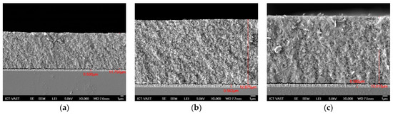
Figure 2.
The FE-SEM of (a) TiO2/CdS/CdxCu1−xSe, (b) TiO2/CdS/CdxMn1−xSe, and (c) TiO2/CdS/CdxAg2−2xSe films.
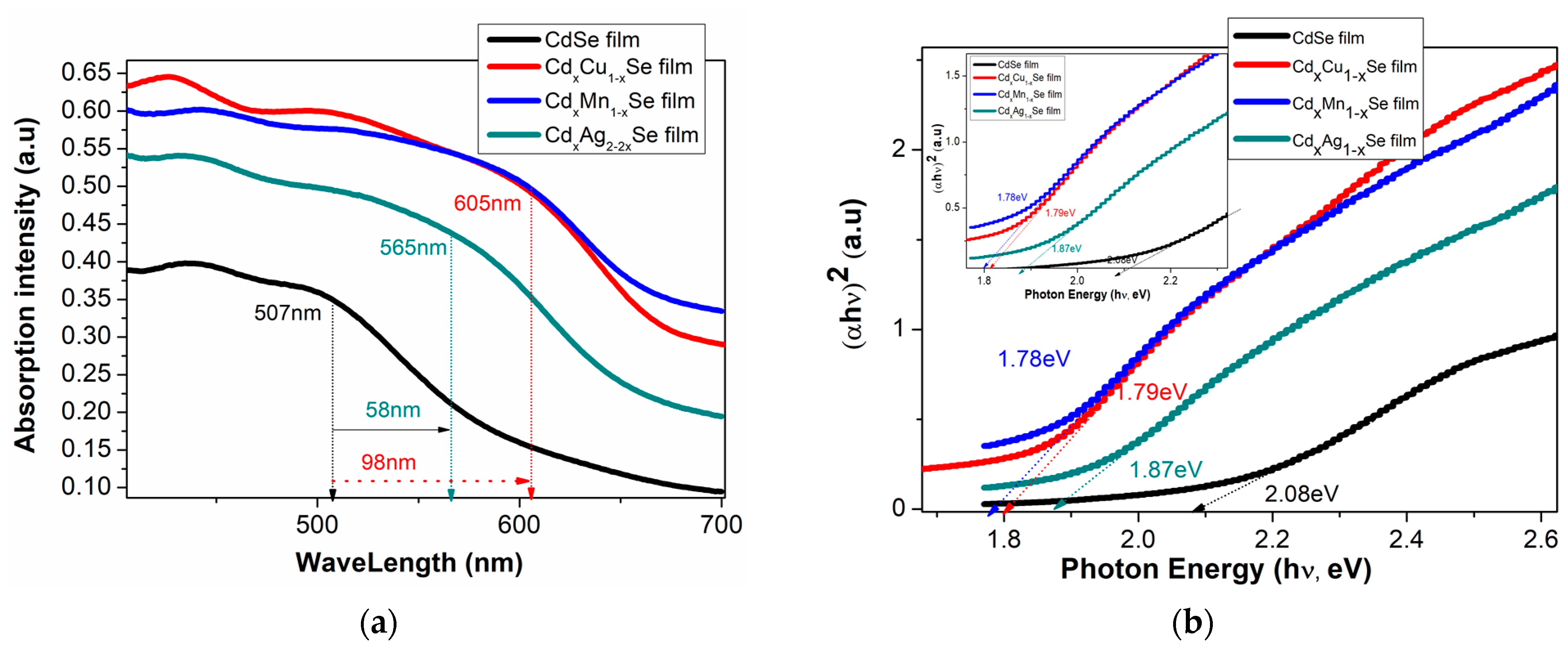
In Figure 3a, the absorbance density of the TiO2/CdS/CdxCu1−xSe, TiO2/CdS/CdxMn1−xSe, and TiO2/CdS/CdxAg2−2xSe thin films significantly increased by approximately 17%, when compared with undoped film with that of TiO2/CdS/CdxCu1−xSe photoanode. Moreover, the absorption density of the TiO2/CdS/CdxAg2−2xSe thin films decreased by approximately 11%, when compared with TiO2/CdS/CdxCu1−xSe thin films. Furthermore, the absorption density of TiO2/CdS/CdxCu1−xSe, TiO2/CdS/CdxMn1−xSe, and TiO2/CdS/CdxAg2−2xSe photoanodes shifted towards a longer wavelength (from 507 nm for undoped films to 605 nm for doped films). This is attributed to the replacement of the Cd atoms by the metal atoms in the films and a proper crystallization of the films corresponding to a suitable doping-concentration-reducing effect state [14]. The 605 nm absorption peak of the TiO2/CdS/CdxCu1−xSe film was attributed to the transition of the VB of Se to d-state of Cu dopant in the Eg of pure CdSe QDs [15].
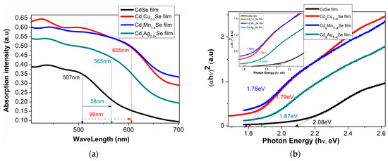
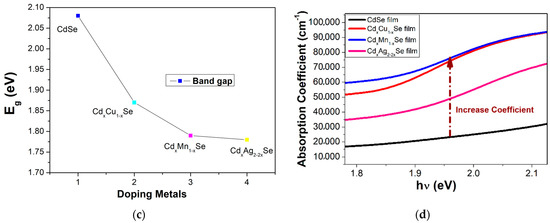
Figure 3.
Variation in (a) the absorption spectra and (b) (αhν)2 plots with the changing Ag ratio and the dependence of (c) Eg and (d) the absorption coefficient on the compositional TiO2/CdS/CdxCu1−xSe, and TiO2/CdS/CdxMn1−xSe, and TiO2/CdS/CdxAg2-2xSe thin films.
From the UV-Vis spectra, using the Tauc relation in Equation (1), we variously determined the Eg of the TiO2/CdS/CdxCu1−xSe, TiO2/CdS/CdxMn1−xSe, and TiO2/CdS/CdxAg2−2xSe films with dopants [16]
where α is noted as a coefficient of light coming adsorption, is noted as a light coming energy, αo is not the change factor, CdSe QDs has the direct band gap, and n = 0.5. After plotting Equation (1) in Figure 3b, Eg of the films was estimated and recorded (shown in Table 1).

Table 1.
Eg, CB, and VB were estimated by Tauc equation and the band tail, σ, Ee-p were obtained from the absorption spectra.
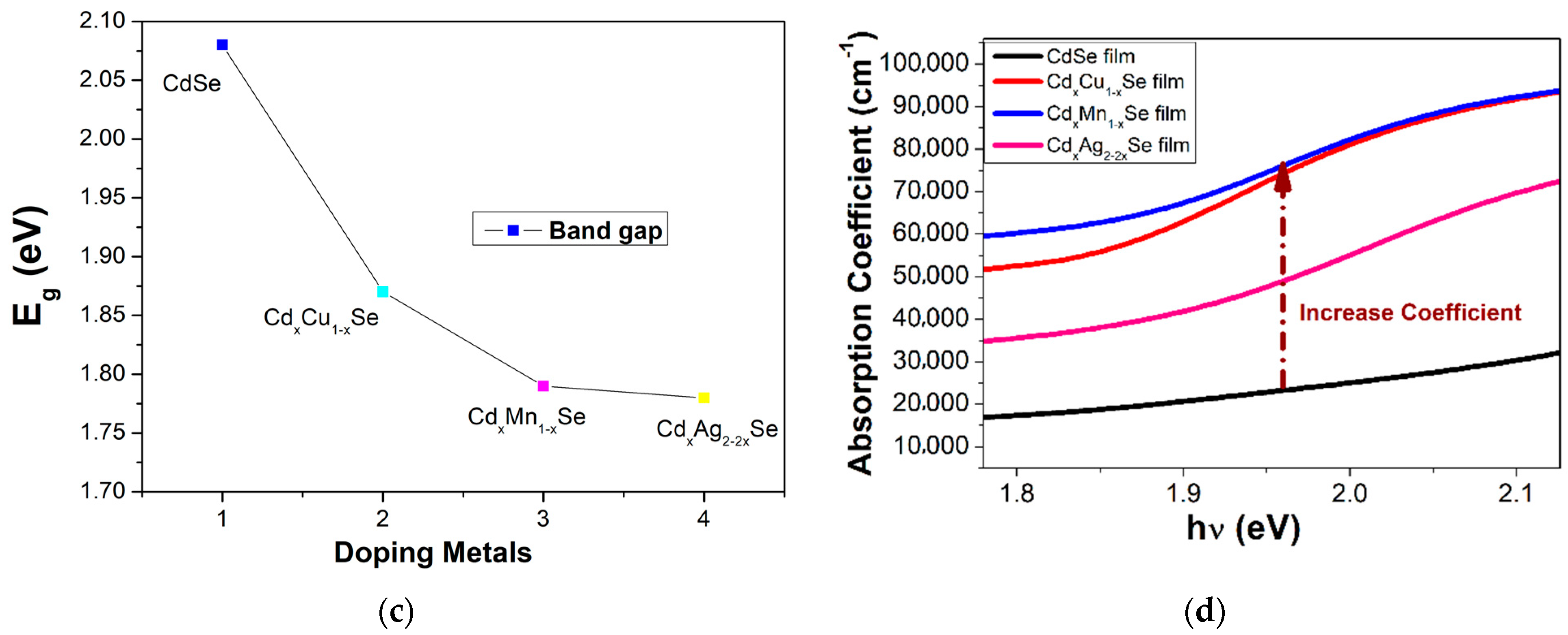
Figure 3b,c illustrates the valuable Eg for CdSe-doped photoanodes varying from 1.87 eV to 1.78 eV, which is smaller than that without doped photoanode (2.08 eV). Furthermore, by observation, the Eg values of CdSe-doped photoanodes depended significantly on the change in dopants. Here, the reduced Eg of the doped films resulted from two factors: an increase in particle size after doping [17], and a change in force density on account of the presence of Cu-Se, Mn-Se, and Ag-Se pairs in the extended lattice at the expense of Cd-Se in the host lattice [18]. Therefore, the dopant energy levels, called transition energies, are presented in the Eg of pure CdSe QDs. Subsequently, these photons obtain energy below Eg of pure CdSe nano semiconductor, which can be absorbed at dopant energy levels before they are transferred to the CB of pure CdSe semiconductor. Therefore, JSC was significantly increased on account of a large number of absorbed photons and, consequently, the absorption peak shifted towards to a longer wavelength. Furthermore, both the conduction band and valence band positions of the TiO2/CdS/CdxCu1−xSe, TiO2/CdS/CdxMn1−xSe, and TiO2/CdS/CdxAg2−2xSe films were estimated by the Tauc formula and listed in Table 1. Obtained CB values of −3.98, −3.7, and −4.1 eV corresponding to the TiO2/CdS/CdxCu1−xSe, TiO2/CdS/CdxMn1−xSe, and TiO2/CdS/CdxAg2−2xSe films, respectively, are higher than the CB value of −4.105 eV of pure CdSe QDs. Therefore, the presence of doping metals, which has increased the CB value in the doped films compared to that in the undoped CdSe QDs, aids in the transition of excited electrons from the CdSe QDs to TiO2.
Due to the band structure and transition energies of materials in the absorption process, the absorption coefficient is estimated using an equation correlation [19], as follows
where A and d are the absorption density and the thickness of the film, respectively.
As can be seen in Figure 3d, significantly increases after doping, and a shift in the absorption peak for CdSe doping metals compared to that without dopant occurs. This result, obtained from the replacement of Cd atoms by the metal dopants in the doped films, which induces the d-state electrons of dopant atoms, appeared in Eg of CdSe QDs to introduce the energy levels of dopant in the Eg of CdSe QDs. Therefore, the absorption coefficient of the doped films was enhanced significantly because the appearance of the transition energy levels ensured that a large number of photons was absorbed in different regions [20,21].
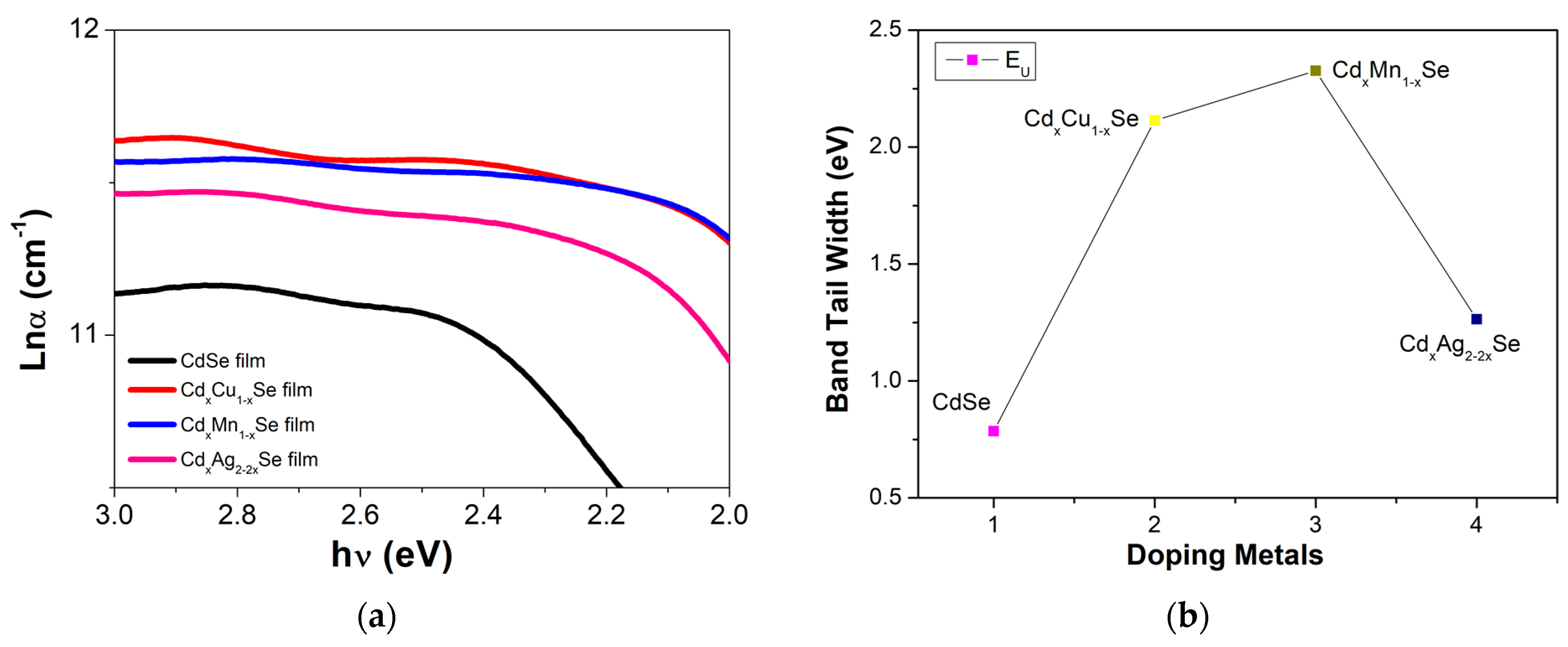
To correlate the localized states with the Eg of the films, the Urbach energy (Eu) of the films was determined as follows [22]
The Urbach plots between ln(α) and and Eu (which are estimated from the slope of the curves between ln(α) and ) are shown in Figure 4. As is evident, the valuable Eu depends on the type of doping metal. There was a minor decrease in its Eu, from 0.786 eV (undoped film) to 2.33 eV (doped films), due to the reduced defect states in the TiO2/CdS/CdxCu1−xSe, TiO2/CdS/CdxMn1−xSe, and TiO2/CdS/CdxAg2−2xSe films [23]. The Eu value of 2.33 eV was achieved for Cu doping, and was approximately two times higher than the band tail energy values for Mn and Ag doping (shown in Table 1). This implies that the large defect states in the films are a result of the unsatisfied bond, and the center of those defect states in Eg of the TiO2/CdS/CdxCu1−xSe, TiO2/CdS/CdxMn1−xSe, and TiO2/CdS/CdxAg2−2xSe films. Depending on the dopant, the defect state center can appear in the middle of Eg, near the VB, or near the CB [24].
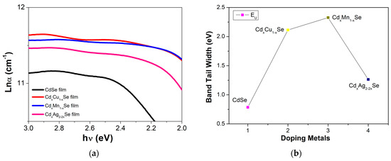
Figure 4.
The dependence of (a) the ln(α) of the films and (b) the Band tail energy on the compositional TiO2/CdS/CdxCu1−xSe, and TiO2/CdS/CdxMn1−xSe and TiO2/CdS/CdxAg2−2xSe thin films.
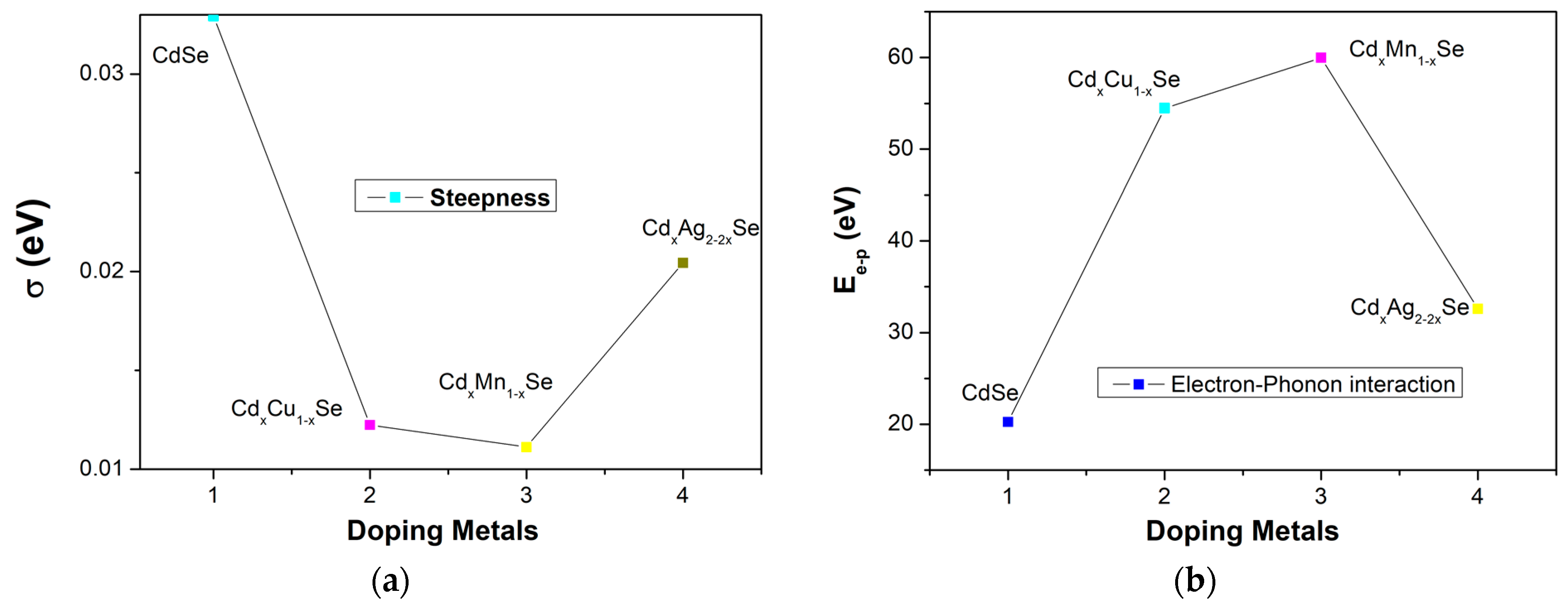
The absorption spectrum of the photovoltaic cells depends on several factors, such as the type of doping material, doping concentration, photoconductivity, thickness of the film, and especially, photon absorption in film. The steepness parameter, σ, is considered to result from the electron–phonon interaction (Ee-p). σ is correlated with Ee-p via the following correlation: Ee-p = 3/2σ. Figure 5 and Table 1 show the variations in σ and Ee-p, respectively. As can be seen in Figure 4a, σ shows a downward trend as the concentration of the doping metal reduced to a minimum of 3% (0.011 eV), which implies a stronger electron–phonon interaction energy corresponding to the TiO2/CdS/CdxCu1−xSe film as a result, confirming that the bond energy is as a parameter of film composition [24]. Furthermore, the Ee-p value for the TiO2/CdS/CdxCu1−xSe film (59.97 eV) is significantly higher than for the TiO2/CdS/CdxAg2−2xSe film (32.6 eV) or the CdSe film (20.25 eV), and σ increases considerably. Evidently, the compositional variations in ternary TiO2/CdS/CdxCu1−xSe, TiO2/CdS/CdxMn1−xSe, and TiO2/CdS/CdxAg2−2xSe thin films caused variations in the optical parameters [24].

Figure 5.
The dependence of (a) σ and (b) Ee-p in metal addition in films.
2.3. Electrical Properties
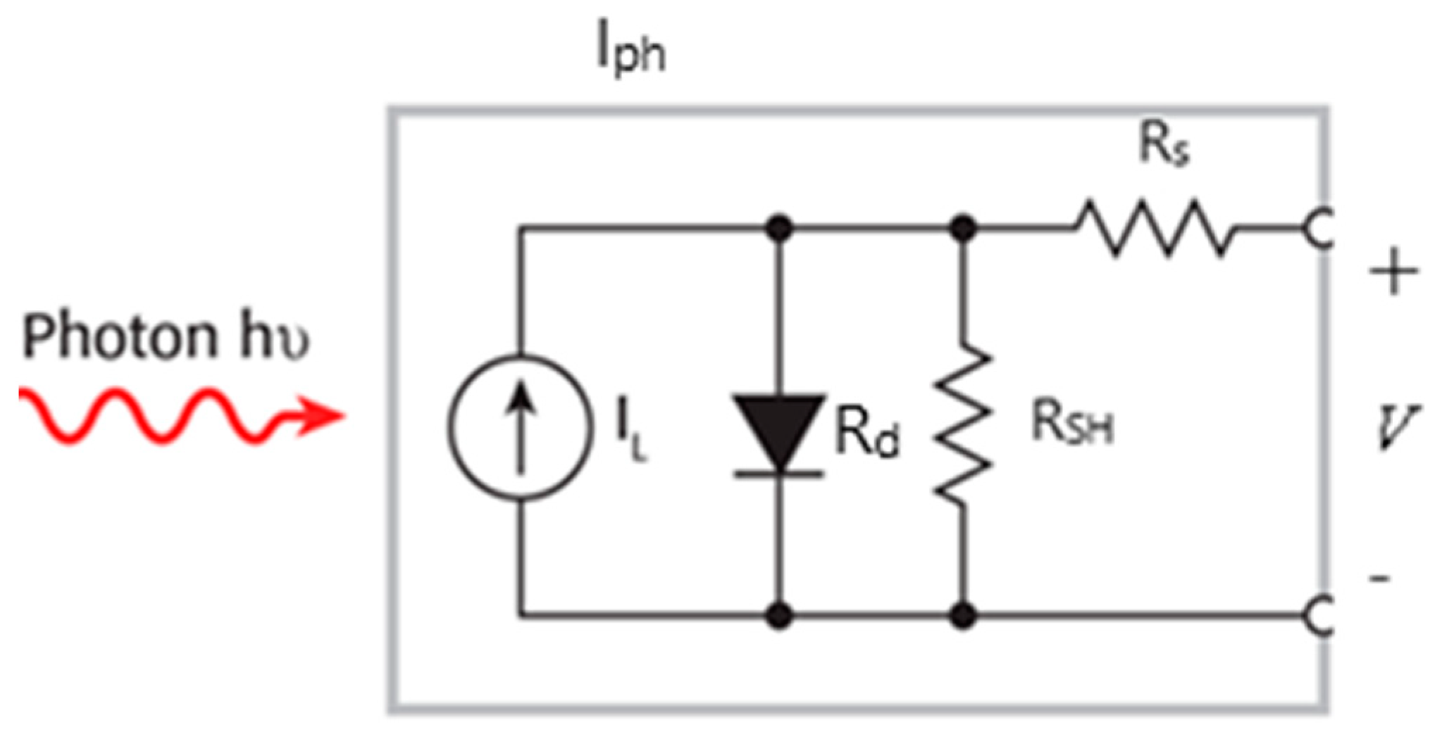
In this section, we study the current–voltage (J-V) characteristics of QDSSCs and, subsequently, the estimated primary physical parameters using one illuminated J-V curve. The photovoltaic device significantly depends on the four resistances in a photovoltaic cell: an external resistance (RD), internal resistance (Rd), series resistance (Rs), and a shunt resistance (RSH) (Figure 6). Ideally, Rs should be zero, and RSH should be infinite. As a result of the dynamic parameters, significant power losses caused by the dynamic resistances due to various factors, such as manufacturing defects, technological processes, and natural materials, are estimated.

Figure 6.
The circuit of a photovoltaic cell [25].
In [26], we conducted the equations for dynamic parameters as follows
where q and kB are the electronic charge and Boltzmann constant, respectively, T is the room temperature, Iph is the incident light intensity, and Io is the diode saturation current. The obtained physical parameters are listed in Table 2.
Table 2.
The values of the performance efficiency (efficiency, short-circuit current, open-circuit voltage, fill factor) and RD, Rd, RSH, Rs were estimated from J-V curves and Rct1, Rct2 were obtained from the EIS experiment.
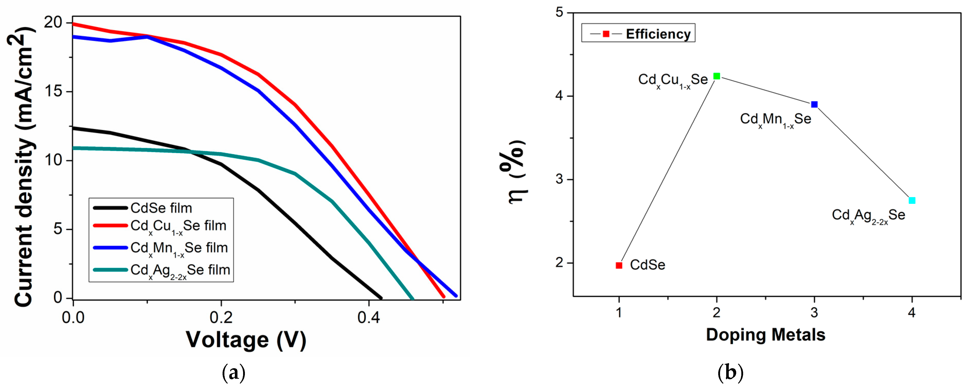
In this experiment, samples of photovoltaic cells fabricated using the TiO2/CdS/CdxCu1−xSe, TiO2/CdS/CdxMn1−xSe, and TiO2/CdS/CdxAg2−2xSe photoanodes were recorded by a Keithley 2400 source meter under identical illumination condition. Figure 7a,b show the graphical representation of the measurement results. The performance efficiency of the photovoltaic cells is sensitive to the concentration of the metal dopants (Figure 6). For example, the energy conversion value increased significantly from 1.97% (undoped film) to 4.24% (TiO2/CdS/CdxCu1−xSe film), and the highest efficiency was obtained for Cu doping. Furthermore, the efficiency dropped to 2.75% (for TiO2/CdS/CdxAg2−2xSe film). Furthermore, the valuation parameters of the photovoltaic cells were significantly influenced by doping metals; the corresponding experimental values are recorded in Table 2.
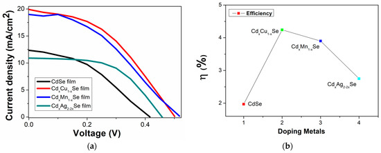
Figure 7.
(a) Variation of photocurrent density–voltage curves and (b) dependence of the performance efficiency on metal addition in films.
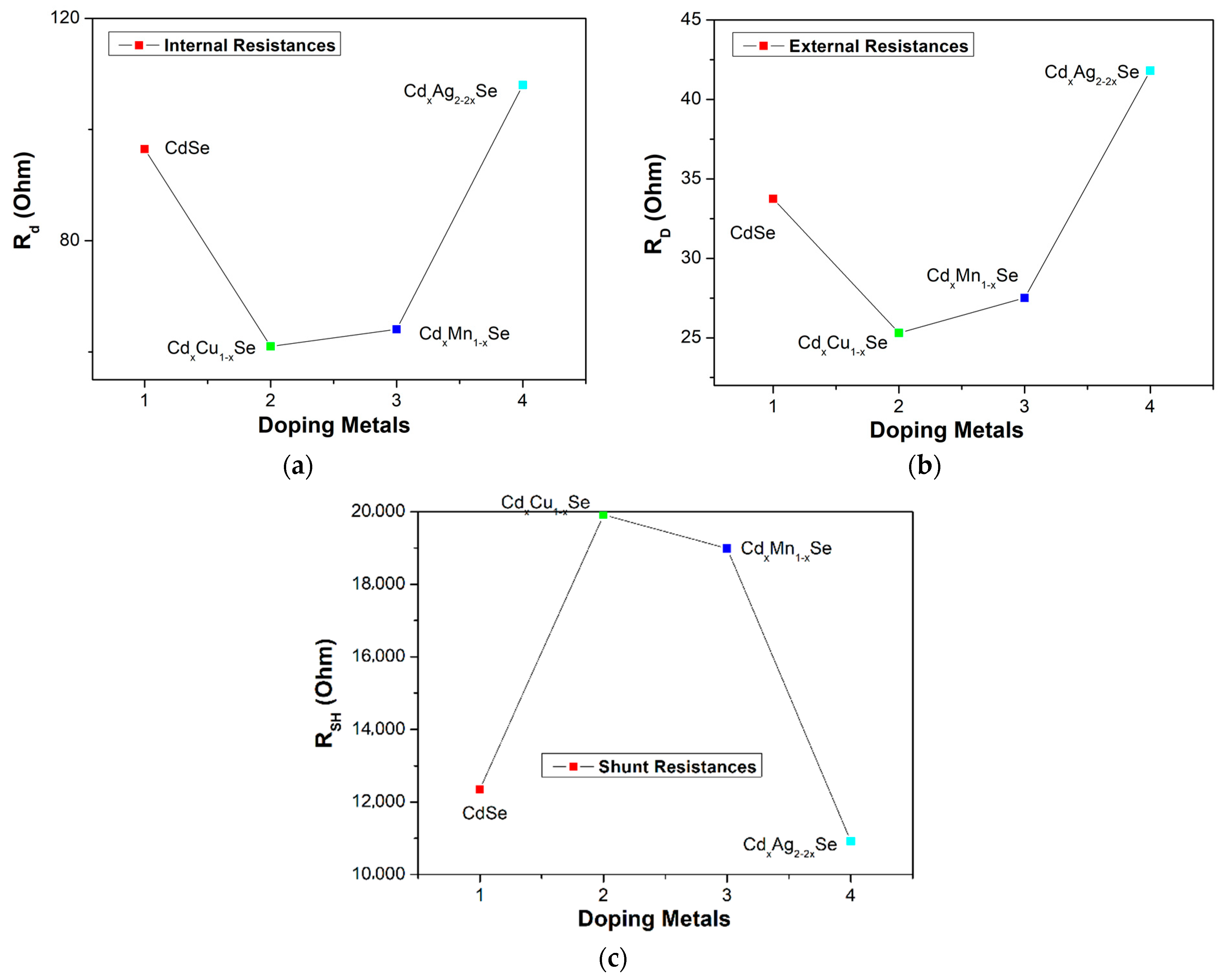
The values of the RD, Rd, and RSH of the photovoltaic cells are extracted from the photocurrent density curves in Figure 8a–c, and one J-V curve method, and listed in Table 2. Moreover, Rs is the resistance between the external circuit and the counter electrode photoanode. Generally, Rs drops rapidly with the doping of metal dopants because of the difference between RD and Rd value of Rs decreased from 62.8 Ω (undoped film) to 35.7 Ω (TiO2/CdS/CdxCu1−xSe film). Here, RD is the resultant of RSH, Rd (through the diode), and Rs. The value of RD was lowest for the TiO2/CdS/CdxCu1−xSe film, and increased to attain 66.2 Ω for the TiO2/CdS/CdxAg2−2xSe film. Generally, the value of RD of the doped films is lower than that of the undoped film because the replacement of the Cd atoms in the CdSe film hosted by the metal dopants reduced resistance inside each layer and at multilayer surfaces. Moreover, a leakage current generated in the technology process can change RD. Therefore, while RSH should be infinite for an ideal photovoltaic cell, practically, there is an upper limit of 20 kΩ for RSH. According to Table 2, the RSH values for doped films are higher without dopant, and the highest, 19.9 kΩ, is obtained from the TiO2/CdS/CdxCu1−xSe film. Evidently, RSH is sensitive to the doping metal; while, for C doping, RSH reaches a maximum value of 19.9 kΩ, for Ag doping, RSH value decreased to 10.92 kΩ for TiO2/CdS/CdxAg2−2xSe film. This result was also proven as the UV-Vis peak moves to a longer wavelength owing to the reduced Eg and enhanced Ee-p discussed in Section 3.2. Furthermore, our result also agrees with reference [26].
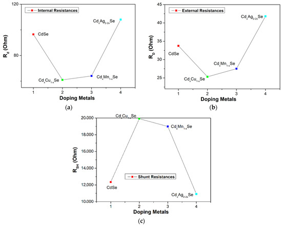
Figure 8.
Dependence of (a) the external resistance, (b) internal resistance, and (c) shunt resistance on metal addition in films.
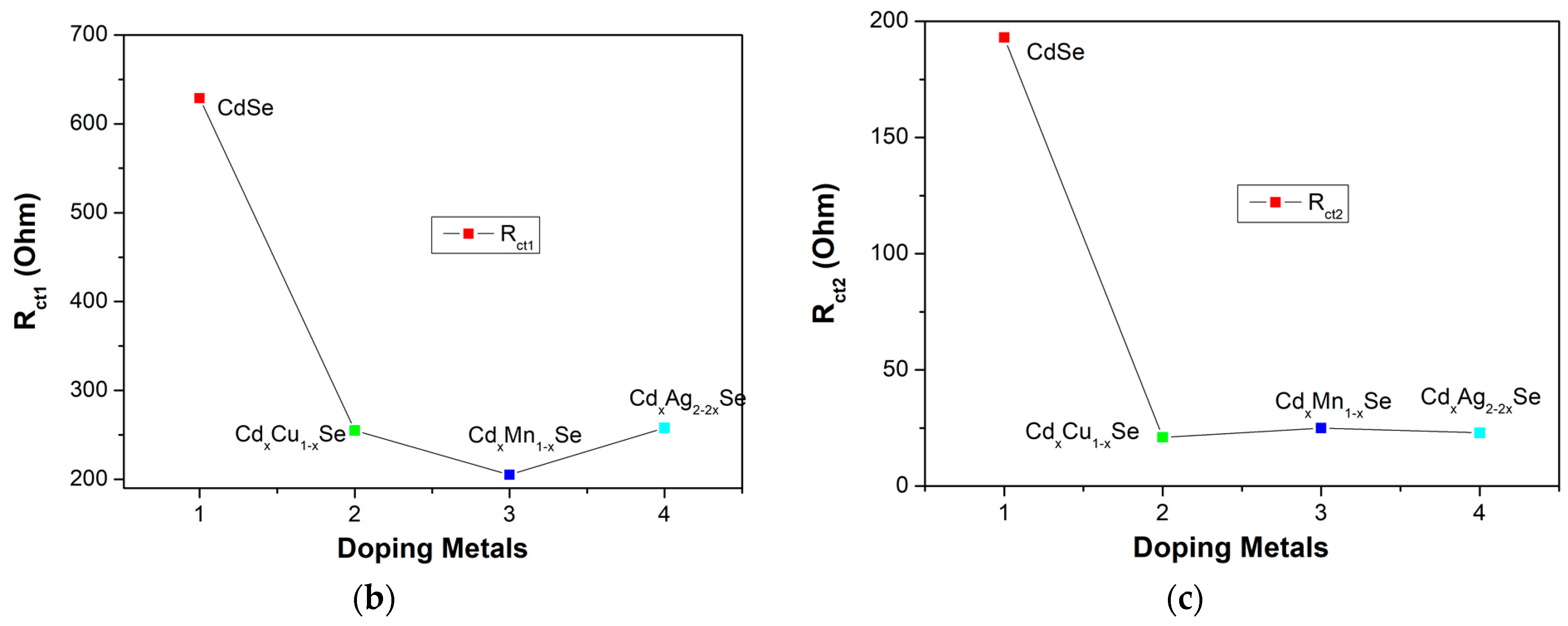
Conventionally, electrochemical impedance spectroscopy (EIS) was found by Mosa–Sero [27] to determine the occurring processes through contacts, TiO2 film and polysulfide electrolyte. These investigation and analysis processes included several steps, such as the pumping of excited charges from the CB of QDs to the CB of TiO2, diffusive charges inside the TiO2 film before moving to the external circuit, the transfer of electrons to the counter electrode/polysulfide. In this case, an equivalent circuit was extracted from the EIS fitting using the Nova software. As far as the EIS fitting is concerned, the equivalent circuits for simulation were chosen for a consistent match between the EIS experiment and EIS fitting. Subsequently, Rct1 and Rct2 were obtained from EIS fitting. Those values are listed in Table 2.
Figure 9a–c shows the EIS curves of the photovoltaic cells based on the metal dopants, and dynamic resistance curves in the counter electrode/polysulfide electrolyte surface, and in the redox process of electrolysis, Rct1, and the recombination resistance at TiO2/QDs surface, and in TiO2 film, Rct2. In the same way, the recombination resistances, which are listed in Table 2, depend significantly on the doping concentration of the metal dopants. A downward trend was observed Rct1 value from 629 Ω (undoped film) to 205 Ω (TiO2/CdS/CdxMn1−xSe film) or to 255 Ω (TiO2/CdS/CdxCu1−xSe film). The value of Rct1 was the lowest (205 Ω) for the TiO2/CdS/CdxMn1−xSe film, and it increased to a maximum value of 256Ω for the TiO2/CdS/CdxAg2-2xSe film. This implies that a decrease in the recombination resistance at the counter electrode/polysulfide electrolyte surface and in the redox process of the electrolyte resulted in the enhanced current density (19.89 mA/cm2) and energy conversion (4.24%) compared to those for the undoped film (12.4 mA/cm2 and 1.97%, respectively) [28]. Furthermore, as mentioned above, the correlation with Rct2 caused the recombination resistance in the photovoltaic cells, which indicates that the recombination processes at TiO2/QDs surface, inside QDs, and the diffusion of charges in TiO2 film were correlated to the TiO2/CdS/CdxCu1−xSe film, TiO2/CdS/CdxMn1−xSe film, and TiO2/CdS/CdxAg2-2xSe film. Therefore, Rct2 is pivotal in explaining the enhanced current density and performance efficiency after the proposed metal doping. Correspondingly, the values of the Rct2 decreased from 193 Ω (undoped film) to 21 Ω (Cu doping). The value of Rct2 was the lowest for Cu doping (21Ω), and increased to a maximum of 23 Ω for Ag doping. This result is consistent with the results from the photocurrent density curve, absorption spectra, and the band tail energy. Because of the reduced recombination resistance, a large number of charges accumulated, further reducing the recombination process of the excited electrons with the surface states of QDs, resulting in the fast pumping of excited charges between CdS, CdSe and TiO2 [29].
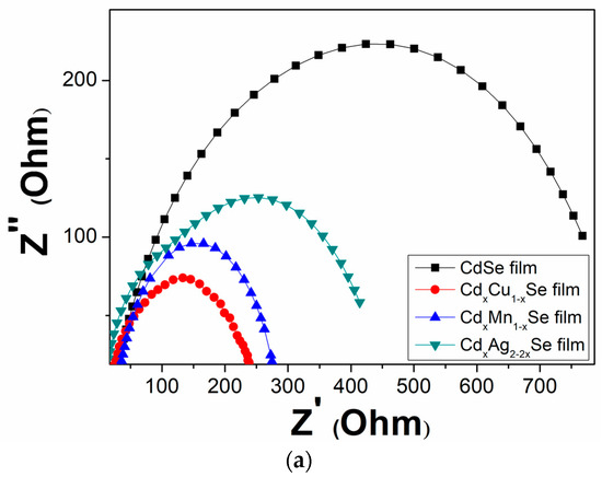
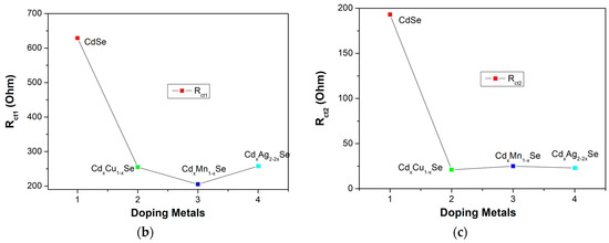
Figure 9.
(a) Variation of the Electrochemical Impedance Spectra and (b) dependence of the recombination resistances: (b) polyelectrolyte and polyelectrolyte/counter electrode contact (Rct1) and (c) TiO2/QDs contact and diffusion resistance in TiO2 films (Rct2).
3. Experiment
3.1. Materials
TEC7 Glass Plates 3.2 mm (2.2 mm of thickness, 1.2 × 2 cm = 0.196 cm2 of area) was purchased from Sigma in Frankfurter, German. Titania paste, Sodium Selenite (Na2SeO3), Cd(NO3)2. 2H2O, Na2S.9H2O, Cu(NO3)2. 3H2O, Mn(CH3COO)2.4H2O, AgNO3, Na2SO3, NaOH, Se powder, KCl, Na2S, S were bought from Sigma in Frankfurter, German. All chemicals were used directly without further purification.
3.2. Preparation Processes
TiO2 film was coated on the Fluorine-doped tin oxide (FTO) followed by annealing in air at 500 °C.
Fabrication of CdS film: The FTO/TiO2 film was dipped in Cd2+-solution (2.665 g Cd(NO3)2.2H2O dissolved in a 20 mL mixture of ethanol and pure water in 1:1 ratio) for 5 min, and then washed with ethanol. Furthermore, it was dipped in S2− solution (12 g of Na2S.9H2O, dissolved in 100 mL mixture of methanol and pure water in 1:1 ratio) for 5 min and then washed with methanol. This two-step process formed a single layer of the CdS film. Two layers of the CdS film were coated by repeating the two-step process.
Fabrication of Cu2+ Doped, Mn2+ Doped, and Ag+ Doped CdSe Films
For Cu2+ doping, Cd2+ and Cu2+-solution (0.1 M Cd(NO3)2.2H2O and 0.1 M Cu(NO3)2.3H2O dissolved in a 30 mL mixture of ethanol and pure water in 1:1 ratio) was kept for 5 min, and then washed with ethanol.
For Mn2+ doping, Cd2+ and Mn2+-solution (0.1 M Cd(NO3)2. 2H2O and 0.1 M Mn(CH3COO)2. 4H2O dissolved in 30 mL mixture of methanol and pure water in 1:1 ratio) was kept for 5 min, and then washed with methanol.
For Ag+ doping, Cd2+ and Ag+-solution (0.1 M Cd(NO3)2. 2H2O and 0.1 M AgNO3 dissolved in a 30 mL mixture of ethanol and pure water in 1:1 ratio) was kept for 5 min, and then washed with ethanol.
Furthermore, for the fabrication of Cu2+, Mn2+, and Ag+ doped films, the previously synthesized FTO/TiO2/CdS were, respectively, separately dipped into the solutions mentioned above. Subsequently, the films were dipped in Se2−-solution (2.27 g Se powder and 0.6 M Na2SO3 were dissolved in 100 mL of water and then added to 5 mL of 1 M NaOH. Furthermore, the solution was stored at 70 °C in 7 h) for 15 min at 50 °C, and then washed with pure water to form a single layer of the CdSe film desired doping material. Three layers of the CdSe film with the desired doping material were coated by repeating the above process. Finally, the films were annealed in the range from 120 °C to 300 °C as in vacuum for 30 min.
The polysulfide electrolyte was prepared by mixing 0.5 M Na2S, 0.2 M S, and 0.2 M KCl in pure water in 7:3 ratio.
The photoanodes have been synthesized and characterized using XRD (Philips, PANalytical X’Pert, CuKα radiation). The absorption spectra were recorded using a UV-Vis JASCO V-670. The completed photovoltaic cells were characterized using a Keithley 2400 source meter developed by SOLARENA, Sweden. The obtained J-V curves are supported to estimate the valuable electrical range of devices. The scanning speed voltage of the equipment was set at 5 mV/s in the range from VOC to 0. The electrochemical impedance spectroscopy was performed using an impedance analyzer (ZAHNER CIMPS).
4. Conclusions
TiO2/CdS/CdxCu1−xSe, TiO2/CdS/CdxMn1−xSe, and TiO2/CdS/CdxAg2-2xSe thin films were successfully synthesized on FTO glass as photoanodes in solar cells, which were sensitive to Cu2S counter electrode. The QDSSCs using the TiO2/CdS/CdxCu1−xSe photoanode exhibits the highest performance: JSC = 19.89 mA/cm2, VOC = 0.505 V, FF = 0.379, and η = 4.24% as a result of enhancing electrocatalytic activity, charge transfer and charge collection, reducing recombination, and the longer excited electron lifetime. The optical parameters also are sensitive to dopant. This implies that large defect states in the films are a result of the unsatisfied bond and the center of those defect states in Eg of CdxCu1−xSe films. They can be seen in the middle of Eg, near the VB, or near the CB. Furthermore, the electrical properties of the CdxCu1−xSe were also investigated through the Rs, RSH dynamic resistance, recombination resistance, diffusion resistance in TiO2 layer, and TiO2/QDs, Rct1, Rct2. As a result, the recombination and dynamic resistance of TiO2/QDs and diffusion in TiO2 (Rct2) films, and the diffusion at the counter electrode/electrolyte (Rct1), decreased significantly.
Author Contributions
Conceptualization, D.H.P. and H.T.T.; methodology, D.H.P. and H.T.T.; formal analysis, D.H.P., H.T.T., V.-C.N. and M.H.N.T.; in-vestigation, D.H.P. and H.T.T.; data curation, D.H.P. and H.T.T.; writing—original draft preparation, D.H.P. and H.T.T.; writing—review and editing, D.H.P., H.T.T., V.-C.N. and M.H.N.T.; funding acquisition, D.H.P. and H.T.T. All authors have read and agreed to the published version of the manuscript.
Funding
This research is supported by Industrial University of Ho Chi Minh City (IUH) under grant number 112/HD-DHCN.
Institutional Review Board Statement
Not applicable.
Informed Consent Statement
Not applicable.
Data Availability Statement
The data presented in this study are available on request from the corresponding author.
Conflicts of Interest
The authors declare no competing interests.
References
- Chattopadhyay, S.; Sen, P.; Andrews, J.T.; Sen, P.K. Semiconductor core-shell quantum dot: A low temperature nano-sensor material. J. Appl. Phys. 2012, 111, 034310. [Google Scholar] [CrossRef]
- Ariful, A.; He, T.; Eid, K.; Abdullah, A.M.; Curry, M.L.; Du, A.; Puente Santiago, A.R.; Echegoyen, L.; Noveron, J.C. Tuning the Intermolecular Electron Transfer of Low-Dimensional and Metal-Free BCN/C60 Electrocatalysts via Interfacial Defects for Efficient Hydrogen and Oxygen Electrochemistry. J. Am. Chem. Soc. 2021, 143, 1203–1215. [Google Scholar]
- Sanchez-Ramirez, E.A.; Hernandez-Perez, M.A.; Aguilar-Hernandez, J.; Rangel-Salinas, E. Nanocrystalline CdS1−xSex alloys as thin films prepared by chemical bath deposition: Effect of x on the structural and optical properties. J. Alloys Compd. 2014, 615, 511–514. [Google Scholar] [CrossRef]
- Husain, M.; Pal Singh, B.; Kumar, S.; Sharma, T.P.; Sebastian, P.J. Optical, electrical and structural investigations on Cd1−xZnxSe sintered films for photovoltaic applications. Sol. Energy Mater. Sol. Cells 2003, 76, 399–415. [Google Scholar] [CrossRef]
- Sanchez-Ramirez, E.A.; Hernandez-Perez, M.A.; Aguilar-Hernandez, J.R. Study on the introduction of Se into CdS thin films: Influence on the kinetics of the deposition and the structural and optical properties. Appl. Surf. Sci. 2015, 347, 35–39. [Google Scholar] [CrossRef]
- Shockley, W.; Queisser, H.J. Detailed balance limit of efficiency of p-n junction solar cells. J. Appl. Phys. 1961, 32, 510–519. [Google Scholar] [CrossRef]
- Hagfeldt, A.; Boschloo, G.; Sun, L.; Kloo, L.; Pettersson, H. Dye-sensitized solar cells. Chem. Rev. 2010, 110, 6595–6663. [Google Scholar] [CrossRef] [PubMed]
- Phuc, D.H.; Tung, H.T. Band tunable CdSe quantum dot-doped metals for quantum dot-sensitized solar cell application. Int. J. Photoenergy 2019, 2019, 9812719. [Google Scholar] [CrossRef]
- Wang, P.; Abrusci, A.; Wong, H.M.P.; Svensson, M.; Anderson, M.R.; Greenham, N.C. Photoinduced charge transfer and efficient solar energy conversion in a blend of a red polyfluorene copolymer with CdSe nanoparticles. Nano Lett. 2006, 6, 1789–1793. [Google Scholar] [CrossRef]
- Fan, S.-Q.; Fang, B.; Kim, J.H.; Jeong, B.; Kim, C.; Yu, J.-S.; Ko, J. Ordered multimodal porous carbon as highly efficient counter electrodes in dye-sensitized and quantum-dot solar cells. Langmuir 2010, 26, 13644–13649. [Google Scholar] [CrossRef] [PubMed]
- Fan, S.-Q.; Cao, R.-J.; Xi, Y.-X.; Gao, M.; Wang, M.-D.; Kim, D.-H.; Kim, C.-W.; Ko, J.-J. CdSe quantum dots as co-sensitizers of organic dyes in solar cells for red-shifted light harvesting. Optoelectron. Adv. Mater. Rapid Commun. 2009, 3, 1027–1033. [Google Scholar]
- Song, L.; Duan, J.; Zhan, J. One-pot Microwave Assisted Synthesis of Homogeneously Alloyed CdSexTe1−x Nanocrystals with Tunable Photoluminescence. Mater. Lett. 2010, 64, 1843–1845. [Google Scholar] [CrossRef]
- Vogel, R.; Pohl, K.; Weller, H. Sensitization of highly porous, polycrystalline TiO2 electrodes by quantum sized CdS. Chem. Phys. Lett. 1990, 174, 241–246. [Google Scholar] [CrossRef]
- Tung, H.T.; Phuc, D.H.; Chung, N.T.K.; Thuy, N.T.N. Enhanced light absorption and charge recombination control in quantum dot sensitized solar cells using Copper and Manganese doped cadmium sulfide quantum dots. Environ. Prog. Sustain. Energy 2021, e13650. [Google Scholar] [CrossRef]
- Ramasamy, K.; Malik, M.A.; Helliwell, M.; Raftery, J.; O’Brien, P. Thio-and dithio-biuret precursors for zinc sulfide, cadmium sulfide, and zinc cadmium sulfide thin films. Chem. Mater. 2011, 23, 1471–1481. [Google Scholar] [CrossRef]
- Tauc, J.; Radu, G.; Anina, V. Optical properties and electronic structure of amorphous germanium. Phys. Status Solidi 1966, 15, 627–637. [Google Scholar] [CrossRef]
- Ha, T.T.; Chi, C.H.; Vy, N.T.; Thoa, N.T.P.; Huynh, T.D.; Lam, Q.V. Improving the performance of QDSSCs based on TiO2/CdS(Silar)/CdSe(Colloid)/Zns(Silar) photoanodes. Environ. Prog. Sustain. Energy 2015, 34, 1774–1779. [Google Scholar] [CrossRef]
- Ueda, Y.; Ohtani, T. Mechanochemical Synthesis, Vacancy-Ordered Structures and Low-Dimensional Properties of Transition Metal Chalcogenides. Handb. Solid State Chem. 2017, 383–433. [Google Scholar] [CrossRef]
- Al-Bataineh, Q.M.; Alsaad, A.M.; Ahmad, A.A.; Al-Sawalmih, A. Structural, electronic and optical characterization of ZnO thin film-seeded platforms for ZnO nanostructures: Sol–gel method versus ab initio calculations. J. Electron. Mater. 2019, 48, 5028–5038. [Google Scholar] [CrossRef]
- Siddiqui, F.Y.; Shaikh, S.U.; Desale, D.J.; Upadhye, D.S.; Mahajan, S.V.; Ghule, A.V.; Varshney, P.; Han, S.-H.; Sharma, R. Band gap engineering by substitution of S by Se in nanostructured CdS1− xSex thin films grown by soft chemical route for photosensor application. Mater. Sci. Semicond. Process. 2014, 27, 404–411. [Google Scholar] [CrossRef]
- Mondal, R.; Miyaki, N.; Becerril, H.A.; Norton, J.E.; Parmer, J.; Mayer, A.C.; Tang, M.L.; Brédas, J.-L.; McGehee, M.D.; Bao, Z. Synthesis of acenaphthyl and phenanthrene based fused-aromatic thienopyrazine co-polymers for photovoltaic and thin film transistor applications. Chem. Mater. 2009, 21, 3618–3628. [Google Scholar] [CrossRef]
- Urbach, F. The long-wavelength edge of photographic sensitivity and of the electronic absorption of solids. Phys. Rev. 1953, 92, 1324. [Google Scholar] [CrossRef]
- Venables, J. Introduction to Surface and Thin Film Processes; Cambridge University Press: Cambridge, UK, 2000. [Google Scholar]
- Pattanaik, A.K.; Srinivasan, A. Electrical and optical studies on Pb-modified amorphous Ge–Se–Te films. Semicond. Sci. Technol. 2003, 19, 157. [Google Scholar] [CrossRef]
- Neamen, D.A. Semiconductor Physics and Devices: Basic Principles; McGraw-Hill: New York, NY, USA, 2012. [Google Scholar]
- Muthalif, M.P.A.; Lee, Y.-S. Chozhidakath Damodharan Sunesh, Hee-Je Kim, and Youngson Choe. Enhanced photovoltaic performance of quantum dot-sensitized solar cells with a progressive reduction of recombination using Cu-doped CdS quantum dots. Appl. Surf. Sci. 2017, 396, 582–589. [Google Scholar] [CrossRef]
- Guijarro, N.; Lana-Villarreal, T.; Mora-Seró, I.; Bisquert, J.; Gómez, R. CdSe quantum dot-sensitized TiO2 electrodes: Effect of quantum dot coverage and mode of attachment. J. Phys. Chem. C 2009, 113, 4208–4214. [Google Scholar] [CrossRef]
- Shen, Q.; Kobayashi, J.; Diguna, L.J.; Toyoda, T. Effect of ZnS coating on the photovoltaic properties of CdSe quantum dot-sensitized solar cells. J. Appl. Phys. 2008, 103, 084304. [Google Scholar] [CrossRef]
- Rühle, S.; Shalom, M.; Zaban, A. Quantum-dot-sensitized solar cells. ChemPhysChem 2010, 11, 2290–2304. [Google Scholar] [CrossRef]


Publisher’s Note: MDPI stays neutral with regard to jurisdictional claims in published maps and institutional affiliations. |
© 2021 by the authors. Licensee MDPI, Basel, Switzerland. This article is an open access article distributed under the terms and conditions of the Creative Commons Attribution (CC BY) license (https://creativecommons.org/licenses/by/4.0/).