Article

Effect of 3d Transition Metal Atom Intercalation Concentration on the Electronic and Magnetic Properties of Graphene/MoS2 Heterostructure: A First-Principles Study

1
Department of Physics, Yancheng Institute of Technology, Yancheng 224051, China
2
College of Physics Science and Technology & Microelectronics Industry Research Institute, Yangzhou University, Yangzhou 225002, China
*
Author to whom correspondence should be addressed.
Molecules 2023, 28(2), 509; https://doi.org/10.3390/molecules28020509
Submission received: 2 December 2022 / Revised: 31 December 2022 / Accepted: 1 January 2023 / Published: 4 January 2023
(This article belongs to the Special Issue Recent Advance in Transition Metal Complexes and Their Applications)

Abstract

:
The electronic and magnetic properties of graphene/MoS2 heterostructures intercalated with 3d transition metal (TM) atoms at different concentrations have been systematically investigated by first principles calculations. The results showed that all the studied systems are thermodynamically stable with large binding energies of about 3.72 eV–6.86 eV. Interestingly, all the TM-intercalated graphene/MoS2 heterostructures are ferromagnetic and their total magnetic moments increase with TM concentration. Furthermore, TM concentration-dependent spin polarization is obtained for the graphene layer and MoS2 layer due to the charge transfer between TM atoms and the layers. A significant band gap is opened for graphene in these TM-intercalated graphene/MoS2 heterostructures (around 0.094 eV–0.37 eV). With the TM concentration increasing, the band gap of graphene is reduced due to the enhanced spin polarization of graphene. Our study suggests a research direction for the manipulation of the properties of 2D materials through control of the intercalation concentration of TM atoms.

1. Introduction

In the past decades, atomic layer-thick two-dimensional (2D) materials have been attracting tremendous attention due to their extraordinary properties and possible application in diverse fields. On the other hand, the inherent shortcomings of 2D materials in certain areas greatly limit their application in certain fields. As a star material, graphene (G) has been found to have high electron mobility, thermal conductivity, light transmission, and much more [1]; however, the lack of bandgap and magnetism largely limits graphene’s application in nanoelectronics. In addition to graphene, 2D transition metal dichloride (TMD) also appears to have attractive properties for various applications, such as use in the fabrication of optoelectronics, transistors, etc. [2]. For example, MoS2 is a direct bandgap semiconductor with a very high switching rate, but its electron mobility is as low as 200 cm−2 V−1 s−1, which greatly hinders its use in the development of electronic devices [3]. Phosphorene is found to have a moderate direct band gap and relatively high hole mobility [4]; nevertheless, it is very susceptible to the environment and degrades over time, which greatly hinders its widespread use in electronic and optoelectronic devices [5].
As one solution, the construction of 2D van der Waals (vdW) heterostructures by stacking different monolayers provides an efficient way of achieving more intriguing properties for a wide range of applications. Taking graphene as an example, the band gap can be opened when it is adsorbed on other 2D materials, such as MoS2 [6], h-BN [7], and borophene [8]. In G/WS2 heterostructures, the weak spin–orbit coupling of graphene can be enhanced by the proximity effect of WS2 [9]. When stacked with h-BN, graphene displays significantly enhanced electron mobility, which allows the fractional quantum Hall effect of graphene to be observed [10]. Despite this, there is still much room for improvement in the properties of graphene. For example, the opened band gap of graphene in the above heterostructures is too small to meet the requirements of electronic device application. Moreover, the heterostructure will not have magnetism once the heterogeneous monolayers are no longer magnetic.
To date, various approaches have been developed to further manipulate the properties of 2D vdW heterostructures, such as creating point defects [11,12], doping impurity atoms [13,14], applying electric fields [15], exerting external strains [16,17], and intercalating metal atoms [18,19]. Among them, the intercalation of metal atoms in the interlayer gap has become a promising way of designing the physical properties of 2D vdW heterostructures [20,21,22,23], which has the advantage of not disrupting the structure of the monolayer [24]. These intercalators can act as bridges between the monolayers separated by vdW gaps, effectively enhancing interlayer interactions and influencing material properties through charge transfer, band gap engineering, phonon scattering, and so on [25,26,27,28]. For example, Ca intercalation in bilayer graphene has been shown to induce superconductivity, which is not present in intrinsic graphite [29]. Furthermore, Li intercalation has been shown to tune conductivity in several layers of MoS2 [30] and graphene/MoX2 (X = S, Se) [31] heterostructures by more than two to three orders of magnitude. Furthermore, a 3d transition metal (TM) atom-intercalated bilayer graphene [32,33], bilayer borophene [34], G/MoS2 [35], G/WS2 [35], G/WSe2 [36], and defective G/WSe2 [36] were found to introduce new electronic and magnetic properties. It is noted that the properties of intercalation compounds should be closely related to the concentration of the intercalated atoms, which is easy to control in experiments [20]. Nevertheless, the influence of intercalation concentration on 2D vdW material properties is still unclear.
Taking the nonmagnetic G/MoS2 heterostructure as an example, we intercalated magnetic 3d TM atoms at different concentrations into the graphene and MoS2 interlayer gap and attempted to tune the electronic and magnetic properties of it. Our results show that all the studied systems were thermodynamically stable with large binding energies of about 3.72 eV–6.86 eV. With increases in TM concentration, the binding energies were decreased to some extent. Due to the spin polarization of 3d TM atoms, all the studied systems were found to be ferromagnetic. Furthermore, the graphene layer and MoS2 layer were spin-polarized because of the charge transfer between the TM atoms and the layer. Moreover, a significant band gap was opened in graphene, which decreased with the TM concentration increase owing to the enhanced spin polarization of graphene.

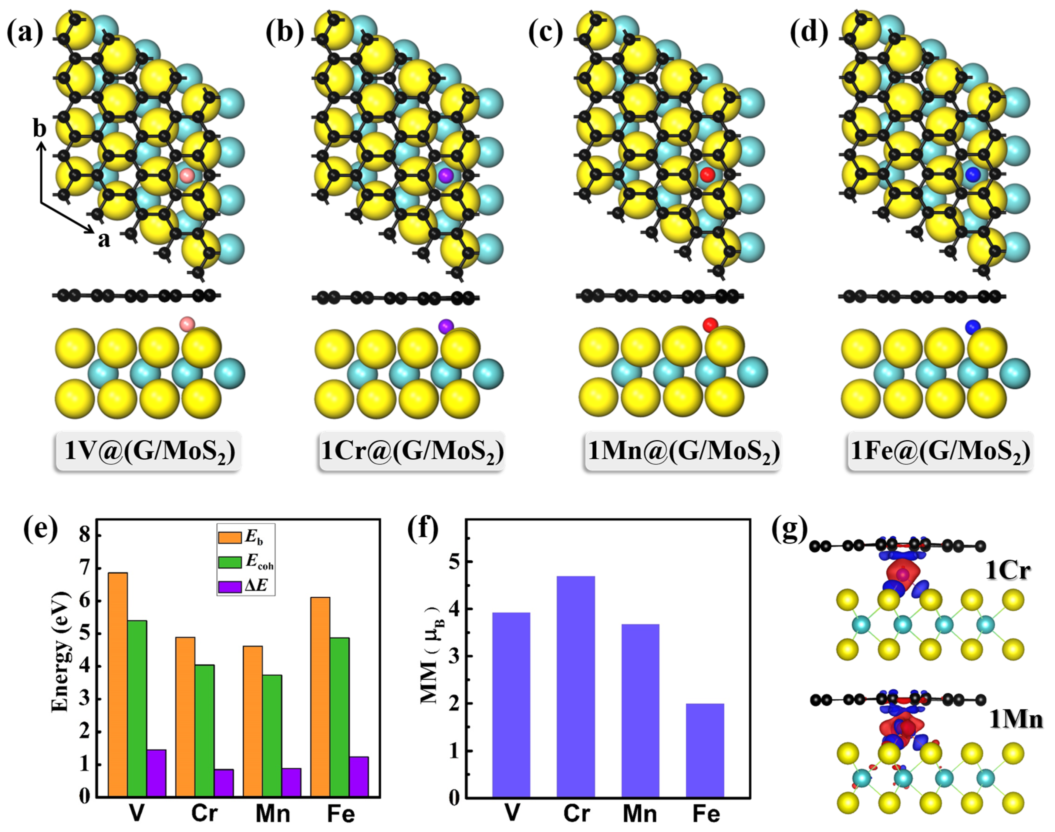
2. Results and Discussion

First, we explored the structures and electronic properties of single TM atom-intercalated G/MoS2, 1TM@(G/MoS2) (TM = V, Cr, Mn, Fe). Three types of intercalated sites for locating TM atoms were tested for all the 1TM@(G/MoS2) systems (see Figure S1 in the Supplementary Materials): (i) a H-Mo site, in which the intercalated TM atom sits on the top site of a Mo atom and under the hollow site of graphene; (ii) a H-C site, in which the intercalated TM atom sits on the hollow site of MoS2 and under the C atom; and (iii) a H-H site, in which the intercalated TM atom sits between the hollow site of MoS2 and graphene. Our results proved that the single TM atom in the interlayer favors sitting in the H-Mo site, and the optimized structures of 1TM@(G/MoS2)s (TM = Ti, V, Cr, Mn) are shown in Figure 1a–d. Clearly, no significant distortion was found for all the studied systems. The distances of TM atoms to the graphene layer and MoS2 layer were 1.80/1.40 Å, 1.83/1.44 Å, 1.78/1.41 Å, and 1.96/1.33 Å for TM = Ti, V, Cr, and Mn, respectively.
To determine the structural stabilities of these 1TM@(G/MoS2)s (nTMs), we calculate the binding energy (Eb) of the TM atom relative to the graphene layer and MoS2 layer using the following formula:
Eb = [EG + EMoS2 + nETMEnTM@(G/MoS2)]/n
where EG, EMoS2, ETM, and EnTM@(G/MoS2) are the energies of the graphene layer, MoS2 layer, TM atom, and nTM@(G/MoS2), respectively, and n is the number of TM atoms. As shown in Figure 1e, the binding energy of these 1TM@(G/MoS2)s is quite large, ~4.61 eV–~6.89 eV, which is larger than that of individual TMs adsorbed on graphene [37] or MoS2 [38] monolayers. Thus, our results suggest that all the 1TM@(G/MoS2)s are thermodynamically stable. Furthermore, we find that Ebs are sensitive to the choice of TM elements, i.e., Eb with V and Fe atoms is larger than with Cr and Mn atoms. The relatively low stabilities for 1Cr@(G/MoS2) and 1Mn@(G/MoS2) can be attributed to the half-occupied feature of their outermost electrons (Cr: 3d54s1 and Mn: 3d54s2). It is known that isolated metal atoms tend to aggregate into clusters due to high surface free energy [39]. To assess the feasibility of TM atom agglomeration, we compare the cohesive energy (Ecoh) of TM atoms in their metal crystal and Ebs. The positive energy difference (ΔE = EcohEb) (see Figure 1e) means that the single TM atom is energetically more favorable than in the bulk form and is less likely to aggregate into clusters between the graphene and MoS2 layer.
To explicitly elucidate the bonding characteristics of the nTM@(G/MoS2)s systems, we calculated the charge density difference (CDD) as defined below:
Δ ρ = ρ [ n T M @ ( G / M o S 2 ) ] ρ [ n T M ] ρ [ G ] ρ [ MoS 2 ]
where ρ[·] is the charge density of the whole system, nTM atom, graphene layer, and MoS2 layer, respectively. The CDD plots of 1Cr@(G/MoS2) and 1Mn@(G/MoS2) are plotted in Figure 1g, in which the Cr (Mn) atom loses electrons while the G and MoS2 monolayers gain electrons. Detailed charges transferred to graphene and MoS2 monolayers in all the studied 1TM@(G/MoS2) heterostructures are summarized in Table 1; from TM = V to Fe, the charge transferred to the monolayer on both sides decreases gradually.
Figure 2a–d plots the partial density of states (PDOS) and spin density of these 2D 1TM@(G/MoS2) heterostructures. Interestingly, the band gap of graphene is opened in these systems, with a significant band gap of about 0.37 eV, 0.28 eV, 0.30 eV, and 0.094 eV for TM = V, Cr, Mn, and Fe, respectively, which is much larger than those of G/MoS2 heterostructures without intercalation [40,41]. Moreover, contrary to the nonmagnetic nature of the initial host [11], the intercalation of TM atom introduces magnetic properties to 1TM@(G/MoS2)s. For example, the magnetic moments of 1TM@(G/MoS2)s are 3.93 µB, 4.70 µB, 3.69 µB, and 2.00 µB for TM = V, Cr, Mn, and Fe, respectively. In addition, the charge transfer from the TM to the two-sided monolayers causes spin polarization in the graphene (MoS2) monolayer, whose local magnetic moment is around 0.02(0.48), 0.004(0.20), 0.06(0.26), and 0.06(0.24) for TM = V, Cr, Mn, and Fe, respectively. Particularly, 1Fe@(G/MoS2) is a Dirac half-metal, having a Dirac cone in the majority-spin channel while exhibiting a 94 meV gap in the minority-spin channel (see Figure 2d and Figure S2).
Furthermore, to explore the effect of different TM ratios on the electronic and magnetic properties of these TM-intercalated G/MoS2 systems, we investigated the G/MoS2 heterostructures of two- and three-TM atomic intercalations nTM@(G/MoS2) (TM = V, Cr, Mn, Fe, n = 2, 3). For 2TM@(G/MoS2)s and 3TM@(G/MoS2)s, nine and six isomers with different TM atom arrangements were tested, respectively (see Figures S3–S10). For the former, the lowest energy structure of the system with TM = V, Cr, Mn is that of two TM atoms sitting in two adjacent hollow positions in graphene along the zigzag direction (see Figure 3a–c), whereas for 2Fe@(G/MoS2), the two Fe atoms prefer to sit a bit further away, i.e., they sit in two adjacent hollow positions in graphene along the armchair direction. For the latter, similar conformations were found for the most stable 3V@(G/MoS2) and 3Mn@(G/MoS2), where the three TM atoms are located on three adjacent hollow sites of the graphene forming a “<”-shaped pattern (see Figure 3e,g). As for 3Cr@(G/MoS2), the shape of the three Cr atoms was found to be almost linear, with two of the end Cr atoms located at the edge sites of the graphene, leaving the middle Cr atom located at the hollow site (see Figure 3f). For 3Fe@(G/MoS2), two of the three Fe atoms sit far from each other, forming an “L” shape (see Figure 3h). Similar to 1TM@(G/MoS2)s, no significant structure deformation is found for the graphene layer or MoS2 layer. Except for 2(3)Fe@(G/MoS2) and 3Cr@(G/MoS2), with TM atoms sitting at a different height along the z axis, all the TM atoms are found to stay in one plane. Moreover, the G/MoS2 interlayer distances (d) of these nTM@(G/MoS2)s are found to increase with the number of TM atoms (see Table 1), i.e., d1TM@(G/MoS2) < d2TM@(G/MoS2) < d3TM@(G/MoS2).
As shown in Table 1 and Figure 4a, the binding energies per TM atom for these 2TM@(G/MoS2)s and 3TM@(G/MoS2)s are 6.03/5.70 eV, 4.08/3.79 eV, 4.02/3.72 eV, and 5.23/5.15 eV for TM = V, Cr, Mn, and Fe, respectively, which are smaller than those of the 1TM@(G/MoS2)s. We note that the Ebs per TM atom for these nTM@(G/MoS2)s is related to the ratio of intercalated TM atoms, i.e., the higher the TM ratio, the smaller the Ebs per TM atom. Our results show that single TM atom intercalation is the most energetically favorable in all systems. This stability related to the TM ratio is consistent with the transferred charge between the TM atoms and the two face layers, i.e., ΔQ1 + ΔQ2 decreases as n increases from 1 to 3 (see Table 1 and Figure 4b,c). Furthermore, as n increases, the charge redistribution around the TM atoms is no longer equivalent to their different positional sites (see inset in Figure 4b,c).
The PDOS and spin density plots of these 2TM@(G/MoS2)s and 3TM@(G/MoS2)s are shown in Figure 5. Similar to 1TM@(G/MoS2)s, the systems intercalated with two or three TM atoms are magnetic, with their magnetic moments mainly contributed to by 3d orbitals of TM atoms. Our results show that the magnetic moments of 2TM@(G/MoS2)s and 3TM@(G/MoS2)s are nearly double or triple those of 1TM@(G/MoS2)s. For the former, they are around 5.81 µB, 10.51 µB, 6.83 µB, and 5.12 µB for TM = V, Cr, Mn, and Fe, respectively, while for the latter, they are 9.64 µB, 14.73 µB, 10.63 µB, and 8.26 µB for TM = V, Cr, Mn, and Fe, respectively. Moreover, the spin polarization of graphene and MoS2 monolayers increases as the number of TM atoms increases. On one hand, the local moments of graphene and MoS2 monolayers in 2TM@(G/MoS2)s/3TM@(G/MoS2)s are increased to 0.03(0.03)/0.02(0.33), 0.02(1.00)/0.14(0.58), 0.006(1.16)/0.10(1.29), and 0.05(0.29)/0.06(0.19) for TM = V, Cr, Mn, and Fe, respectively. On the other hand, the larger spin polarization reduces the band gap in graphene, as shown in Figure 5; the band gaps of graphene in 2TM@(G/MoS2)s/3TM@(G/MoS2)s are 0.30/0.21 eV, 0.21/0.0 eV, 0.24/0.16 eV, and 0.26/0.27 eV for TM = V, Cr, Mn, and Fe, respectively. Therefore, we can conclude that the electronic and magnetic properties can be manipulated by varying the ratio of intercalated TM atoms, which is feasible in experiments through control of electrochemical voltage [20].

3. Computational Methods

All the spin-polarized density functional theory (DFT) calculations were performed with the Vienna ab initio simulation package (VASP) [42]. The ion–electron interactions were described using the projected-augmented wave (PAW) method [43]. DFT-D2, a semi-empirical method, was used to consider the van der Waals (vdW) interactions [44]. The exchange-correlation potentials were obtained using generalized gradient approximation (GGA) as parameterized by Perdew, Burke, and Ernzerhof (PBE) [45]. The energy cut-off for the plane-wave basis set was set to 400 eV. The energy convergence threshold was 10−6 eV per unit cell, and the ionic force on all relaxed atoms was less than 0.01 eV/Å. A vacuum layer of about 15 Å was used along the z direction to avoid interactions between neighboring cells. To consider the 3d electron’s strong correlation effect, a GGA + U method [46] was adopted with U = 3 eV in accordance with previous studies [47,48]. The graphene/MoS2 heterostructure (G/MoS2) was constructed as periodic slabs with the lattice parameters a = b = 12.35 Å, in which a 5 × 5 slab of graphene and 4 × 4 slab of the MoS2 monolayer were employed. One, two, and three TM atoms were intercalated into the interlayer gap of G/MoS2 heterostructures, which is denoted as nTM@ (G/MoS2) (n = 1, 2, 3). A Monkhorst–Pack grid of 5 × 5 × 1 was used for geometrical optimization of all the systems, and much denser k-point grids of 15 × 15 × 1 were used to explore electronic properties.

4. Conclusions

In conclusion, the electronic and magnetic properties of TM-intercalated G/MoS2 heterojunctions were systematically studied. Our results revealed that all the nTM@(G/MoS2)s (TM = Ti, V, Cr, Mn, n = 1–3) are very stable and have large binding energies. On one hand, all the studied systems are ferromagnetic, and their magnetic moments increase with n. In addition, spin polarization was observed in the graphene layer and MoS2 layer, and the degree of polarization increased with TM concentration. On the other hand, a significant band gap is opened for graphene upon the introduction of TM atoms, and the band gap is found to reduce with n due to the enhanced spin polarization of graphene. These results show that intercalation at different concentrations is a powerful approach for manipulating the electronic and magnetic properties of 2D vdW heterostructures and is thus expected to be widely applicable to other 2D layer materials and beyond.

Supplementary Materials

The following supporting information can be downloaded at: https://www.mdpi.com/article/10.3390/molecules28020509/s1, Figure S1: Optimized structures of V (a, b, c), Cr (d, e, f), Mn (g, h, i), and Fe (j, k, l) at different adsorption sites in the G/MoS2 gap, Figure S2: The spin-resolved band structure of 1Fe@(G/MoS2), Figure S3: Optimized structures of two V atoms at different adsorption sites in the G/MoS2 gap, Figure S4: Optimized structures of two Cr atoms at different adsorption sites in the G/MoS2 gap, Figure S5: Optimized structures of two Mn atoms at different adsorption sites in the G/MoS2 gap, Figure S6: Optimized structures of two Fe atoms at different adsorption sites in the G/MoS2 gap, Figure S7: Optimized structures of three V atoms at different adsorption sites in the G/MoS2 gap, Figure S8: Optimized structures of three Cr atoms at different adsorption sites in the G/MoS2 gap, Figure S9: Optimized structures of three Mn atoms at different adsorption sites in the G/MoS2 gap, Figure S10: Optimized structures of three Fe atoms at different adsorption sites in the G/MoS2 gap.

Author Contributions

Conceptualization, F.W.; methodology, Z.W. and J.H.; Software, Z.L. and L.M.; investigation, F.W.; writing—original draft preparation, F.W.; writing—review and editing, X.Z. All authors have read and agreed to the published version of the manuscript.

Funding

This work is supported by open funds from the State Key Laboratory of Rare Earth Resource Utilization (RERU2021011) and the Six Talent Peaks Project in Jiangsu Province (XCL−104).

Institutional Review Board Statement

Not applicable.

Informed Consent Statement

Not applicable.

Data Availability Statement

All relevant data are contained in the present manuscript.

Conflicts of Interest

The authors declare no conflict of interest.

Sample Availability

Not applicable.

References

  1. Habib, M.R.; Liang, T.; Yu, X.; Pi, X.; Liu, Y.; Xu, M. A review of theoretical study of graphene chemical vapor deposition synthesis on metals: Nucleation, growth, and the role of hydrogen and oxygen. Rep. Prog. Phys. 2018, 81, 036501. [Google Scholar] [CrossRef] [PubMed]
  2. Han, G.H.; Duong, D.L.; Keum, D.H.; Yun, S.J.; Lee, Y.H. van der Waals metallic transition metal dichalcogenides. Chem. Rev. 2018, 118, 6297–6336. [Google Scholar] [CrossRef]
  3. Radisavljevic, B.; Radenovic, A.; Brivio, J.; Giacometti, V.; Kis, A. Single-layer MoS2 transistors. Nat. Nanotechnol. 2011, 6, 147–150. [Google Scholar] [CrossRef] [PubMed]
  4. Li, L.; Yu, Y.; Ye, G.J.; Ge, Q.; Ou, X.; Wu, H.; Feng, D.; Chen, X.H.; Zhang, Y. Black phosphorus field-effect transistors. Nat. Nanotechnol. 2014, 9, 372–377. [Google Scholar] [CrossRef] [Green Version]
  5. Abellán, G.; Wild, S.; Lloret, V.; Scheuschner, N.; Gillen, R.; Mundloch, U.; Maultzsch, J.; Varela, M.; Hauke, F.; Hirsch, A. Fundamental Insights into the Degradation and Stabilization of Thin Layer Black Phosphorus. J. Am. Chem. Soc. 2017, 139, 10432–10440. [Google Scholar] [CrossRef] [Green Version]
  6. Ma, Y.; Dai, Y.; Wei, W.; Niu, C.; Yu, L.; Huang, B. First-Principles Study of the Graphene@MoSe2 Heterobilayers. J. Phys. Chem. C 2011, 115, 20237–20241. [Google Scholar] [CrossRef]
  7. Hwang, B.; Hwang, J.; Yoon, J.K.; Lim, S.; Kim, S.; Lee, M.; Kwon, J.H.; Baek, H.; Sung, D.; Kim, G.; et al. Energy Bandgap and Edge States in an Epitaxially Grown Graphene/h-BN Heterostructure. Sci. Rep. 2016, 6, 31160. [Google Scholar] [CrossRef] [Green Version]
  8. Kochaev, A.; Katin, K.; Maslov, M.; Meftakhutdinov, R. AA-Stacked Borophene-Graphene Bilayer with Covalent Bonding: Ab Initio Investigation of Structural, Electronic and Elastic properties. J. Phys. Chem. Lett. 2020, 11, 5668–5673. [Google Scholar] [CrossRef]
  9. Geim, A.K.; Grigorieva, I.V. Van der Waals heterostructures. Nature 2013, 499, 419–425. [Google Scholar] [CrossRef] [Green Version]
  10. Dean, C.R.; Young, A.F.; Cadden-Zimansky, P.; Wang, L.; Ren, H.; Watanabe, K.; Taniguchi, T.; Kim, P.; Hone, J.; Shepard, K.L. Multicomponent fractional quantum Hall effect in graphene. Nat. Phys. 2011, 7, 693–696. [Google Scholar] [CrossRef]
  11. Neupane, H.K.; Adhikari, N.P.; Hang, D.-R. Tuning Structural, Electronic, and Magnetic Properties of C Sites Vacancy Defects in Graphene/MoS2 van der Waals Heterostructure Materials: A First-Principles Study. Adv. Condens. Matter. Phys. 2020, 2020, 8850701. [Google Scholar] [CrossRef]
  12. Zhou, Y.; Yang, P.; Zu, H.; Gao, F.; Zu, X. Electronic Structures and Magnetic Properties of MoS2 Nanostructures: Atomic Defects, Nanoholes, Nanodots and Antidots. Phys. Chem. Chem. Phys. 2013, 15, 10385–10394. [Google Scholar] [CrossRef] [PubMed]
  13. Fu, S.; Wang, D.; Ma, Z.; Liu, G.; Zhu, X.; Yan, M.; Fu, Y. The first-principles study on the halogen-doped graphene/MoS2 heterojunction. Solid State Commun. 2021, 334–335, 114366. [Google Scholar] [CrossRef]
  14. Shu, H.; Luo, P.F.; Liang, P.; Cao, D.; Chen, X.S. Layer-Dependent Dopant Stability and Magnetic Exchange Coupling of Iron-Doped MoS2 Nanosheets. ACS Appl. Mater. Interfaces 2015, 7, 7534–7541. [Google Scholar] [CrossRef] [PubMed]
  15. Shi, J.; Chen, L.; Yang, M.; Mi, Z.; Zhang, M.; Gao, K.; Zhang, D.; Su, S.; Hou, W. Interface contact and modulated electronic properties by external vertical strains and electric fields in graphene/MoS2 heterostructure. Curr. Appl. Phys. 2022, 39, 331–338. [Google Scholar] [CrossRef]
  16. Ghorbani-Asl, M.; Bristowe, P.D.; Koziol, K.; Heine, T.; Kuc, A. Effect of compression on the electronic, optical and transport properties of MoS2/graphene-based junctions. 2D Mater. 2016, 3, 025018. [Google Scholar] [CrossRef]
  17. Manchanda, P.; Sharma, V.; Yu, H.; Sellmyer, D.J.; Skomski, R. Magnetism of Ta Dichalcogenide Monolayers Tuned by Strain and Hydrogenation. Appl. Phys. Lett. 2015, 107, 032402. [Google Scholar] [CrossRef] [Green Version]
  18. Larson, D.T.; Fampiou, I.; Kim, G.; Kaxiras, E. Lithium intercalation in graphene–MoS2 heterostructures. J. Phys. Chem. C 2018, 122, 24535–24541. [Google Scholar] [CrossRef]
  19. Jung, Y.; Zhou, Y.; Cha, J.J. Intercalation in Two-Dimensional Transition Metal Chalcogenides. Inorg. Chem. Front. 2016, 3, 452–463. [Google Scholar] [CrossRef]
  20. Wan, J.; Lacey, S.D.; Dai, J.; Bao, W.; Fuhrer, M.S.; Hu, L. Tuning two-dimensional nanomaterials by intercalation: Materials, properties and applications. Chem. Soc. Rev. 2016, 45, 6742–6765. [Google Scholar] [CrossRef]
  21. Stark, M.S.; Kuntz, K.L.; Martens, S.J.; Warren, S.C. Intercalation of Layered Materials from Bulk to 2D. Adv. Mater. 2019, 31, e1808213. [Google Scholar] [CrossRef]
  22. Ghosh, D.; Devi, P.; Kumar, P. Intercalation in two-dimensional transition metal chalcogenides: Interlayer engineering and applications. Prog. Energy 2022, 4, 022001. [Google Scholar] [CrossRef]
  23. Zhou, J.; Lin, Z.; Ren, H.; Duan, X.; Shakir, I.; Huang, Y.; Duan, X. Layered Intercalation Materials. Adv. Mater. 2021, 33, e2004557. [Google Scholar] [CrossRef] [PubMed]
  24. Kühne, M.; Börrnert, F.; Fecher, S.; Ghorbani-Asl, M.; Biskupek, J.; Samuelis, D.; Krasheninnikov, A.V.; Kaiser, U.; Smet, J.H. Reversible superdense ordering of lithium between two graphene sheets. Nature 2018, 564, 234–239. [Google Scholar] [CrossRef]
  25. Zhu, G.; Liu, J.; Zheng, Q.; Zhang, R.; Li, D.; Banerjee, D.; Cahill, D.G. Tuning thermal conductivity in molybdenum disulfide by electrochemical intercalation. Nat. Commun. 2016, 7, 13211. [Google Scholar] [CrossRef] [PubMed] [Green Version]
  26. Kang, J.S.; Ke, M.; Hu, Y. Ionic Intercalation in Two-Dimensional van der Waals Materials: In Situ Characterization and Electrochemical Control of the Anisotropic Thermal Conductivity of Black Phosphorus. Nano Lett. 2017, 17, 1431–1438. [Google Scholar] [CrossRef]
  27. Zhang, J.; Yang, A.; Wu, X.; van de Groep, J.; Tang, P.; Li, S.; Liu, B.; Shi, F.; Wan, J.; Li, Q.; et al. Reversible and selective ion intercalation through the top surface of few-layer MoS2. Nat. Commun. 2018, 9, 5289. [Google Scholar] [CrossRef] [PubMed] [Green Version]
  28. Ng, H.K.; Abutaha, A.; Voiry, D.; Verzhbitskiy, I.; Cai, Y.; Zhang, G.; Liu, Y.; Wu, J.; Chhowalla, M.; Eda, G.; et al. Effects of Structural Phase Transition on Thermoelectric Performance in Lithium-Intercalated Molybdenum Disulfide (LixMoS2). ACS Appl. Mater. Interfaces 2019, 11, 12184–12189. [Google Scholar] [CrossRef] [PubMed]
  29. Profeta, G.; Calandra, M.; Mauri, F. Phonon-mediated superconductivity in graphene by lithium deposition. Nat. Phys. 2012, 8, 131–134. [Google Scholar] [CrossRef] [Green Version]
  30. Xiong, F.; Wang, H.; Liu, X.; Sun, J.; Brongersma, M.; Pop, E.; Cui, Y. Li Intercalation in MoS2: In Situ Observation of Its Dynamics and Tuning Optical and Electrical Properties. Nano Lett. 2015, 15, 6777–6784. [Google Scholar] [CrossRef]
  31. Bediako, D.K.; Rezaee, M.; Yoo, H.; Larson, D.T.; Zhao, S.Y.F.; Taniguchi, T.; Watanabe, K.; Brower-Thomas, T.L.; Kaxiras, E.; Kim, P. Heterointerface effects in the electrointercalation of van der Waals heterostructures. Nature 2018, 558, 425–429. [Google Scholar] [CrossRef] [PubMed] [Green Version]
  32. Zhang, X.; Zhao, X.; Liu, Y. Ab Initio Study of Structural, Electronic, and Magnetic Properties of Transition Metal Atoms Intercalated AA-Stacked Bilayer Graphene. J. Phys. Chem. C 2016, 120, 22710–22717. [Google Scholar] [CrossRef]
  33. Zhang, X.; Xu, W.; Dai, J.; Liu, Y. Role of embedded 3d transition metal atoms on the electronic and magnetic properties of defective bilayer graphene. Carbon 2017, 118, 376–383. [Google Scholar] [CrossRef]
  34. Zhang, X.; Sun, Y.; Ma, L.; Zhao, X.; Yao, X. Modulating the electronic and magnetic properties of bilayer borophene via transition metal atoms intercalation: From metal to half metal and semiconductor. Nanotechnology 2018, 29, 305706. [Google Scholar] [CrossRef]
  35. Zhang, X.; Bao, Z.; Ye, X.; Xu, W.; Wang, Q.; Liu, Y. Half-metallic properties of 3d transition metal atom-intercalated graphene@MS2 (M = W, Mo) hybrid structures. Nanoscale 2017, 9, 11231–11238. [Google Scholar] [CrossRef] [PubMed]
  36. Zhang, X.; Sun, Y.; Gao, W.; Lin, Y.; Zhao, X.; Wang, Q.; Yao, X.; He, M.; Ye, X.; Liu, Y. Sizable bandgaps of graphene in 3d transition metal intercalated defective graphene/WSe2 heterostructures. RSC Adv. 2019, 9, 18157–18164. [Google Scholar] [CrossRef] [Green Version]
  37. Krasheninnikov, A.V.; Lehtinen, P.O.; Foster, A.S.; Pyykko, P.; Nieminen, R.M. Embedding transition-metal atoms in graphene: Structure, bonding, and magnetism. Phys. Rev. Lett. 2009, 102, 126807. [Google Scholar] [CrossRef] [Green Version]
  38. Wang, X.-Q.; Chen, W.-G.; Zhu, Z.-L.; Jia, Y. Electronic and Magnetic Properties Modulated by Adsorption of 3d Transition Metal Atoms in Monolayer and Bilayer MoS2 Sheets. Acta Metall. Sin. 2015, 28, 793. [Google Scholar] [CrossRef] [Green Version]
  39. Yang, X.-F.; Wang, A.; Qiao, B.; Li, J.; Liu, J.; Zhang, T. Single-Atom Catalysts: A New Frontier in Heterogeneous Catalysis. Acc. Chem. Res. 2013, 46, 1740. [Google Scholar] [CrossRef]
  40. Wang, Z.; Chen, Q.; Wang, J. Electronic Structure of Twisted Bilayers of Graphene/MoS2 and MoS2/MoS2. J. Phys. Chem. C 2015, 119, 4752. [Google Scholar] [CrossRef]
  41. Jin, C.; Rasmussen, F.A.; Thygesen, K.S. Tuning the Schottky Barrier at the Graphene/MoS2 Interface by Electron Doping: Density Functional Theory and Many-Body Calculations. J. Phys. Chem. C 2015, 119, 19928. [Google Scholar] [CrossRef]
  42. Kresse, G.; Furthmüller, J. Efficiency of ab-initio total energy calculations for metals and semiconductors using a plane-wave basis set. Comp. Mater. Sci. 1996, 6, 15–50. [Google Scholar] [CrossRef]
  43. Blöchl, P.E. Projector augmented-wave method. Phys. Rev. B 1994, 50, 17953–17979. [Google Scholar] [CrossRef] [PubMed] [Green Version]
  44. Bučko, T.; Hafner, J.; Lebègue, S.; Ángyán, J.G. Improved Description of the Structure of Molecular and Layered Crystals: Ab Initio DFT Calculations with van der Waals Corrections. J. Phys. Chem. A 2010, 114, 11814–11824. [Google Scholar] [CrossRef]
  45. Perdew, J.P.; Burke, K.; Ernzerhof, M. Generalized Gradient Approximation Made Simple. Phys. Rev. Lett. 1996, 77, 3865–3868. [Google Scholar] [CrossRef] [PubMed] [Green Version]
  46. Liechtenstein, A.; Anisimov, V.I.; Zaanen, J. Density-functional theory and strong interactions: Orbital ordering in Mott-Hubbard insulators. Phys. Rev. B 1995, 52, R5467. [Google Scholar] [CrossRef] [Green Version]
  47. Yao, X.; Wang, L.; Sun, Y.; Li, X.; Sun, J.; Wang, B.; He, M.; Zhang, X. Two-dimensional transition metal triborides: Monolayers with robust intrinsic magnetism and high spin stability. Phys. Rev. B 2022, 105, 214421. [Google Scholar] [CrossRef]
  48. Dou, M.; Li, H.; Yao, Q.; Wang, J.; Liu, Y.; Wu, F. Room-temperature ferromagnetism in two-dimensional transition metal borides: A first-principles investigation. Phys. Chem. Chem. Phys. 2021, 23, 10615. [Google Scholar] [CrossRef]
Figure 1. (ad) The lowest energy structures of 1TM@(G/MoS2) (TM = Ti, V, Cr, Mn). Green, yellow, black, pink, purple, red, and blue balls represent Mo, S, C, V, Cr, Mn, and Fe atoms, respectively. (e) The binding energy (Eb) of one TM atom between G and MoS2, the cohesive energy of TM atoms in their metal crystals (Ecoh), and the energy difference between them (ΔE = EcohEb). (f) Magnetic moments (MM) of 1TM@(G/MoS2). (g) The charge density difference (CDD) plots of 1Cr@(G/MoS2) and 1Mn@(G/MoS2).
Molecules 28 00509 g001
Figure 2. (ad) Partial density of states (PDOS) and spin density plots for 1TM@(G/MoS2) (TM = Ti, V, Cr, Mn). The left and right panels of every PDOS plot are the minority- and majority-spin channels, respectively.
Molecules 28 00509 g002
Figure 3. The lowest energy structures of (ad) 2TM@(G/MoS2) and (eh) 3TM@(G/MoS2) (TM = Ti, V, Cr, Mn).
Molecules 28 00509 g003
Figure 4. (a) The binding energy (Eb) of two TM atoms and three TM atoms in-between G and MoS2. (b,c) The charges transferred from TM atoms to G and MoS2 for 2TM@(G/MoS2) and 3TM@(G/MoS2). (d) Magnetic moments (MM) of 2TM@(G/MoS2) and 3TM@(G/MoS2).
Molecules 28 00509 g004
Figure 5. Partial density of states (PDOS) and spin density plots for (ad) 2TM@(G/MoS2) and (eh) 3TM@(G/MoS2) (TM = Ti, V, Cr, Mn).
Molecules 28 00509 g005
Table 1. Distances between the graphene layer and MoS2 layer (d, Å), the binding energies (Eb, eV), charges transferred from TM atoms to graphene (ΔQ1, e) and MoS2 (ΔQ2, e), and magnetic moments (MM, µB).
1TM@(G/MoS2)2TM@(G/MoS2)3TM@(G/MoS2)
dEbΔQ1/ΔQ2MMdEbΔQ1/ΔQ2MMdEbΔQ1/ΔQ2MM
V3.206.860.46/0.663.933.536.030.43/0.645.813.595.700.42/0.649.64
Cr3.274.890.41/0.654.703.744.080.36/0.5510.513.803.790.33/0.5814.73
Mn3.194.620.38/0.573.693.524.020.30/0.496.833.643.720.24/0.5010.63
Fe3.296.110.12/0.562.003.525.230.26/0.415.123.575.150.21/0.428.26
Disclaimer/Publisher’s Note: The statements, opinions and data contained in all publications are solely those of the individual author(s) and contributor(s) and not of MDPI and/or the editor(s). MDPI and/or the editor(s) disclaim responsibility for any injury to people or property resulting from any ideas, methods, instructions or products referred to in the content.

