Abstract
This paper shows the fabrication of a new environmentally friendly sensor, an activated glassy carbon electrode with an in situ deposited bismuth film (aGCE/BiF), to determine Cd(II) and Pb(II) at the nanotrace level. The electrochemical activation of the GCE surface was achieved in a solution of 0.1 M phosphate-buffered saline (PBS) of pH = 7 by performing five cyclic voltammetric scans in the range of −1.5–2.5 V at ν of 100 mV/s. The newly developed electrode provides several advantages, such as an increased electron active surface (compared to the glassy carbon electrode) and improved electron transfer kinetics. As a result, the new voltammetric procedure (square-wave anodic stripping voltammetry, SWASV) was established and optimized. With the SWASV method, the following calibration curves and low detection limits (LODs) were obtained for Cd(II) and Pb(II), respectively: 5–100 nM, 0.62 nM, 2–200 nM, and 0.18 nM. The newly prepared method was used to determine the amounts of Pb(II) and Cd(II) in the certified reference material, and the results agreed with the certified values. Moreover, the procedure was successfully applied to determine the Cd(II) and Pb(II) in river samples. The official and standard addition methods validated the measurement results.
1. Introduction
Heavy metals are a group of substances that pollute the environment. They are characterized by a high molar mass, high density, and toxicity to living organisms. Typical examples are copper, lead, nickel, iron, and cadmium. They are highly toxic and remain in the atmosphere for a long time, so they can accumulate in the human body through so-called bioaccumulation. These compounds may enter terrestrial and aquatic environments, causing pollution, and once they enter some environments, they are very difficult to completely remove. The aquatic environment can be polluted with heavy metals in many ways, including the burning of fossil fuels, vehicle exhaust gases, mining, agriculture, and the burning of solid and liquid waste. In the air, heavy metals can occur naturally due to the activities of volcanoes, thermal springs, erosion, infiltration, etc. Over the last few years, there has been a lot of interest in studying the impacts of these toxic agents because human health is ubiquitously exposed to the effects of these compounds. Unfortunately, heavy metals are commonly used in everyday life, for example, in electrical devices and industry, and environmental pollution with these metals has become a serious problem. In general, the toxicity of metal ions is due to their chemical nature. They can react with cellular structural proteins, enzymes, and membrane systems and can block their biological activity. They can enter the organs of a living organism and accumulate, and the amount of metal that can be deposited depends on the route of exposure and the chemical properties of the metal such as its valency state, volatility, lipid solubility, etc. Recently, it has been shown that some heavy metals such as chromium, nickel, or lead may contribute to the development of cancer. In this paper, we would like to focus primarily on the negative impact of cadmium and lead [1,2,3].
People are exposed to cadmium through inhalation of polluted air and ingestion. The kidneys and bones are mainly at risk, where cadmium can accumulate. This metal can also cause lung damage, mainly in tobacco smokers. For non-smokers, cadmium poisoning may occur due to an improper diet (90% of cases for non-smokers). However, in the aquatic environment, cadmium is not degraded to less toxic products, which contributes to its bioaccumulation in the kidneys and livers of aquatic organisms and microflora. Interestingly, it is believed that cadmium is not necessary for the proper functioning of the human organism [2]. It is worth mentioning that cadmium can lead to an imbalance of some minerals in the human body, such as zinc, magnesium, or copper [4]. Lead, however, can cause lung cancer or stomach cancer through repeated exposure, which causes the concentration of lead in the blood to increase rapidly. Studies have also examined possible links between workplace exposure to lead and other cancers such as brain, kidney, bladder cancer, etc., but the results were mixed. Additionally, lead can cause anemia and problems with the nervous system [2]. Moreover, the FAO/WHO talks about the PTWI index, which stands for Provisional Tolerable Weekly Intake. This is the amount of a substance that does not have harmful effects on the human body. For cadmium and lead, the PTWI values are, respectively, 7 μg/kg and 25 μg/kg per kilogram bodyweight [5]. Pollution with heavy metal ions and their negative impact on living organisms are a serious environmental problem, which is why it is so important to control the concentration of these ions, in particular cadmium and lead, at the trace level.
Several analytical methods for simultaneously determining cadmium and lead are described in the literature, mainly spectroscopic ones, for example, graphite furnace atomic absorption spectrometry [6], inductively coupled plasma mass spectrometry [7], or flame atomic absorption spectrophotometry [8], in different matrices. However, voltammetric methods predominate in the vast majority of cases. Compared to spectroscopic methods, voltammetric measurements do not use expensive and complicated equipment [9]. Moreover, voltammetric methods are characterized by much higher sensitivity, faster measurements, and lower limits of detection (LODs) and quantification (LOQs). It is also worth mentioning that by using special chemical sensors, e.g., screen-printed electrodes (SPEs), you can further miniaturize the equipment and perform field analyses. Recently, there has been a tendency to use sensors whose surface has previously been modified [10,11,12,13,14,15]. This can be achieved by electrochemical deposition of a metal film, e.g., bismuth film (BiF) [11], or surfactant film such as sodium dodecylsulphate (SDS) [16], deposition of nanoparticles such as silver nanoparticles (AgNPs) [15], or polymerization of a given chemical compound [11]. Furthermore, an equally common step during sensor pre-preparation is electrochemical activation. There are many types of activation, such as treatment with a laser, vacuum heating, mechanical polishing, ultrasonication, or the carbon arc, and most of them are very-well known. Recent studies have shown that sensors such as glassy carbon electrodes (GCEs) can easily be activated by pre-anodization, which is followed by short cathodization, cathodization, or anodization at high potential. Such preparation can create surface functional groups (SFGs) [17,18]. All these steps are intended to improve the parameters that describe the electrode, such as the electron active surface, kinetics of electron transfer, or charge transfer resistance (Rct). Moreover, activation can increase the polarity of the electrode surface.
There has been great interest in bismuth-based sensors [12,19,20,21,22,23]. These electrodes have partially replaced mercury electrodes such as hanging mercury drop electrode (HMDE) or mercury film electrodes (MFEs) due to their toxicity and volatility. Sensors modified with bismuth-based materials feature properties such as a low background current, large active surface, and low charge transfer resistance. Most importantly, these electrodes are non-toxic for humans and do not cause lasting effects. In addition, bismuth-based modifiers can increase the selectivity of a voltammetric method for simultaneous determination of cadmium and lead ions due to better peak separation, e.g., reducing thallium interference [23]. Data found in the literature indicate that bismuth modifiers significantly improve the sensitivity of cadmium ion determination, and increasing the polarity of the carbon surface improves the sensitivity of lead ion determination. This is because the more favored interactions are Cd-bismuth and Pb-polar electrode surface, which can be seen in the case of determining the traces of these ions without the use of modifiers (no signal from Cd(II) and a small signal from Pb(II) on unmodified carbon electrodes) [19].
Previous methods described in the literature give results comparable to those obtained in this work (Table 1) [9,10,11,12,13,14,15,19,20,21,22,23,24,25,26,27,28]. This raises the question of where the novelty of this paper lies. All previous methods described in the literature are characterized by complicated steps in preparing the chemical sensor, long times of accumulation of the analyte on the electrode surface, or the usage of chemical reagents that are dangerous/toxic to humans or pollute the environment and cause lasting effects. To overcome those issues, we propose a method in which sensor activation is quick and simple and the measurements are characterized by simplicity, speed, and the use of non-toxic reagents such as bismuth nitrate or phosphate-buffered saline. To study the electrochemical properties of the aGCE/BiF, CV scans using the Fe(III)/Fe(II) redox system were performed. In addition, scanning electron microscopic (SEM) measurements were taken to identify differences in changes on the electrode surface before and after activation.
2. Results and Discussion
2.1. Activation of the Electrode Surface
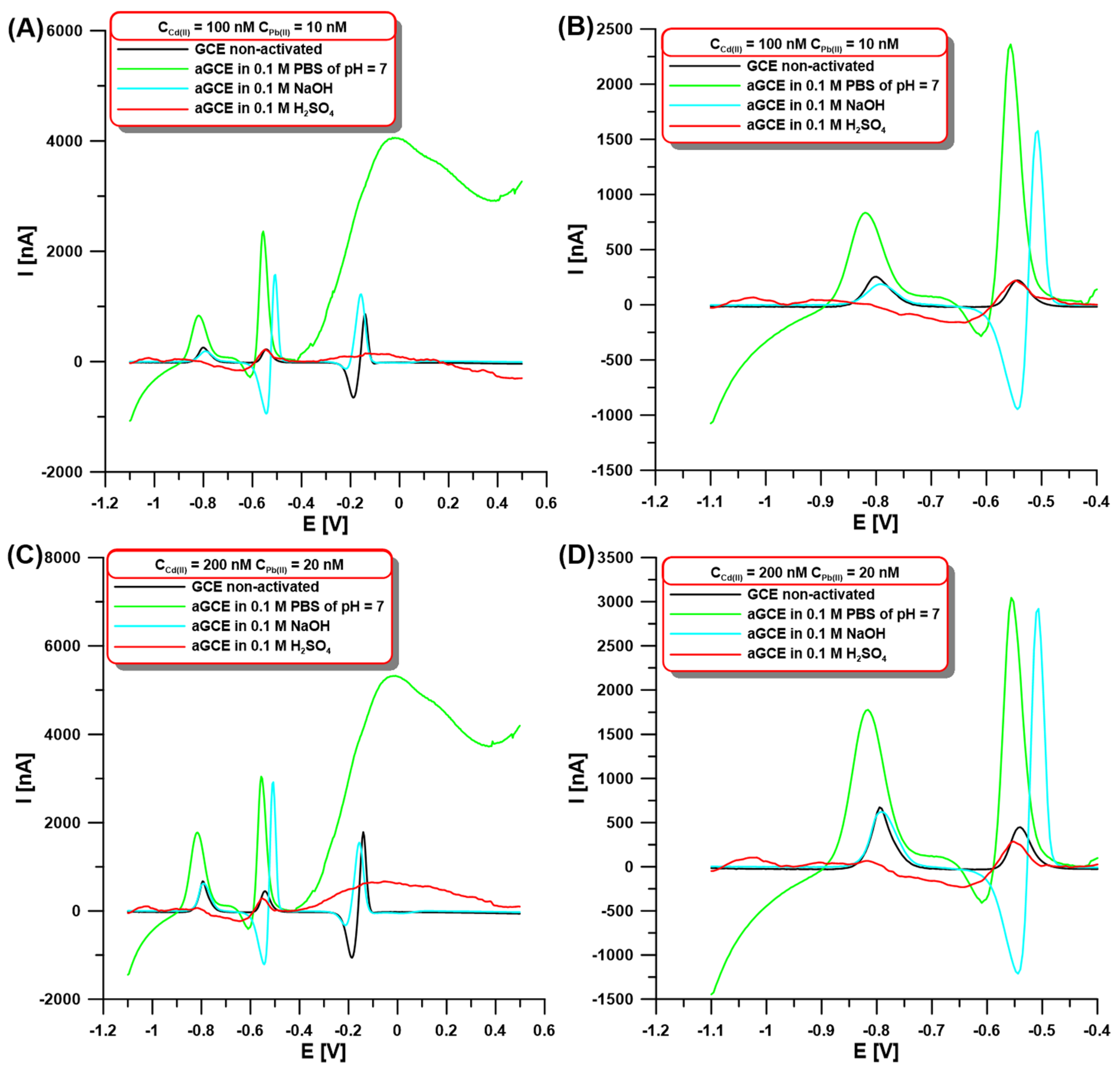
In the initial stage of the experiments, the SWASV signals of Cd(II) and Pb(II) were compared using the GCE modified with a bismuth film at non-activated (GCE/BiF) and activated electrodes on different solution surfaces (aGCE/BiF). Our goal was to check whether electrochemical activation in other solutions (0.1 M PBS of pH = 7, 0.1 M NaOH, and 0.1 M H2SO4) contributes to changes in the peak current intensity of the determined ions. The activation was performed using five cyclic voltammetric (CV) scans in the potential range of −1.5–2.5 V at a scan rate (ν) of 100 mV/s. The choice of solutions and the activation procedure were not accidental since they were based on literature data [18,29]. SWASV voltammograms were registered on both the GCE/BiF and aGCE/BiF electrodes in 0.1 M acetate buffer of pH = 4.5 containing 3.0 µM Bi(III) and 100 or 200 nM Cd(II), and 10 or 20 nM Pb(II) after 60 s accumulation at the potential of −1.1 V (Figure 1). The obtained results for both the lower and higher concentrations of Cd(II) and Pb(II) clearly show that the highest analyte signal can be obtained on the sensor activated in 0.1 M PBS of pH = 7 (Figure 1A–D, green vs. black curve). The SWASV curves (Figure 1) show peaks of Cd (around −0.8 V), Pb (around −0.55 V), and Bi (around 0 V). Small changes in the peak potentials depending on the composition of the solution used for the activation electrode were observed. Additionally, in the case of sulfuric acid, an additional peak at around −1.05 V is visible, which is related to the contamination of the electrode surface during the activation stage. The activation causes an increase in the peak current intensity of cadmium up to 283.6% for 100 nM Cd(II) and 255.6% for 200 nM Cd(II) compared to the signals obtained on the non-activated GCE/BiF. On the other hand, in the case of the lead signal, increases of up to 1233.2% (for 10 nM Pb(II)) and 856.1% (for 20 nM Pb(II)) were observed after electrochemical activation. The increase in the signals can be explained by the improvement of the electron transfer ability and enhancement of the electrochemical activity of the sensor, which is connected with the formation of oxygen-containing surface functional groups. The formation of these groups after electrochemical activation in 0.1 M PBS of pH = 7 on the GCE surface has been well-described in the literature [17,18].
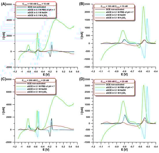
Figure 1.
The SWASV at the GCE/BiF and aGCE/BiF activated in 0.1 M PBS of pH = 7 (green curves), 0.1 M NaOH (blue curves), and 0.1 M H2SO4 (red curves) in the presence of 100 nM Cd(II) and 10 Pb(II) (A,B) or 200 nM Cd(II) and 20 nM Pb(II) (C,D). The activation was performed using 5 CVs in the potential range of −1.5–2.5 V at ν of 100 mV/s The SWASV conditions: 0.1 M acetate buffer of pH = 4.5, 3.0 µM Bi(III), electrochemical cleaning of the electrode surface at 0.5 V for 60 s, Edep.Bi+acc. of −1.1 V, tdep.Bi+acc. of 60 s, f of 25 Hz, ESW of 25 mV, and ΔE of 4 mV. The SWASV curves were registered in the potential range of −1.1–0.5 V (from (A) to (D)). (B,D) are cutouts (−1.1–(−0.4 V)) of (A) and (C), respectively.
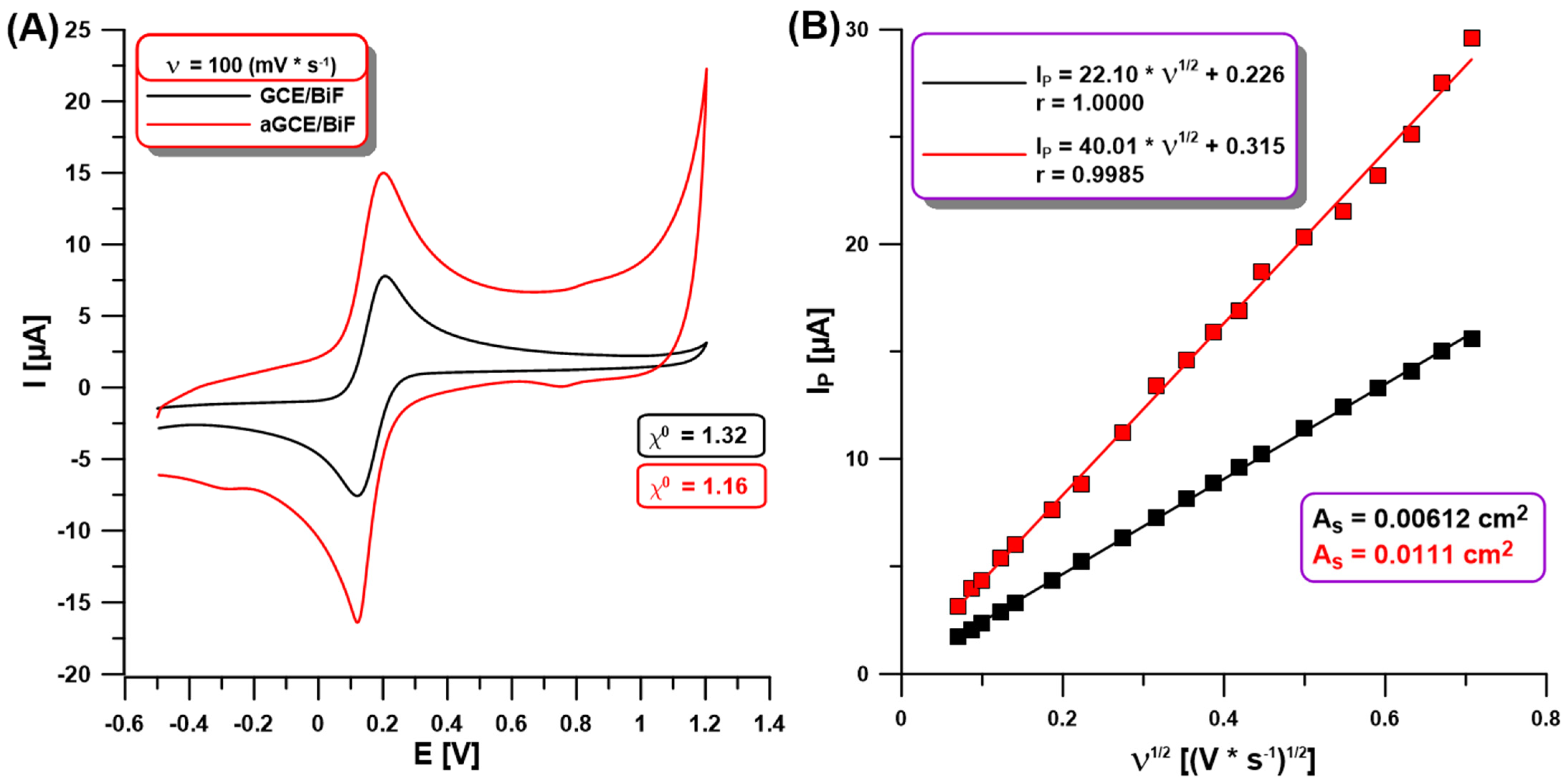
In our studies using CV in a solution of 0.1 M KCl containing 0.5 mM [Fe(CN)6]3−/4− at the GCE/BiF and aGCE/BiF activated in 0.1 M PBS of pH = 7, we showed changes between the electrochemical properties of both sensors. Figure 2A demonstrates the CVs on the non-activated GCE/BiF and activated aGCE/BiF at ν of 100 mV/s. The enhancement of the analytical signal of Fe(II) and Fe(III) at the activated electrode is visible in comparison to the non-activated one (Figure 2A,B). The calculated relative peak separation (χ0) values (1.32 for GCE/BiF vs. 1.16 for aGCE/BiF) and the electrochemically active areas (As) of the electrodes (0.00612 cm2 for the GCE/BiF vs. 0.0111 cm2 for the aGCE/BiF) clearly show an improvement in the electrochemical properties (improvement in the electron transfer between the electrode surface and the solution, and increasing the number of active sites where electrode reactions can occur) after electrochemical activation in 0.1 M PBS of pH = 7.
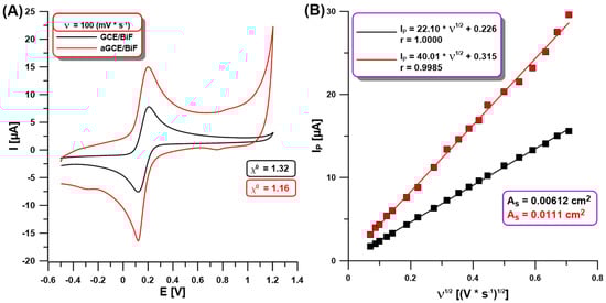
Figure 2.
(A) CVs at the GCE/BiF (black curve) and aGCE/BiF (red curve) using ν of 100 mV/s in 0.1 M KCl containing 0.5 mM [Fe(CN)6]3−/4−; (B) dependence between the anodic Ip and the square root of ν (ν1/2, ν of 5–500 mV/s) at the GCE/BiF and aGCE/BiF activated in 0.1 M PBS solution of pH = 7.0 ± 0.1 by 5 CVs in the potential range of −1.5–2.5 V (ν of 100 mV/s).
In our studies, we confirmed that the activation of the electrode in 0.1 M PBS of pH = 7 contributes to a change in the morphology of the deposited bismuth film. In the SEM images (Figure 3), significant differences can be seen in the structure of the BiF deposited onto the non-activated and activated electrode surfaces as well as in the number of particles on the surfaces (Figure 3A vs. Figure 3B). On the aGCE/BiF, bismuth particles take on various shapes, from mushroom-like formations to overlapping plates (Figure 3C,D), and the film structure is more developed since we observe a much greater number of these particles on the surface.
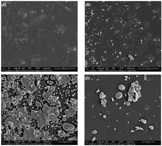
Figure 3.
SEM images of the GCE/BiF (A) and aGCE/BiF (B–D).
Figure 3.
SEM images of the GCE/BiF (A) and aGCE/BiF (B–D).

Table 1.
Comparison voltammetric procedures for the Cd(II) and Pb(II) quantification.
Table 1.
Comparison voltammetric procedures for the Cd(II) and Pb(II) quantification.
| Electrode | Technique | Linear Range [nM] | LOD [nM] | Analyzed Sample | Ref. | ||
|---|---|---|---|---|---|---|---|
| Cd(II) | Pb(II) | Cd(II) | Pb(II) | ||||
| HMDE | DPAdCSV | 1.8–266.9 | 2.4–337.8 | 0.089 | 0.082 | Food | [9] |
| CMCPE | DPASV | 250.0–25,000.0 | 100.0–15,000.0 | 40.0 | 10.0 | Water | [10] |
| SPCE/poly(BCP)/Bi | DPASV | 0–2224.0 | 0–1207.0 | 0.32 | 0.13 | Wastewater | [11] |
| GCE/BiF/NanoSiO2 | SWASV | 17.8–1334.0 | 9.7–724.0 | 5.34 | 0.96 | Water | [12] |
| BDDE | SWASV | 50.0–3985.0 | 48.0–7954.0 | 30.0 | 17.50 | - | [13] |
| GCE/MoSI | DPASV | 4.5–1334.0 | 7.2–724.0 | 0.89 | 2.17 | Tap water | [14] |
| GNs@AgNP | SWASV | 21.3–192.0 | 198.0–989.0 | 0.21 | 0.21 | Water | [15] |
| GCE/NHgFE | SWAdSV | 4.5–356.0 | 2.4–193.0 | 1.78 | 0.96 | CRM | [25] |
| GCE/HgF-N-L | SWASV | 16.0–222.0 | 1.9–145.0 | 0.089 | 0.39 | Tap water | [26] |
| GE/poly(PCA) | SWASV | 356.0–8896.0 | 193.0–4826.0 | 137.0 | 66.0 | Freshwater and water | [27] |
| GCE/MnCo2O4NPs | LSASV | 50.0–1600.0 | 50.0–40,000.0 | 7.02 | 8.06 | Distilled, tap, and river water | [28] |
| GSPE/Bi2O3 | SWASV | 17.8–177.9 | 9.6–96.5 | 15.10 | 2.41 | Groundwater | [19] |
| GSPE/CS@Bi2O3 | SWASV | 17.8–177.9 | 9.6–96.5 | 13.30 | 0.96 | Groundwater | [19] |
| SPGE/Nafion/BiF | SWASV | 444.8–2668.8 | 96.5–1447.9 | 35.60 | 14.50 | River water | [20] |
| GCE/Au-GN-SeCys/BiF | SWASV | 4.5–889.6 | 2.4–482.6 | 0.71 | 0.24 | Groundwater, soil, and plant samples | [21] |
| GCE/Bi2O3@NPBi | SWASV | 4.5–1779.2 | 2.4–965.3 | 0.27 | 0.10 | Tap water | [22] |
| CFME/BiF | SWASV | 357.1–1785.7 | 193.1–965.3 | - | 5.31 | - | [23] |
| GCE/BiF | DPASV | 0–356.0 | 0–241.0 | 0.80 | 0.77 | Water | [24] |
| aGCE/BiF | SWASV | 5.0–100.0 | 2.0–200.0 | 0.62 | 0.18 | CRM and river water | This work |
HMDE—hanging mercury drop electrode; CMCPE—chemically modified carbon paste electrode (with diacetyldioxime); SPCE/poly(BCP)/Bi—bismuth/poly(bromocresol purple) modified screen-printed carbon electrode; GCE/BiF/NanoSiO2—glassy carbon electrode modified with bismuth film coated with mesoporous silica nanoparticles; BDDE—boron-doped diamond electrode; GCE/MoSI—glassy carbon electrode modified with Mo6S9−xIx nanowires; GNs@AgNP—graphene decorated with silver nanoparticles; GCE/NHgFE—glassy carbon electrode modified with nafion-coated mercury film; GCE/HgF-N-L—glassy carbon electrode modified with mercury film coated with nafion-macrocyclic ester; GE/poly(PCA)—graphite electrode modified with poly(p-coumaric acid); GCE/MnCo2O4NPs—glassy carbon electrode modified with mnco2o4 nanoparticles; GSPE/Bi2O3—screen-printed graphite electrode modified with bismuth oxide; GSPE/CS@Bi2O3—screen-printed graphite electrode modified with chitosan and bismuth oxide composite; SPGE/Nafion/BiF—screen-printed golden electrode modified with nafion and bismuth film; GCE/Au-GN-SeCys/BiF—glassy carbon electrode modified with golden nanoparticles, graphene and selenocystheine composite, and bismuth film; GCE/Bi2O3@NPBi—glassy carbon electrode modified with bismuth oxide and nanoporous bismuth; CFME/BiF—carbo fiber electrode modified with bismuth film; GCE/BiF—glassy carbon electrode modified with bismuth film; DPAdCSV—differential-pulse adsorptive cathodic stripping voltammetry; DPASV—differential-pulse anodic stripping voltammetry; SWASV—square-wave anodic stripping voltammetry; SWAdSV—square-wave adsorptive stripping voltammetry; LSASV—linear sweep anodic stripping voltammetry.
2.2. pH and Concentration Studies of Supporting Electrolyte
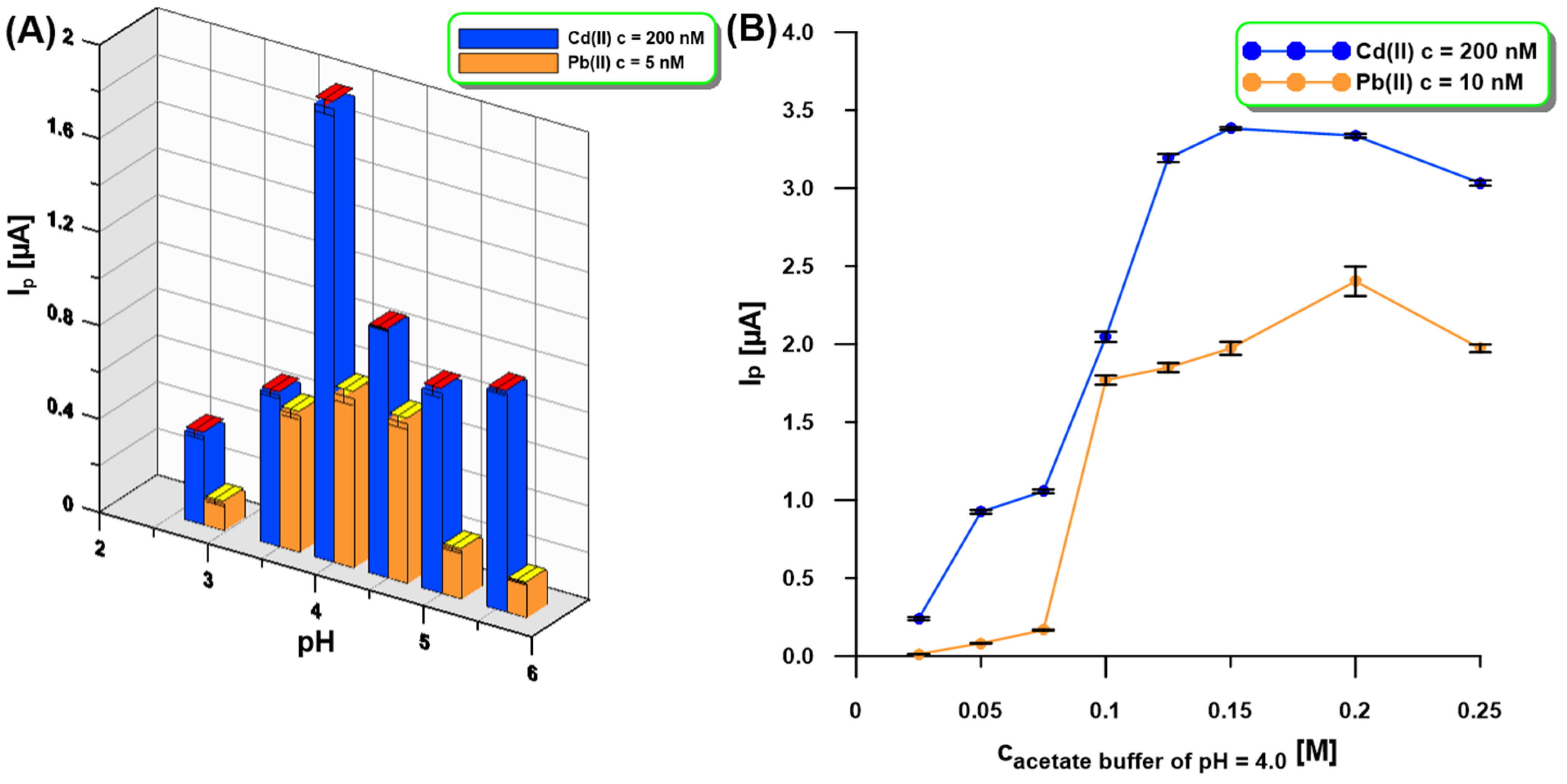
The influence of the supporting electrolyte pH (0.1 M acetic acid, 0.1 M acetate buffer of pH = 3.5, 4.0, 4.5, 5.0, and 5.6) on the SWASV response of Cd(II) (200 nM) and Pb(II) (5 nM) at the aGCE/BiF activated in 0.1 M PBS of pH = 7 was tested (Figure 4A). It was found that pH has an impact on the peak current (Ip) of Cd(II) and Pb(II) because the Ip values increased up to pH = 4.0 and then decreased. The next step was to study the influence of acetate buffer of pH 4.0 in the concentration range of 0.025–0.25 M (Figure 4B). The highest SWASV response of Cd(II) (200 nM) and Pb(II) (10 nM) was obtained in 0.2 M acetate buffer with pH = 4.0 and therefore it was recommended for further studies.
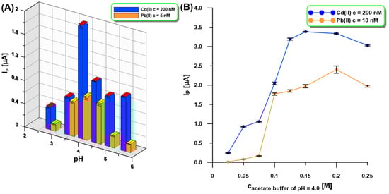
Figure 4.
The influence of pH ((A), 0.1 M acetic acid, 0.1 M acetate buffer of pH = 3.5, 4.0, 4.5, 5.0, and 5.6) and concentration ((B), acetate buffer of pH = 4.0) of the supporting electrolyte on the SWASV response of Cd(II) (200 nM—(A,B)) and Pb(II) (5 nM—(A), 10 nM—(B)). Other SWASV conditions as in Figure 1.
2.3. Bi(III) Concentration and Deposition/Accumulation Studies
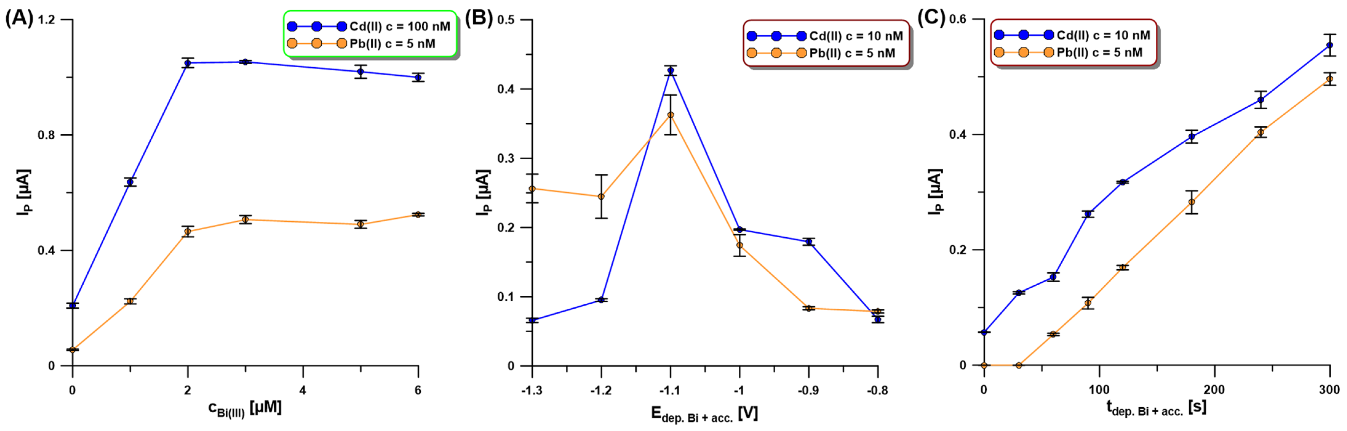
Our SEM studies confirmed that the activation of the electrode in 0.1 M PBS of pH = 7 contributes to a change in the morphology of the deposited bismuth film. Moreover, the Bi(III) concentration as well as the potential and time of simultaneous Bi deposition and Cd and Pb accumulation (Edep.Bi+acc. and tdep.Bi+acc.) influence the morphology of the bismuth film and consequently the Cd and Pb signals. The Bi(III) content in 0.2 M acetate buffer of pH = 4.0 was studied for the Cd(II) and Pb(II) concentrations of 100 nM and 5 nM, respectively (Figure 5A). The current intensity of both cadmium and lead increased with the increase in Bi(III) concentration up to 3.0 µM um and then the signals were practically constant. This is most probably related to the fact that initially the active surface of the electrode increases, i.e., the number of active sites on which Cd and Pb can accumulate increases, but then the active surface is practically constant.
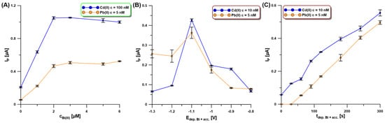
Figure 5.
The influence of Bi(III) concentration (A), Edep.Bi+acc. (B), and tdepBi.+acc. (C) on the SWASV response of Cd(II) (100 nM—(A), and 10 nM—(B,C)) and Pb(II) (5 nM—(A–C)). The SWASV conditions: 0.2 M acetate buffer of pH = 4.0, f of 25 Hz, ESW of 25 mV, and ΔE of 4 mV.
In the next stage of the research, the influence of the potential and time of simultaneous Bi deposition and Cd and Pb accumulation (Edep.Bi+acc. and tdep.Bi+acc.) on the SWASV response of Cd(II) (10 nM) and Pb(II) (5 nM) was examined. The Edep.Bi+acc. was changed from −1.3 to −0.8 V for 120 s of tdep.Bi+acc. (Figure 5B). In the presented figure, it can be seen that the highest signals of both metals were obtained using the accumulation potential of −1.1 V. Then, the tdep.Bi+acc. was changed in the range from 0 to 300 s (Figure 5C). It can be stated that without using bismuth modification, only a slight Cd signal is visible, with no lead signal. Analytical signals of Cd and Pb increase practically linearly with an increasing time of the simultaneous deposition of the bismuth film and accumulation of the analytes. However, due to the shortening of the analysis time itself for further measurements, the time of 120 s was chosen.
2.4. Effect of Technique Parameters
For achieving optimum sensitivity, the SWASV technique was selected and its parameters (the frequency—f, the amplitude—ESW, and the step potential—ΔE) optimized. f was investigated in the range of 8–75 Hz at a constant ESW of 25 mV and ΔE of 4 mV (Figure 6A). The Cd (10 nM) and Pb (5 nM) signals reached extreme values for the f of 25 Hz, so this value was approved for further investigation. In the subsequent step of the experiments, the influence of ESW (25–100 mV) on the SWASV responses of Cd(II) (10 nM) and Pb(II) (5 nM) at the aGCE/BiF was studied (Figure 6B). With the increase in ESW, the SWASV responses of Cd(II) increased, reaching the highest intensity at the ESW of 75 mV. On the other hand, the Pb(II) signal reached its maximum value at the ESW equal to 50 mV. As a compromise between both responses, the ESW value of 50 mV was selected. Then, changes in ΔE (2–8 mV), with an f of 25 Hz and ESW of 50 mV as the selected values, were made to study their influence on the SWASV responses of Cd(II) (10 nM) and Pb(II) (5 nM) (Figure 6C). The Cd peak current increased with an increasing ΔE up to 5 mV, while the Pb peak current increased to a ΔE value of 6 mV. As a compromise between the obtained results, the ΔE equal to 5 mV was chosen for further studies.
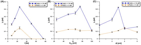
Figure 6.
The influence of f (A), ESW (B), and ΔE (C) on the SWASV response of Cd(II) (10 nM) and Pb(II) (5 nM) at the aGCE/BiF. The SWASV conditions: 0.2 M acetate buffer of pH = 4.0, 3.0 µM Bi(III), electrochemical cleaning of the electrode surface at 0.5 V for 60 s, Edep.Bi+acc. of −1.1 V, and tdep.Bi+acc. of 120 s.
2.5. Electrochemical Cleaning, Calibration, Sensitivity, and Application
Repeatability was evaluated with ten successive SWASV measurements of 10 nM Cd(II) and 5 nM Pb(II) at one aGCE/BiF. The different procedures of electrode surface cleaning between each measurement (0.5 V for 60 s, 1.0 V for 20 s, and 30 times −1.1 V for 1 s and 0.5 V for 1 s) were evaluated. A significant improvement in signal reproducibility was observed for n = 10, when changing potentials were repeated 30 times: −1.1 V for 1 s and 0.5 V for 1 s (RSD for Cd(II): 2.8 vs. 5.7 vs. 1.1%, RSD for Pb(II): 23.8 vs. 10.1 vs. 3.1%). Reproducibility was calculated based on the signals (n = 9) of 10 nM Cd(II) and 5 nM Pb(II) registered at three independently prepared aGCE/BiFs, and RSD values of 5.2% for Cd(II) and 6.3% for the Pb(II) were obtained.
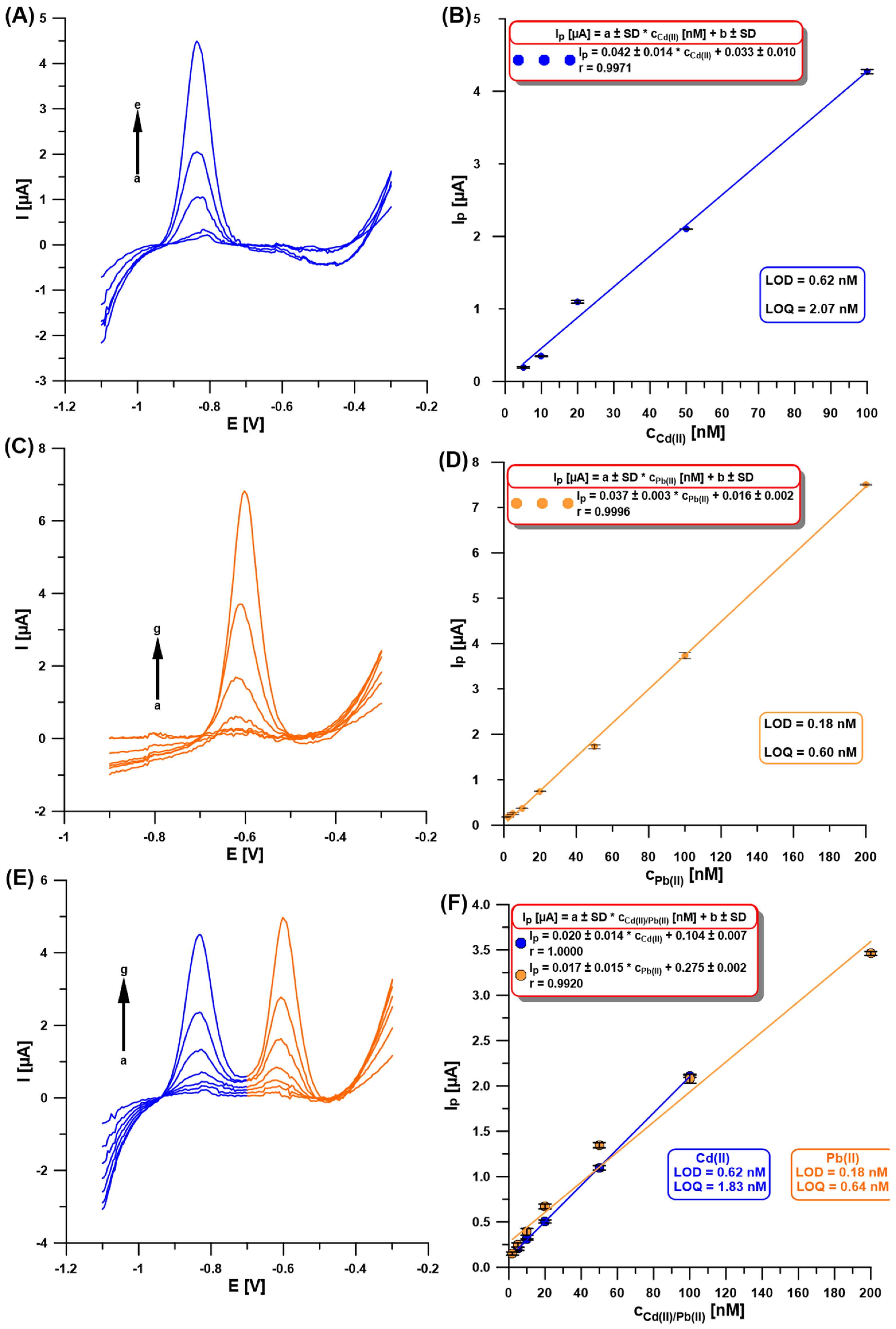
Once the experimental conditions were optimized, the SWASVs for individual Cd(II) and Pb(II), and simultaneous determination of Cd(II) and Pb(II), were recorded (Figure 7A,C,E). As shown in Figure 7B,D,F, the obtained linearity of the calibration curves was very good and extended up to 100 nM for Cd(II) and 200 nM for Pb(II), with the low limits of detection (LOD) and quantification (LOQ) of 0.62 and 0.18 nM, and 2.07 and 0.60 nM, respectively [30]. Table 1 compares the developed procedure for the determination of Cd(II) and Pb(II) using the aGCE/BiF with others described in the literature [9,10,11,12,13,14,15,19,20,21,22,23,24,25,26,27,28]. Without any doubt, it can be stated that the developed procedure offers wide linear ranges of calibration curves and one of the lowest detection and quantification limits for Cd(II) and Pb(II) compared to those described in the literature. In addition, the obtained sensor is environmentally friendly and does not require the use of a wide range of reagents or complicated preparation work.
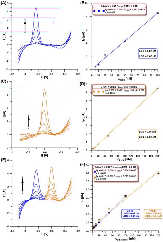
Figure 7.
The SWASVs registered at the aGCE/BiF in 0.2 M acetate buffer of pH = 4.0 containing 0.3 µM Bi(III) and (A) Cd(II) (a → e, 5–100 nM), (C) Pb(II) (a → g, 2–200 nM), (E) Cd(II) and Pb(II) (a → g, 5–100 nM, and 2–200 nM, respectively). The calibration plots of (B) Cd(II), (D) Pb(II), and (F) Cd(II) and Pb(II). The SWASV conditions: the electrochemical cleaning step—changing potentials repeated 30 times (−1.1 V for 1 s and 0.5 V for 1 s), Edep.Bi+acc. of −1.1 V, tdep.Bi+acc. of 120 s, f of 25 Hz, ESW of 50 mV, and ΔE of 5 mV. The baseline was subtracted from each measurement.
The selectivity of the proposed SWASV procedure at the aGCE/BiF was examined by studying the 5 nM Cd(II) and 5 nM Pb(II) responses without and in the presence of metal ions (Fe(III), V(V), Cu(II), Zn(II), Mg(II), Mo(VI), Ni(II), Se(VI), Tl(I), and Co(II)) and Triton X-100 (0.2–2.0 ppm); Triton X-100 added to the supporting electrolyte has a similar influence on the voltammetric response as surfactants in natural waters. It was found that the addition of Triton-X caused a rapid increase in the Cd and Pb signals to over 200% of their original values, which confirms the necessity of pretreatment of water samples, e.g., due to the need for mineralization of the water samples (decomposition of the organic matrix). Moreover, it was found that a 10-fold excess of the tested metal ions does not cause a change in the analytical signals of Cd and Pb of greater than 15% compared to the original values.
To evaluate the capabilities of the proposed methodology for Cd(II) and Pb(II) determination in water samples, the certified reference material (TMRAIN-04, rainwater) was analyzed in triplicate. The obtained results were compared to the certified values, and statistical analysis was performed. Finally, it was found that Δm ≤ UΔ, so there is no significant difference between the measured results and the certified value at a 95% confidence level (coverage factor, k = 2) (Table 2) [31], and therefore the proposed SWASV procedure at the aGCE/BiF can be applied for Cd(II) and Pb(II) analysis of water samples.
Table 2.
CRM (TMRAIN-04) analysis.
Moreover, the developed procedure was applied to the analysis of river water samples, and the determined values of Cd(II) and Pb(II) were 9.50 ± 0.48 nM and 12.27 ± 0.65 nM, respectively. The values of recoveries (samples enriched with 10 nM Cd(II) and Pb(II)) were 107% of Cd(II) and 109% for Pb(II), respectively.
3. Materials and Methods
3.1. Instrumentation
For the electrochemical experiments, a potentiostat/galvanostat (µAutolab, Utrecht, The Netherlands, Eco Chemie) coupled with GPES 4.9 software (voltammetric studies) was used. Commercially available glassy carbon electrodes (geometric area of 3.14 mm2, Mineral, Warsaw, Poland) were polished using 0.3 µm alumina slurry on a Buehler polishing pad (Lake Bluff, IL, USA). The measurements were performed in a three-electrode configuration consisting of the activated glassy carbon electrode with an electrochemically deposited bismuth film (aGCE/BiF, working), a silver chloride electrode (3 M KCl, reference), and a Pt wire (auxiliary electrode). Microscopic images of the GCE/BiF and aGCE/BiF surfaces were obtained using a scanning electron microscope (SEM, high-resolution, Quanta 3D FEG, FEI, Hillsboro, OR, USA). The certified reference materials were mineralized using a UV digester purchased from Mineral, Warsaw, Poland.
3.2. Reagents
The stock standard solutions of Pb(II), Cd(II), and Bi(III) (1 g/L, Merck, Darmstadt, Germany) were dissolved in 0.1 M HNO3 (Merck, Darmstadt, Germany) to the required dilution. A 0.1 M PBS (phosphate-buffered saline) solution of pH = 7 was used for the electrochemical activation of the GCE surface. Non-aerated 0.2 M acetate buffer (pH = 4.0 ± 0.1) was used as a supporting electrolyte (prepared from CH3COOH and NaOH, Merck Merck, Darmstadt, Germany). We prepared 1 mM solutions of Fe(III), V(V), Cu(II), Zn(II), Mg(II), Mo(VI), Ni(II), Se(VI), Tl(I), and Co(II) from reagents bought from Merck in ultra-purified water (>18 MΩ cm, Milli-Q system, Millipore, Gillingham, UK). Moreover, to study the interference effect, a Triton X-100 (Fluka, Gillingham, UK) was used. Certified reference material (CRM), rainwater TMRAIN-04, was obtained from Environment Canada (Burlington, ON, Canada). The CRM and river water (Poland) samples were mineralized by UV irradiation for 3 h. Then, 6.5 mL of the sample was introduced into the electrochemical cell, and the voltammograms were registered.
3.3. GCE Surface Activation and SWASV Measurements
Before the series of SWASV measurements, the GCE surface was pre-anodized in a 0.1 M PBS solution of pH = 7 using five cyclic voltammetric (CV) scans in the potential range of −1.5–2.5 V at a scan rate (ν) of 100 mV/s [18]. Then, the Cd(II) and Pb(II) measurements were performed in 0.2 M acetate buffer (pH = 4) containing 3.0 µM Bi(III). The optimized SWASV parameters were as follows: the electrochemical cleaning step—30 times (−1.1 V) for 1 s and 0.5 V for 1s; simultaneous Bi deposition and Cd and Pb accumulation at −1.1 V (Edep.Bi+acc.) for 120 s (tdep.Bi+acc.); the frequency (f) of 25 Hz; the amplitude (ESW) of 50 mV; and the step potential (ΔE) of 5 mV. The baseline was subtracted from each measurement. The average peak current values are shown with standard deviation (SD) for three measurements.
4. Conclusions
The investigation performed in this study shows the promising role of the activated glassy carbon electrode with an in situ deposited bismuth film (aGCE/BiF) to individually and simultaneously determine the nanotrace levels of Cd(II) and Pb(II) by square-wave anodic stripping voltammetry (SWASV). The results demonstrated that the simple procedure of activation (0.1 M phosphate-buffered saline (PBS) of pH = 7, five cyclic voltammetric scans in the range of −1.5–2.5 V at ν of 100 mV/s) before the series of measurements contributes to changes in the morphology of the deposited bismuth film, increasing the active surface of the electrode and improving the rate of charge transfer between the electrode and the solution. The developed procedure offers wide linear ranges of calibration curves (5–100 nM for Cd(II), and 2–200 nM for Pb(II)) and some of the lowest detection and quantification limits for Cd(II) and Pb(II) (0.62 and 0.18 nM, and 2.07 and 0.60 nM, respectively) compared to those described in the literature. In addition, the obtained sensor is environmentally friendly and does not require the use of a wide range of reagents or complicated preparation work. The newly prepared method was used to determine the amounts of Pb(II) and Cd(II) in the certified reference material, and the results were in agreement with the certified values. Moreover, the procedure was successfully applied to determine Cd(II) and Pb(II) in river samples. The satisfactory accuracy and precision of the SWASV procedure were confirmed in our statistical evaluation.
Author Contributions
Conceptualization, K.T.-R. and A.K.; methodology, K.T.-R. and A.K.; validation, K.T.-R. and A.K.; investigation, K.T.-R. and A.K.; writing—original draft preparation, K.T.-R. and A.K.; writing—review and editing, K.T.-R. and A.K.; visualization, K.T.-R. and A.K.; supervision, K.T.-R. All authors have read and agreed to the published version of the manuscript.
Funding
This research received no external funding.
Institutional Review Board Statement
Not applicable.
Informed Consent Statement
Not applicable.
Data Availability Statement
The original contributions presented in this study are included in the article. Further inquiries can be directed to the corresponding author.
Conflicts of Interest
The authors declare no conflicts of interest.
References
- Mitra, S.; Chakraborty, A.J.; Tareq, A.M.; Emran, T.B.; Nainu, F.; Khusro, A.; Idris, A.M.; Khandaker, M.U.; Osman, H.; Alhumaydhi, F.A.; et al. Impact of heavy metals on the environment and human health: Novel therapeutic insights to counter the toxicity. J. King Saud Univ. Sci. 2022, 34, 101865. [Google Scholar] [CrossRef]
- Manju, M. Effects of heavy metals on human health. Int. J. Res. Granthaalayah 2015, 3, 1–7. [Google Scholar]
- Sall, M.L.; Diaw, A.K.D.; Gningue-Sall, D.; Aaron, S.E.; Aaron, J.-J. Toxic heavy metals: Impact on the environment and human health and treatment with conducting organic polymers, a review. Environ. Sci. Pollut. Res. 2020, 27, 29927–29942. [Google Scholar] [CrossRef]
- Zhang, H.; Reynolds, M. Cadmium exposure in living organisms: A short review. Sci. Total Environ. 2019, 678, 761–767. [Google Scholar] [CrossRef]
- Galal-Gorchev, H. Dietary intake, levels in food and estimated intake of lead, cadmium, and mercury. Food Addit. Contam. 1993, 10, 115–128. [Google Scholar] [CrossRef] [PubMed]
- Oymak, T.; Tokalıoğlu, Ş.; Yılmaz, V.; Kartal, Ş.; Aydın, D. Determination of lead and cadmium in food samples by the coprecipitation method. Food Chem. 2009, 113, 1314–1317. [Google Scholar] [CrossRef]
- Zhang, Z.; Shimbo, S.; Ochi, N.; Eguchi, M.; Watanabe, T.; Moon, C.; Ikeda, M. Determination of lead and cadmium in food and blood by inductively coupled plasma mass spectrometry: A comparison with graphite furnace atomic absorption spectrometry. Sci. Total Environ. 1997, 205, 179–187. [Google Scholar] [CrossRef]
- Alqahtani, A.M.; Mojally, M.; Sayqal, A.; Ainousah, B.E.; Alqmash, A.; Alzahrani, S.; Alqurashi, G.; Wawi, O.; Alsharif, A. Determination of lead and cadmium concentration in cosmetic products in the Saudi market. J. Umm Al-Qura Univ. Appl. Sci. 2024, 10, 146–155. [Google Scholar] [CrossRef]
- Abbasi, S.; Khodarahmiyan, K.; Abbasi, F. Simultaneous determination of ultra trace amounts of lead and cadmium in food samples by adsorptive stripping voltammetry. Food Chem. 2011, 128, 254–257. [Google Scholar] [CrossRef]
- Hu, C.; Wu, K.; Dai, X.; Hu, S. Simultaneous determination of lead(II) and cadmium(II) at a diacetyldioxime modified carbon paste electrode by differential pulse stripping voltammetry. Talanta 2003, 60, 17–24. [Google Scholar] [CrossRef]
- Birara, A.; Washe, A.P.; Bayeh, Y.; Ashebr, T.G. Simultaneous quantification of Cd(II) and Pb(II) by bismuth/poly(bromocresol purple) modified screen-printed carbon-electrode in wastewater. Int. J. Electrochem. Sci. 2024, 19, 100431. [Google Scholar] [CrossRef]
- Yang, D.; Wang, L.; Chen, Z.; Megharaj, M.; Naidu, R. Voltammetric Determination of Lead (II) and Cadmium (II) Using a Bismuth Film Electrode Modified with Mesoporous Silica Nanoparticles. Electrochim. Acta 2014, 132, 223–229. [Google Scholar] [CrossRef]
- Pei, J.; Yu, X.; Zhang, C.; Liu, X. Development of a Boron-Doped Diamond Electrode for the Simultaneous Detection of Cd2+ and Pb2+ in Water. Int. J. Electrochem. Sci. 2019, 14, 3393–3407. [Google Scholar] [CrossRef]
- Lin, H.; Li, M.; Mihailovič, D. Simultaneous Determination of Copper, Lead, and Cadmium Ions at a Mo6S9−xIx Nanowires Modified Glassy Carbon Electrode Using Differential Pulse Anodic Stripping Voltammetry. Electrochim. Acta 2015, 154, 184–189. [Google Scholar] [CrossRef]
- Liu, Y.; Zhang, J.; Du, X.; Cao, Y.; Sun, Y. One-step synthesis of Ag nanoparticles decorated graphene for application in electrochemical detection of Pb2+ and Cd2+ ions. Int. J. Electrochem. Sci. 2021, 16, 210551. [Google Scholar] [CrossRef]
- Tyszczuk-Rotko, K.; Keller, A.; Gorylewski, D.; Kozak, J.; Staniec, K.; Wójciak, M.; Sowa, I. Sensitive and selective antioxidant curcumin analysis using anionic surfactant modified glassy carbon electrode. Microchem. J. 2024, 201, 110697. [Google Scholar] [CrossRef]
- Abdel-Aziz, A.M.; Hassan, H.H.; Badr, I.H.A. Activated Glassy Carbon Electrode as an Electrochemical Sensing Platform for the Determination of 4-Nitrophenol and Dopamine in Real Samples. ACS Omega 2022, 7, 34127–34135. [Google Scholar] [CrossRef]
- Abdel-Aziz, A.M.; Hassan, H.H.; Badr, I.H.A. Glassy carbon electrode electromodification in the presence of organic monomers: Electropolymerization versus activation. Anal. Chem. 2020, 92, 7947–7954. [Google Scholar] [CrossRef]
- De Benedetto, A.; Torre, A.D.; Guascito, M.R.; Di Corato, R.; Chirivì, L.; Rinaldi, R.; Aloisi, A. Spectroscopic investigations of a commercial graphite screen printed electrode modified by bismuth oxide drop deposition and electrochemical reduction, for cadmium and lead ions simultaneous determination. J. Electroanal. Chem. 2024, 964, 118341. [Google Scholar] [CrossRef]
- Albalawi, I.; Hogan, A.; Alatawi, H.; Moore, E. A sensitive electrochemical analysis for cadmium and lead based on Nafion-Bismuth film in a water sample. Sens. Bio-Sens. Res. 2021, 34, 100454. [Google Scholar] [CrossRef]
- Al-Hossainy, A.F.; Abd-Elmageed, A.A.I.; Ibrahim, A.T.A. Synthesis, structural and optical properties of gold nanoparticle-graphene-selenocysteine composite bismuth ultrathin film electrode and its application to Pb(II) and Cd(II) determination. Arab. J. Chem. 2019, 12, 2853–2863. [Google Scholar] [CrossRef]
- Wang, Y.; Wu, X.; Sun, J.; Wang, C.; Zhu, G.; Bai, L.P.; Jiang, Z.H.; Zhang, W. Stripping voltammetric determination of cadmium and lead ions based on a bismuth oxide surface-decorated nanoporous bismuth electrode. Electrochem. Commun. 2022, 136, 107233. [Google Scholar] [CrossRef]
- Wang, J.; Lu, J.; Hocevar, S.B.; Farias, P.A.; Ogorevc, B. Bismuth-coated carbon electrodes for anodic stripping voltammetry. Anal. Chem. 2000, 72, 3218–3222. [Google Scholar] [CrossRef]
- Rojas-Romo, C.; Aliaga, M.E.; Arancibia, V.; Gomez, M. Determination of Pb(II) and Cd(II) via anodic stripping voltammetry using an in-situ bismuth film electrode. Increasing the sensitivity of the method by the presence of Alizarin Red S. Microchem. J. 2020, 159, 105373. [Google Scholar] [CrossRef]
- Nagles, E.; Arancibia, V.; Rtos, R. Determination of Lead and Cadmium in the Presence of Quercetin–5′–sulfonic Acid by Adsorptive Stripping Voltammetry with a Hanging Mercury Drop Electrode and a Nafion–coated Mercury Film Electrode. Int. J. Electrochem. Sci. 2012, 7, 4545–4558. [Google Scholar] [CrossRef]
- Lara, J.; Torres, J.F.; Beltrán, O.G.; Nagles, E.; Hurtado, J. Simultaneous Determination of Lead and Cadmium by Stripping Voltammetry Using in-situ Mercury Film Glassy Carbon Electrode Coated with Nafion-Macrocyclic Ester. Int. J. Electrochem. Sci. 2017, 12, 6920–6929. [Google Scholar] [CrossRef]
- Lima, T.M.; Soares, P.I.; Do Nascimento, L.A.; Franco, D.L.; Pereira, A.C.; Ferreira, L.F. A novel electrochemical sensor for simultaneous determination of cadmium and lead using graphite electrodes modified with poly(p-coumaric acid). Microchem. J. 2021, 168, 106406. [Google Scholar] [CrossRef]
- Antunović, V.; Ilić, M.; Baošić, R.; Jelić, D.; Lolić, A. Synthesis of MnCo2O4 nanoparticles as modifiers for simultaneous determination of Pb(II) and Cd(II). PLoS ONE 2019, 14, e0210904. [Google Scholar] [CrossRef]
- Kozak, J.; Tyszczuk-Rotko, K.; Gorylewski, D. A nanoporous screen-printed carbon sensor for environmental and clinical monitoring of the antibiotic ciprofloxacin. Measurement 2023, 222, 113626. [Google Scholar] [CrossRef]
- Kozak, J.; Tyszczuk-Rotko, K. Screen-printed gold electrode for ultrasensitive voltammetric determination of the antipsychotic drug thioridazine. Measurement 2023, 217, 113107. [Google Scholar] [CrossRef]
- Linsinger, T.P.J. Comparison of Measurements Results with the Certified Value. ERM Application Note 1. July 2005. Available online: https://crm.jrc.ec.europa.eu/ (accessed on 1 February 2025).

Disclaimer/Publisher’s Note: The statements, opinions and data contained in all publications are solely those of the individual author(s) and contributor(s) and not of MDPI and/or the editor(s). MDPI and/or the editor(s) disclaim responsibility for any injury to people or property resulting from any ideas, methods, instructions or products referred to in the content. |
© 2025 by the authors. Licensee MDPI, Basel, Switzerland. This article is an open access article distributed under the terms and conditions of the Creative Commons Attribution (CC BY) license (https://creativecommons.org/licenses/by/4.0/).