Abstract
Photonic chip-based methods for spectroscopy are of considerable interest due to their applicability to compact, low-power devices for the detection of small molecules. Waveguide-enhanced Raman spectroscopy (WERS) has emerged over the past decade as a particularly interesting approach. WERS utilizes the evanescent field of a waveguide to generate Raman scattering from nearby analyte molecules, and then collects the scattered photons back into the waveguide. The large interacting area and strong electromagnetic field provided by the waveguide allow for significant enhancements in Raman signal over conventional approaches. The waveguide can also be coated with a molecular class-selective sorbent material to concentrate the analyte, thus further increasing the Raman signal. This review provides an overview of the historical development of WERS and highlights recent theoretical and experimental achievements with the technique.
1. Introduction
There is an ever-increasing need for rapid yet low-cost detection of small molecules in many fields including point-of-care (POC) clinical diagnostics, environmental and industrial surveillance, and safety monitoring for food and other consumer goods. Sensors, defined here as devices that measure the presence and/or concentration of biological or chemical analytes, are already playing an important role in addressing these needs [1]. Most biosensing techniques with high specificity require covalently attached probes (antibodies, enzymes, DNA/RNA strands, aptamers, etc.) to act as specific biorecognition element for analytes [2,3,4,5]. Both “labeled” immunoassay techniques such as lateral flow assays and novel formats including lab-on-a-chip and label-free biosensors widely employed in POC detection [6] rely on the high affinity of antibodies toward their respective antigens for analyte recognition. However, the use of biopolymeric capture probes is less feasible when the molecular weight of the target analyte is small, in part because of the small binding that surface small molecules present (preventing the use of sandwich antibodies or labeling reagents). For label-free biosensors reliant on refractive index-based changes, small molecules present an additional challenge because they do not perturb the response of the sensor unless at high concentration. In the context of POC diagnostics, the most prominent set of diagnostically relevant molecules is the basic metabolic panel (BMP), which consists of glucose, calcium, sodium, potassium, carbon dioxide, chloride, BUN (blood urea nitrogen), and creatinine. These analytes range in molecular weight from 23 to 113 g/mol. Likewise, many of the analytes of interest industrially and in the context of environmental monitoring are small molecules.
To simplify the detection of small molecules, considerable research effort is being focused on vibrational spectroscopies, including infrared (IR) and Raman spectroscopy, as they directly identify and quantify molecules using vibrational characteristics uniquely determined by their molecular structure. Surface IR spectroscopy with various enhancement mechanisms, mainly attenuated total reflection infrared (ATR-IR) spectroscopy [7,8,9], infrared reflection absorption spectroscopy (IRAS or IRRAS) [10], and surface-enhanced infrared spectroscopy (SEIRAS) [8,9], have been used in the biosensing of small molecules [11]. However, since biological samples of interest are usually aqueous, IR spectroscopies suffer from the strong absorption of water over their mid-infrared (MIR, ~2–16 μm) operating wavelength (Figure 1). It is for this reason that Raman spectroscopy provides distinct advantages.
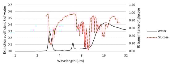
Figure 1.
Extinction coefficient of water superimposed on the infrared spectrum of glucose (using data adapted from [12,13]). Water strongly absorbs at wavelengths corresponding to several of the characteristic bands of glucose, hindering its observation in aqueous samples by infrared spectroscopy.
Raman spectroscopy detects the inelastic Raman scattering of incident photons by analyte molecules [14]. The inelastically scattered photons have a wavelength shift (also known as a Stokes shift) from the wavelength of the incident photons, which is a function of the vibrational energies of the molecule undergoing analysis. By choosing an appropriate original wavelength of incident light (typically described as the “pump wavelength”), the scattered Raman signal can avoid the strong absorption wavelength range of water or other substrates. While this provides a distinct advantage over absorption spectroscopy, Raman spectroscopy also has a significant disadvantage in that Raman scattering is intrinsically very weak. For example, Rohleder et al. compared mid-IR and Raman spectroscopy in the quantitative analysis of serum and found that similar accuracy was achievable with both techniques, but the measurement time needed for Raman spectroscopy was 10 times longer (5 min) than for mid-IR spectroscopy (30 s) [15]. To address this problem, efforts have been made to enhance the scattering. Surface-enhanced Raman scattering (SERS) uses metal (mostly silver and gold) nanostructured substrates to locally enhance Raman scattering from analyte molecules by factors up to 106–1010 [16,17]. Despite many successful applications of SERS in biosensing [16,18,19] the reproducibility and robustness of the substrate are continuing concerns [17,20]. Moreover, SERS requires the analyte molecules to fall in optimally enhancing “hotspots” around the metal nanostructures, which may be difficult and inefficient when the analyte concentration is low and can also further increase the inconsistency of the detection. The hotspots may also get blocked by non-analyte molecules in complex samples [14].
WERS is an alternative, recently emerging [21] approach to enhancing the sensitivity of Raman that does not rely on metal nanostructures, thereby avoiding the challenges of SERS discussed above. WERS relies on the interaction of analytes with the evanescent field of a waveguide (discussed below) on a photonic chip. In contrast to SERS, where Raman scattering only comes from the enhancing hotspots, in WERS, analytes can interact with the evanescent field over the entire length of the waveguide, and the waveguide also collects and conducts the Raman scattering to the spectrometer. In theory, waveguides provide dozens-fold enhancement of Raman signal per cm [22]. For example, a direct experimental comparison of WERS with a standard confocal Raman microscope reported by Dhakal et al. [23] achieved more than four-orders-of-magnitude higher spontaneous Raman signal for WERS. As we discussed below, different configurations and the use of polymer sorbents can provide enhancements well beyond these levels (up to 108). The manufacture of waveguides for integrated photonics applications is mature and continuously improving because it relies on the same processes used in the microelectronics industry [24]. Waveguide structures can be produced with high consistency, avoiding the manufacturing scalability concerns that remain a challenge with SERS. Of course, as a label-free spectroscopic technique, there is also no need for perishable and expensive labels or probes.
WERS Basics
A dielectric optical waveguide is a structure that conducts electromagnetic waves, i.e., light. Waveguides constrain light and allow it to propagate along a “core” with higher refractive index compared to surrounding “cladding”, via total internal reflection. For example, an optical fiber is a type of waveguide. In this case, the core is glass (silica) or a polymer, and the cladding is either a polymer with a lower refractive index than the core or air. Figure 2 shows some common types of optical waveguides. Waveguides are useful in sensing in large part because the electromagnetic field of light conducted along the waveguide is not totally confined in the core region. It extends into the cladding, producing what is called an evanescent field. Light can interact with molecules falling in the evanescent field and cause Raman scattering. Early experiments with WERS used the electromagnetic field in the core, whereas the majority of recent efforts make use of the evanescent field for sensing. Our discussion of the development of WERS covers both cases but emphasizes the latter.
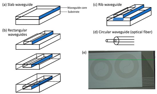
Figure 2.
(a–d), adapted from [25]) Basic waveguide structures: slab waveguide, rectangular (channel/strip/wire) waveguide, and circular waveguide (optical fiber). Slot waveguides, not shown in this figure, consist of two rectangular waveguides positioned closely together in parallel. (e) Laser confocal microscope image of a WERS chip with spiral waveguides. The green line is a horizontal imaging reference.
2. Historical Development of WERS
As mentioned above, WERS was first demonstrated with liquid-core waveguides [26]. In an early report, a 10 to 25 m hollow fused quartz optical fiber with core diameter of ~75 μm was filled with benzene (C6H6) or tetrachloroethylene (C2Cl4) as the analyte. The waveguide conducted the pump laser and collected the Raman signal from the analyte core. Compared to conventional Raman spectroscopy, this technique enhanced the signal by factors of 102 to 103.
While such early experiments using optical fibers for WERS were impressive, implementation of the technique in a chip-based format paved the way for compact, low-cost sensing systems with significant advantages of size, weight, and power (SWAP) typical of integrated photonics [27]. A key demonstration of WERS by Levy in 1974 used a slab waveguide consisting of the analyte itself [28]. Methyl methacrylate (MMA) was made into a film a few μm thick and served as the core, both conducting the pump laser light and collecting the Raman signal of the material. Five years later, Rabolt [29] pushed the thickness of analyte thin film to as small as 1 μm without apparent background Raman from the substrate holding the film. These efforts demonstrated the feasibility of WERS, but also highlight the need to minimize Raman signals from the waveguide itself if one wants to detect an analyte external to the waveguide.
As a next step up in complexity from the analyte-core waveguides described above, Rabolt et al. [30] tested waveguides with a two-layer core. Two films together served as the core: one film was a thicker, known material with a well-characterized Raman spectrum, while the other film was only a few nm thick and actually the analyte to be tested. In this way, the analyte could be a molecular monolayer, and this Raman signal reflects the information about the bonds between the analyte and the thicker layer. In some ways, the analyte in this implementation effectively straddles the core and evanescent regions of the waveguide.
Similarly structured waveguides were used to measure the Raman signal of 8 nm polystyrene, a monolayer of the protein bovine albumin and dimyristoyl phosphatidylethanolamine (DMPE) Langmuir–Blodgett monolayers [31]. The substrate, core, and cladding were SiO2, ZnO, and air, respectively. The analyte was a thin film directly on the top of the ZnO core; however, here, it was considered to be located in the evanescent field instead of serving as a part of the core. The ZnO has higher refractive index than the polymer and biological analytes; thus, the local electric field intensity is higher and better enhances the Raman scattering. That is the reason why using a high-refractive-index core and exciting the analyte with the evanescent field became the mainstream of WERS. However, since the core is also exposed to the electromagnetic field, a potential disadvantage of this approach is that its emission will also be collected. Here, two peaks in the Raman spectrum of the ZnO core obscure the weak signal from analyte around their wavelength range. This result highlighted the need to optimize the material of the core to prevent core Raman signals from interfering with analyte signals.
For the example discussed above, Raman signals were collected using a lens positioned above the waveguide rather than at the waveguide end, as would be required for a fully integrated solution. In a follow-up to their work with ZnO core waveguides, the Greve group tested Si3N4 under the hypothesis that this would produce significantly less background as a core material than ZnO [32]. Here, the measurement geometry was also changed; this time they collected the Raman signal from the waveguide output. It was previously demonstrated both experimentally [33] and theoretically [34] by O’Connor and Tauc that Raman scattering excited by the evanescent field in the waveguide cladding can couple back to the guided mode. Although the original purpose of this finding was to bring notice to the fact that the optical fibers used in Raman spectroscopy generate background from the fiber’s core and cladding, it also laid the groundwork for later WERS studies using the evanescent field for sensing.
As hypothesized, Greve and colleagues found Si3N4 to have favorable characteristics for waveguide-based Raman measurements. This waveguide material has become the most commonly used waveguide materials for WERS, given its good collection efficiency and low background [35]. It is also convenient because of parallel developments in photonic integrated circuits (PICs) and in the computer industry. Complementary metal–oxide–semiconductor (CMOS) is a type of transistor which is critical for constructing electronic integrated circuit chips such as microprocessors and memory chips. Increasing the density of CMOS gives the chips higher computing power or bigger storage capacity. For years, Moore’s law has successfully predicted that technology developments in the industry would drive a doubling in the number of transistors on an electronic chip every 12–24 months. However, transistor scaling has reached a critical size limit due to electron leakage [36]. Thermal management has also become increasingly challenging as the density of electronic circuitry on computer chips has increased. Photonic circuits have the potential to overcome the bottlenecks imposed on electronic integrated circuits and continue pushing the boundaries of Moore’s law [37]. The fabrication process of photonic circuits can be executed with the CMOS fabricating techniques [38]. This CMOS compatibility is a key driver for the growth of PICs in other areas, including sensing.
Silicon-on-insulator (SOI) and silicon nitride (SiN) are the two most common materials used in the production of PICs, and they are compatible with standard CMOS fabrication methods [39]. As such, there is a large manufacturing infrastructure developed by the microelectronics industry that can be leveraged for PIC production. Standard SOI and SiN platforms are typically around 200–220 nm thick, although significant customization is possible. This design convention for waveguides can be tailored according to the specific needs of the application. Compared to SiN, SOI is theoretically usable but much less preferred for WERS due to silicon’s strong absorption at wavelengths typically used for WERS [23]. The intensity of Raman scattering is proportional to the fourth power of the excitation frequency [40]; hence, the wavelength chosen for the pump laser is as short as possible to maximize the intrinsically small Raman signal. This must be balanced against the fluorescence and absorption of the waveguide material, which increase at shorter wavelengths. Comparing the absorption coefficients of SiN (only showing Si3N4 here) and silicon (Figure 3), SiN has a significant advantage in this regard. However, the fluorescence/luminescence of SiN waveguides can be a problem; therefore, it is important to understand what contributes to the background luminescence of Si3N4 waveguides and how this can be reduced. Dhakal et al. [41] reported that SiN luminescence originates primarily from two sources: the narrow-band peak component is from impurities, especially hydrogen-based compounds and interstitial nitrogen, while the broad-band slowly varying component is from thermal fluctuations of the refractive index and momentum selection rule breaking in the amorphous material. For the slowly varying component, the authors suggested that, if the material is more crystalline, the background spectrum may contract to narrower wavenumber ranges. Those findings remind us to pay attention to the details of waveguide fabrication, such as choosing appropriate chemical vapor deposition and annealing methods. Continued development of manufacturing processes have allowed both loss and luminescence in silicon nitride waveguides to be reduced to manageable levels [42].
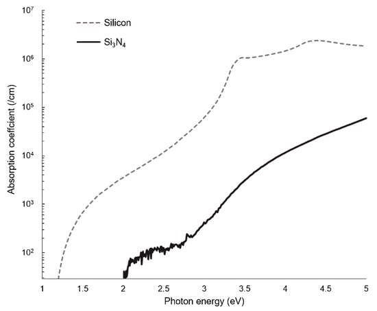
Figure 3.
Absorption coefficient for Si3N4 and silicon as function of incident photon energy (E = hc/λ, where h is Planck’s constant, c is the speed of light, and λ is the wavelength; the x-axis is equivalent to 1240–250 nm; using data adapted from [43,44]).
3. WERS Theory for Rectangular/Channel/Strip/Wire Waveguides
The enhancement factor of WERS versus conventional Raman spectroscopy has been calculated as early as in the first WERS paper by Levy et al. [28]. However, these calculations focused on WERS using the field in the core, instead of the evanescent field in the cladding to generate Raman scattering. With further development of WERS for general-purpose chemical and biological sensing, the most common design is one in which the analyte molecules are located in the evanescent field outside the waveguide, which makes the calculation much less straightforward.
To assess the theoretical performance of WERS for biosensing, Jun et al. [45], Dhakal et al. [46], and Stievater et al. [22] first developed a theoretical framework for the excitation, collection, and enhancement of Raman signal with Si3N4 waveguides, before testing the theory experimentally. The emitting molecule is modeled as an oscillating dipole near the waveguide surface. In the discussion below, we present the key aspect of WERS theory, drawing from [22,45,46].
Collection efficiency:
In the weak coupling regime, the spontaneous emitting rate of a dipolar (analyte) molecule can be calculated using Fermi’s golden rule [45].
where is the dipole position, is the coupling strength between the dipole and the waveguide mode (expressed as electromagnetic field E), and is the density of states (DOS).
For a single-mode rectangular waveguide, we can assume a 1-D DOS due to single-polarization operation. Since we only consider propagation in one direction (i.e., from source to detector along the waveguide), the 1-D DOS should be divided by 2:
where is a unit length and will be canceled out later.
Assuming the dipole is oriented parallel to the electric field, the coupling strength term in Equation (1) is given by the following [45]:
where is the dipole. The normalization factor α is given by the following [45]:
The effective mode volume is defined as follows [45]:
where is the same unit length as in Equation (2). Lastly, the effective mode area at the dipole position is the following [45]:
Equations (1)–(6) describe the spontaneous emitting rate . However, since the emitted light decays in all directions including as it approaches the waveguide, the decay rate also needs to be considered. According to Novotny and Hecht [47] and Jun [45], the decay rate in the background medium is
Plugging Equations (1)–(7) together, the effective Raman cross-section (collection efficiency), which is the portion of the emission power that can be collected into the waveguide, is
Excitation efficiency and overall efficiency:
Power radiated by the dipole in free space is expressed as follows [46]:
where
This describes the excitation of the dipole by the evanescent field. Plugging Equations (9) and (10) into Equation (8), the overall efficiency combining both excitation and emission can be calculated.
Coupling efficiency and waveguide length:
In reality, coupling of the pump laser light into the waveguide and the Raman signal out of the waveguide are not perfect. To take these coupling losses into account, and need to be modified by efficiency terms and , where is the laser power and is the collected Raman power. Therefore, for unit length and a single dipole as the analyte molecule,
In addition to coupling efficiency, there is also a loss during light traveling along the waveguide. Longer waveguides provide a larger contacting area with analyte molecules but suffer more from propagation loss. Modifying Equation (11) with the effect by waveguide length, the final efficiency becomes the following [46]:
where is the molecule density, is waveguide length, and are the propagation losses at the pump wavelength and at the Stokes wavelength, respectively, and .
4. Experimental Verification of WERS Theory
Equation (12) was verified by Dhakal et al. [46] using rectangular Si3N4 waveguides with different lengths. Although the results obtained were found to have a significant standard deviation, the experimental data were consistent with the equation. Likewise, work from the Stievater lab demonstrated good correlation between theory and experiment, but also some variability due to variation in waveguide fabrication and other factors [22]. Later, Dhakal et al. [48] validated the equation for both TE and TM mode using waveguides with different lengths, widths, designs (rectangular and slot waveguides), and refractive indices (Si3N4, TiO2, and silicon). According to their results, for rectangular Si3N4 waveguides, the fundamental quasi-TM mode has an efficiency nearly 2.5 times larger than the quasi-TE mode, and this difference gets larger for waveguides with higher refractive indices. The quasi-TE mode of slot waveguide can achieve even larger efficiency than both TE and TM for a rectangular waveguide. These findings provide direction for researchers seeking to improve their waveguide design for WERS.
5. Raman Emission Collected at the End of Waveguide vs. at the Surface of Waveguide
The theory developed above is focused on collecting Raman signals at the end of a waveguide. As seen in our discussion of early WERS experiments with slab waveguides, collecting from the top surface is also a possibility, and this has the advantage of not needing careful coupling of light from the waveguide into an optical fiber or microscope lens. To test the relative efficiencies of these two methods, Wang et al. [49] compared the collection of Raman emission from the waveguide end and the surface with a 110 nm Ta2O5 slab waveguide. Because of the geometry of the slab, the pump light was chosen to be in TM mode. The dipole under the electric field, therefore, oscillates perpendicular to the waveguide surface. In this case, they calculated that 76.3% of the Raman emission from a dipole will couple into the waveguide. For the remaining proportion, if a coverslip is put above the waveguide to reflect some of the escaping light back into the waveguide, the light coupled will increase by 17.8%. Moreover, collecting at the end accumulates the Raman signal from the analyte molecules all along the waveguide, whereas collecting at the surface only covers a relatively small area. Thus, for better enhancement, the collection site should be at the end, assuming that the propagation loss and coupling loss are not so large as to cancel the benefit. Rectangular waveguides have a substantially smaller top surface area than slab waveguides, which have a width considered to be infinite relative to the wavelength of light. As such, the mode profile of a rectangular waveguide is more similar to that of an optical fiber, making the coupling at the end of the waveguide more efficient.
6. Silicon Nitride and Other Materials for WERS Sensing
Having discussed the early history of and theory behind WERS, we now turn to examples of where Si3N4 WERS has been put to use. Tyndall et al. [50] used WERS with Si3N4 rib waveguides to measure the trace concentrations of four vapor-phase chemical warfare agent simulants: dimethyl methylphosphonate (DMMP), diethyl methylphosphonate (DEMP), trimethyl phosphate (TMP), and triethyl phosphate (TEP). The waveguide core was as thin as 110 nm (compared to a 175 nm core waveguide studied for TE mode) and etched by 55 nm to create the rib structure. A carbosilane sorbent polymer which absorbs the four analyte molecules was deposited on top of the waveguide. This hyperbranched hydrogen bond acidic polymer semi-selectively binds and concentrates the hydrogen bond basic analytes to enhance their Raman signal. The polymer’s background spectrum was taken to make sure it did not have Raman or fluorescence peak interfering with the analytes’ peaks. The thin core was found to decrease the core background and increase the overlap of the quasi-TM mode with the sorbent cladding, improving the signal-to-noise ratio. Figure 4 shows that the height of the Raman peak from the analyte is proportional to the concentration, suggesting that the technique can be made at least semi-quantitative.
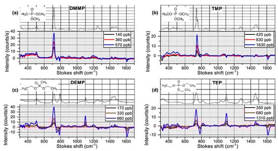
Figure 4.
(Reprinted with permission from [50] © Optica) Background-subtracted WERS spectra of (a) DMMP, (b) TMP, (c) DEMP, and (d) TEP at different concentrations compared to their reference Raman spectra.
In this example, the sorbent layer was key to reaching a low limit of detection. The idea of using solid-phase absorbents to preconcentrate the analyte, thus increasing its Raman signal, was first raised in 1997 by Ewing et al. [51]. The development of analyte class-selective sorbents remains a significant opportunity for extending the capabilities of WERS. In addition to capturing and concentrating analytes of interest, sorbent polymers can provide spectral simplification of a complex mixture by rejecting molecules outside the structural class for which they are designed. The physical barrier provided by a sorbent may prove to be particularly important in whole-blood analysis; hemoglobin present in red blood cells, as well as other blood pigments, produces a large background fluorescence signal that is a well-known complication of Raman measurements in blood [52]. As a guide to evaluating polymer sorbents for WERS, Tyndall et al. described an experimental framework, including figures of merit [53].
For WERS PICs to be useful outside of specialized research laboratories, they must be packaged with optical fibers for light I/O and with microfluidics for sample delivery. Kita et al. [54] reported a packaged and fiber-bonded WERS chip. The coupling fibers were aligned and glued to the chip, and the flow cell for analyte sample was then secured above (Figure 5). A notable feature of the experimental design of this work is that data were collected in a back-reflection Raman signal, allowing the signal to be separated from the forward-propagating pump and waveguide background.
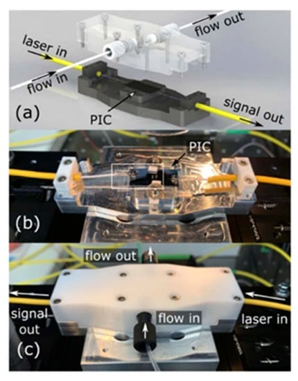
Figure 5.
(Reprinted with permission from [54] © Optica) Fiber-packaged, microfluidic-coupled WERS. (a) Rendering of the assembly with optical fibers affixed to the chip and a flow cell that lowers onto the chip surface. (b) Photograph of the packaged chip with fibers glued to the edge. (c) The packaged chip with the flow cell secured on the top.
Liu et al. [55] demonstrated a WERS sensor incorporating a Si3N4 slot waveguide for detection of low-concentration organic pollutants in water. Mesoporous silica modified by hexamethyldisilazane (HMDS) was used as top cladding to absorb and enrich pollutants in the aqueous sample by 600-fold, which further enhanced the sensitivity of the device. Figure 6 shows the sensor simultaneously quantifying multiple analytes. After measurement, the analyte could be desorbed in 3 min by putting the sensor in pure water. This regeneration ability makes the sensor reusable and reduces the cost.
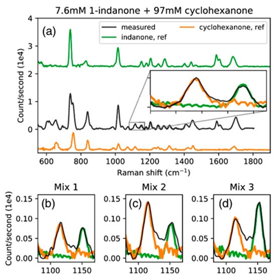
Figure 6.
(Reprinted with permission from [55] © Optica) Background-subtracted spectrum of (a) 7.6 mM (1 g/L) 1-indanone and 97 mM (1%) cyclohexanone solution, (b) 1.9 mM (0.25 g/L) 1-indanone and 24 mM (0.25%) cyclohexanone, (c) 1.9 mM 1-indanone and 48 mM (0.5%) cyclohexanone, and (d) 3.8 mM (0.5 g/L) 1-indanone and 24 mM cyclohexanone.
In addition to Si3N4, Ta2O5 has been studied as a material for the waveguide core. Due to its high refractive index contrast with SiO2, Ta2O5 waveguides confines the mode more tightly than Si3N4 does, enabling the development of more compact photonic circuits with smaller bending radii. Another advantage is that the pumping laser wavelength for Ta2O5 waveguides is in the visible range, making alignment easier and safer. Of course, these advantages must be balanced against the fact that the manufacturing infrastructure for Ta2O5 is much less developed than that for silicon nitride.
Coucheron et al. [56] presented a WERS sensor based on a Ta2O5 slab waveguide for blood analysis. They chose 532 nm as the pump laser wavelength to measure the resonance Raman signal from hemoglobin. Resonance Raman typically focuses only on detection of a single analyte, since the photon energy of the pump laser needs to match the electronic absorption band of the analyte. The authors began with a 15.5 mM solution of hemoglobin in distilled water, allowing the solution to dry on the waveguide measurement. Of course, blood is a highly complex matrix, and significant work remains to demonstrate routine, quantitative detection of analytes in blood using WERS. However, this work constitutes a “foot in the door” for WERS in the field of blood testing.
Ta2O5 also may be combined with glass to make composite optical waveguides. Hu and Qi [57] used such a waveguide for a sensor with a mixed concept of SERS and WERS to overcome the reproducibility challenges often seen with SERS. A 10 nm thick copper phthalocyanine (CuPc) film, used as both the cladding and the analyte, was deposited on the waveguide surface. A solution of NaCl was flowed over the film to increase the refractive index, such that the mode shifts toward the cladding and the electromagnetic field intensity at the CuPc film increases. This effect enhances not only the Raman signal from the film but also the absorption of the pump light by the film. This double enhancement provided an eightfold enhancement of the Raman signal in TM mode. The authors suggested that this approach could be a useful method for monolayer and biomembrane analysis.
As mentioned previously, the waveguide core material needs to have low absorption and emission at the pump wavelength and over the spectral range of Raman signal from analytes of interest. Meanwhile, the refractive index of the core material affects the mode distribution; more specifically, it determines the fraction of the electromagnetic field that can be evanescent and interact with analytes. Raza et al. [58] made a comparison of Al2O3, Si3N4, Ta2O5, and TiO2, which are suitable as the core for WERS considering their high transparency through near-IR wavelengths and the ability to conduct high-intensity laser light. They found that, because of high refractive index contrast versus the cladding, TiO2 (n = 2.33) had the best signal collection efficiency. Si3N4 (n = 1.89) and Ta2O5 (n = 2.11) had comparable collection efficiency, and Al2O3 (n = 1.60) had the worst efficiency among the four materials. However, Al2O3 had the lowest background emission, whereas TiO2 had the highest, eight times higher than Si3N4 and Ta2O5. After balancing the signal collection efficiency and the background, the authors believed Si3N4 and Ta2O5 stood out, but the more highly mature fabrication capabilities for Si3N4 led to a lower waveguide loss, thus representing the current optimum choice.
In addition to these four common materials, Makela et al. [59] used aluminum nitride (AlN) waveguides fabricated with a CMOS-compatible process for WERS. They chose AIN because it has a suitable refractive index (n = 2.1), and the background can be an order of magnitude lower than silicon nitride in the visible regime. Since Raman intensity is proportional to the fourth power of the excitation frequency, using a pump laser of visible light instead of IR increases the Raman signal. The 550 nm thick slab AlN waveguide was fabricated on a 3 μm thick SiO2 undercladding. A 635 nm pump laser was butt-coupled into the waveguide in TM mode. Analyte solution was dropped on the surface, and the Raman signal was collected above the waveguide. Although collecting from above is not as efficient as collecting at the end of waveguide (as discussed above), the authors were able to detect benzene derivatives (toluene and anisole) in benzene as a proof of concept.
Lastly, using a composite core material, an intriguing combination of WERS and SERS was described by the Baets group [60,61]. They covered Si3N4 slot waveguides first with Al2O3 to narrow the slot, and then with Au to serve as an extended enhancing hotspot (Figure 7). Although the Raman signal intensity detected by this setup is weaker compared to conventional SERS, it generates a lower background and, thus, provides a similar signal-to-noise ratio to conventional SERS [58]. The substrate of waveguide-based SERS, i.e., the covered waveguide, is reproducible and consistent. Given that the Raman signal is collected from a waveguide, this implementation is convenient for lab-on-a-chip applications.
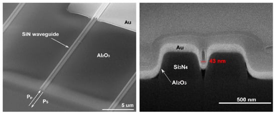
Figure 7.
(Reprinted with permission from [61] © Optica) Waveguide-based nanoplasmonic slot waveguide top view and cross-section.
7. Summary
While still at a relatively early stage as a field of research, WERS is already demonstrating its utility as a sensing approach. By allowing for excitation of analyte molecules along an entire wavelength (which may reach 10’s of cm in a total area <1 cm2), WERS provides significant sensitivity enhancements relative to the intrinsically low signals of “standard” Raman spectroscopy. The evanescent field can be optimized by waveguide geometry to increase the intensity and by refractive index contrast to increase its overlap with analyte. The escaped Raman emission can even be reflected back to the waveguide with additional components such as a coverslip or the boundary of cladding layer. The ability to further enhance detection capability via the use of sorbent coatings, which may be analyte class-selective in addition to providing concentration enhancement, is a further advantage. Lastly, the small footprint and compatibility with CMOS fabrication of WERS are attractive characteristics.
Waveguide loss and background represent two significant technical challenges to WERS. Losses include propagation loss and coupling loss. Bends and imperfections in waveguide fabrication such as rough walls contribute to the propagation loss and can be improved by design and fabrication techniques. Coupling loss can be minimized by matching the mode profile between the waveguide and the other optical component, which is usually an optical fiber or a lens. Edge couplers have been intensively studied for this purpose [62]. The background is determined by the waveguide material. During design, researchers should select the waveguide material whose emission peaks are far away from the Raman signal of analytes. During fabrication, appropriate procedures also lower the background by reducing the impurity and amorphism. Recent results from various foundries indicate that the loss and background challenges can be overcome. The performance of the waveguide can also be affected by the environment. For example, the refractive index of Si3N4 is temperature-dependent [63]. This requires either that the WERS setup sits in a room with a constant temperature or controlling module, or that it gets calibrated prior to use.
Of course, integration of additional components of a WERS system (source, filters, waveguides, and spectrometer) may be considered. For example, Tyndall et al. [64] demonstrated the successful integration of an on-chip filter for WERS to get rid of the pump laser before spectrum collection. The cascaded Mach–Zehnder interferometer lattice filter blocked 75% of the power at the notch wavelength and maintained >90% transmission for wavelengths outside the filter notch. Considerable insight is also being gained into on-chip sources and spectrometers, although this is outside the scope of this manuscript. In addition to filters, rapid advances in the integrated photonics field are allowing for the integration of light sources and other even more complicated components on chips together with the waveguides. These developments give WERS a bright future in sensing.
Author Contributions
Writing—original draft preparation, P.W. and B.L.M.; writing—review and editing, P.W. and B.L.M.; funding acquisition, B.L.M. All authors have read and agreed to the published version of the manuscript.
Funding
This research was funded by the Department of Commerce Rapid Assistance for Coronavirus Economic Response (RACER) program, as administered by NIST (contract 70NANB22H015), and by the US Army, via contract W911SR-20-C-0010. The views and opinions expressed in this paper are those of the authors and do not reflect the official policy or position of the United States Army, the Department of Defense, or the US Government.
Conflicts of Interest
The authors declare no conflict of interest.
List of Abbreviations
| AlN | Aluminum nitride |
| ATR-IR Spectroscopy | Attenuated total reflection infrared spectroscopy |
| BMP | Basic metabolic panel |
| BUN | Blood urea nitrogen |
| CMOS | Complementary metal–oxide–semiconductor |
| CuPc | Copper phthalocyanine |
| DEMP | Diethyl methylphosphonate |
| DMMP | Dimethyl methylphosphonate |
| DMPE | Dimyristoylphosphatidylethanolamine |
| DOS | Density of states |
| HMDS | Hexamethyldisilazane |
| IR | Infrared |
| IRAS or IRRAS | Infrared reflection absorption spectroscopy |
| MIR | Mid-infrared |
| MMA | Methyl methacrylate |
| PICs | Photonic integrated circuits |
| POC | Point-of-care |
| SEIRAS | Surface-enhanced infrared spectroscopy |
| SERS | Surface-enhanced raman scattering |
| SiN | Silicon nitride |
| SOI | Silicon-on-insulator |
| SWAP | Size, weight, and power |
| TEP | Triethyl phosphate |
| TMP | Trimethyl phosphate |
| WERS | Waveguide-enhanced raman spectroscopy |
References
- Rinken, T. State of the Art in Biosensors: Environmental and Medical Applications; Intech Open: London, UK, 2013. [Google Scholar]
- Zhang, W.; Guo, S.; Carvalho, W.S.P.; Jiang, Y.; Serpe, M.J. Portable point-of-care diagnostic devices. Anal. Methods 2016, 8, 7847–7867. [Google Scholar] [CrossRef]
- Liu, J.; Geng, Z.; Fan, Z.; Liu, J.; Chen, H. Point-of-care testing based on smartphone: The current state-of-the-art (2017–2018). Biosens. Bioelectron. 2016, 132, 17–37. [Google Scholar] [CrossRef] [PubMed]
- Prante, M.; Segal, E.; Scheper, T.; Bahnemann, J.; Walter, J. Aptasensors for point-of-care detection of small molecules. Biosensors 2020, 10, 108. [Google Scholar] [CrossRef] [PubMed]
- Chen, S.Y.; Li, Z.; Li, K.; Yu, X.Q. Small molecular fluorescent probes for the detection of lead, cadmium and mercury ions. Coord. Chem. Rev. 2021, 429, 213691. [Google Scholar] [CrossRef]
- Vashist, S.K.; Luong, J.H. Immunoassays: An overview. In Handbook of Immunoassay Technologies; Vashist, S.K., Luong, J.H., Eds.; Academic Press: Cambridge, MA, USA, 2018; pp. 1–18. [Google Scholar]
- Chittur, K.K. FTIR/ATR for protein adsorption to biomaterial surfaces. Biomaterials 1998, 19, 357–369. [Google Scholar] [CrossRef]
- Sun, H.; Sun, C.; Ding, X.; Lu, H.; Liu, M.; Zhao, G. In situ monitoring of the selective adsorption mechanism of small environmental pollutant molecules on aptasensor interface by attenuated total reflection surface enhanced infrared absorption spectroscopy (ATR–SEIRAS). J. Hazard. Mater. 2021, 403, 123953. [Google Scholar] [CrossRef] [PubMed]
- Hu, Y.; Chen, Q.; Ci, L.; Cao, K.; Mizaikoff, B. Surface-enhanced infrared attenuated total reflection spectroscopy via carbon nanodots for small molecules in aqueous solution. Anal. Bioanal. Chem. 2019, 411, 1863–1871. [Google Scholar] [CrossRef]
- Hoffmann, F.M. Infrared reflection-absorption spectroscopy of adsorbed molecules. Surf. Sci. Rep. 1983, 3, 107–192. [Google Scholar] [CrossRef]
- Boujday, S.; Lamy de la Chapelle, M.; Srajer, J.; Knoll, W. Enhanced vibrational spectroscopies as tools for small molecule biosensing. Sensors 2015, 15, 21239–21264. [Google Scholar] [CrossRef]
- Hale, G.M.; Querry, M.R. Optical constants of water in the 200-nm to 200-μm wavelength region. Appl. Opt. 1973, 12, 555–563. [Google Scholar] [CrossRef]
- D-Glucose Infrared Spectrum. Available online: https://webbook.nist.gov/cgi/inchi?ID=C2280446&Type=IR-SPEC&Index=1#IR-SPEC (accessed on 22 September 2022).
- Smith, E.; Dent, G. Modern Raman Spectroscopy: A Practical Approach; John Wiley & Sons: Hoboken, NJ, USA, 2019; p. 16. [Google Scholar]
- Rohleder, D.R.; Kocherscheidt, G.; Gerber, K.; Kiefer, W.; Köhler, W.; Möcks, J.; Petrich, W.H. Comparison of mid-infrared and Raman spectroscopy in the quantitative analysis of serum. J. Biomed. Opt. 2005, 10, 031108. [Google Scholar] [CrossRef] [PubMed]
- Langer, J.; de Aberasturi, D.J.; Aizpurua, J. Present and future of surface-enhanced Raman scattering. ACS Nano 2019, 14, 28–117. [Google Scholar] [CrossRef] [PubMed]
- Fan, M.; Andrade, G.F.; Brolo, A.G. A review on the fabrication of substrates for surface enhanced Raman spectroscopy and their applications in analytical chemistry. Anal. Chim. Acta 2011, 693, 7–25. [Google Scholar] [CrossRef]
- Schlücker, S. Surface-Enhanced raman spectroscopy: Concepts and chemical applications. Angew Chem. 2014, 53, 4756–4795. [Google Scholar] [CrossRef] [PubMed]
- Fan, M.; Andrade, G.F.; Brolo, A.G. A review on recent advances in the applications of surface-enhanced Raman scattering in analytical chemistry. Anal. Chim. Acta 2020, 1097, 1–29. [Google Scholar] [CrossRef]
- Jaworska, A.; Fornasaro, S.; Sergo, V.; Bonifacio, A. Potential of surface enhanced Raman spectroscopy (SERS) in therapeutic drug monitoring (TDM). A critical review. Biosensors 2016, 6, 47. [Google Scholar] [CrossRef]
- Holmstrom, S.A.; Stievater, T.H.; Kozak, D.A.; Pruessner, M.W.; Tyndall, N.; Rabinovich, W.S.; McGill, R.A.; Khurgin, J.B. Trace gas Raman spectroscopy using functionalized waveguides. Optica 2016, 3, 891–896. [Google Scholar] [CrossRef]
- Stievater, T.H.; Khurgin, J.B.; Holmstrom, S.A.; Kozak, D.A.; Pruessner, M.W.; Rabinovich, W.S.; McGill, R.A. Nanophotonic waveguides for chip-scale Raman spectroscopy: Theoretical considerations. In Chemical, Biological, Radiological, Nuclear, and Explosives (CBRNE) Sensing XVII, Proceedings of the SPIE Defense + Security, Baltimore, MD, USA, 17–21 April 2016; SPIE: Bellingham, WA, USA, 2016; Volume 9824, pp. 8–13. [Google Scholar]
- Dhakal, A.; Wuytens, P.C.; Peyskens, F.; Jans, K.; Thomas, N.L.; Baets, R. Nanophotonic waveguide enhanced Raman spectroscopy of biological submonolayers. Acs Photonics 2016, 3, 2141–2149. [Google Scholar] [CrossRef]
- Luan, E.; Shoman, H.; Ratner, D.M.; Cheung, K.C.; Chrostowski, L. Silicon photonic biosensors using label-free detection. Sensors 2018, 18, 3519. [Google Scholar] [CrossRef] [PubMed]
- Zhang, X.J.; Hoshino, K. Chapter 5—Optical transducers: Optical molecular sensing and spectroscopy. In Molecular Sensors and Nanodevices: Principles, Designs and Applications in Biomedical Engineering, 2nd ed.; Academic Press: Cambridge, MA, USA, 2019; pp. 231–309. [Google Scholar]
- Walrafen, G.E.; Stone, J. Intensification of spontaneous Raman spectra by use of liquid core optical fibers. Appl. Spectrosc. 1972, 26, 585–589. [Google Scholar] [CrossRef]
- Coldren, L.A.; Verrinder, P.A.; Klamkin, J. A Review of Photonic Systems-on-Chip Enabled by Widely Tunable Lasers. IEEE J. Quantum Electron. 2022, 58, 1–10. [Google Scholar] [CrossRef]
- Levy, Y.; Imbert, C.; Cipriani, J.; Racine, S.; Dupeyrat, R. Raman scattering of thin films as a waveguide. Opt. Commun. 1974, 11, 66–69. [Google Scholar] [CrossRef]
- Rabolt, J.F.; Santo, R.; Swalen, J.D. Raman spectroscopy of thin polymer films using integrated optical techniques. Appl. Spectrosc. 1979, 33, 549–551. [Google Scholar] [CrossRef]
- Rabolt, J.F.; Santo, R.; Schlotter, N.E.; Swalen, J.D. Integrated optics and Raman scattering: Molecular orientation in thin polymer films and Langmuir-Blodgett monolayers. IBM J. Res. Dev. 1982, 26, 209–216. [Google Scholar] [CrossRef]
- Kanger, J.S.; Otto, C.; Slotboom, M.; Greve, J. Waveguide Raman spectroscopy of thin polymer layers and monolayers of biomolecules using high refractive index waveguides. J. Phys. Chem. 1996, 100, 3288–3292. [Google Scholar] [CrossRef]
- Kanger, J.S.; Otto, C.; Greve, J. Stimulated Raman gain spectroscopy of thin layers using dielectric waveguides. J. Phys. Chem. 1996, 100, 16293–16297. [Google Scholar] [CrossRef]
- O’Connor, P.; Tauc, J. Raman spectrum of optical fiber waveguide—Effect of cladding. Opt. Commun. 1978, 24, 135–138. [Google Scholar] [CrossRef]
- O’Connor, P.; Tauc, J. Light scattering in optical waveguides. Appl. Opt. 1978, 17, 3226–3231. [Google Scholar] [CrossRef]
- Raza, A.; Clemmen, S.; De Goede, M.; Ali, R.; Hua, P.; Garcia-Blanco, S.M.; Honkanen, S.; Wilkinson, J.S.; Baets, R. The performance of high-index-contrast photonics platforms for on-chip raman spectroscopy. In Proceedings of the European Conference on Integrated Optics (ECIO’2018), Valencia, Spain, 30 May–1 June 2018; pp. 35–37. [Google Scholar]
- Mack, C. The multiple lives of Moore’s law. IEEE Spectr. 2015, 52, 31. [Google Scholar] [CrossRef]
- Margalit, N.; Xiang, C.; Bowers, S.M.; Bjorlin, A.; Blum, R.; Bowers, J.E. Perspective on the future of silicon photonics and electronics. Appl. Phys. Lett. 2021, 118, 220501. [Google Scholar] [CrossRef]
- Morton, P.A.; Bowers, J.E.; Khurgin, J.B. ‘Beyond Moore’s Law’ Photonic Integrated Circuits for RF Photonics and Sensing Systems; Morton Photonics Inc.: West Friendship, MD, USA, 2018. [Google Scholar]
- Rahim, A.; Ryckeboer, E.; Subramanian, A.Z.; Clemmen, S.; Kuyken, B.; Dhakal, A.; Raza, A.; Hermans, A.; Muneeb, M.; Dhoore, S.; et al. Expanding the silicon photonics portfolio with silicon nitride photonic integrated circuits. J. Light. Technol. 2017, 35, 639–649. [Google Scholar] [CrossRef]
- Albrecht, A.C. On the theory of Raman intensities. J. Chem. Phys. 1961, 34, 1476–1484. [Google Scholar] [CrossRef]
- Dhakal, A.; Wuytens, P.; Raza, A.; Le Thomas, N.; Baets, R. Silicon nitride background in nanophotonic waveguide enhanced Raman spectroscopy. Materials 2017, 10, 140. [Google Scholar] [CrossRef] [PubMed]
- Tyndall, N.F.; Kozak, D.A.; Pruessner, M.W.; Goetz, P.G.; Rabinovich, W.S.; Stievater, T.H.; Fahrenkopf, N.M.; Antohe, A. A Low-Loss, Broadband, Nitride-Only Photonic Integrated Circuit Platform. In Proceedings of the Quantum 2.0, Boston, MA, USA, 13–16 June 2022; Optica Publishing Group: Washington, DC, USA, 2022; p. QTu4B-5. [Google Scholar]
- Hiller, D.; Zelenina, A.; Gutsch, S.; Dyakov, S.A.; López-Conesa, L.; López-Vidrier, J.; Estradé, S.; Peiró, F.; Garrido, B.; Valenta, J.; et al. Absence of quantum confinement effects in the photoluminescence of Si3N4–embedded Si nanocrystals. J. Appl. Phys. 2014, 115, 204301. [Google Scholar] [CrossRef]
- Optical Properties of Silicon. Available online: https://www.pveducation.org/pvcdrom/materials/optical-properties-of-silicon (accessed on 11 October 2022).
- Jun, Y.C.; Briggs, R.M.; Atwater, H.A.; Brongersma, M.L. Broadband enhancement of light emission in silicon slot waveguides. Opt. Express 2009, 17, 7479–7490. [Google Scholar] [CrossRef]
- Dhakal, A.; Subramanian, A.Z.; Wuytens, P.; Peyskens, F.; Le Thomas, N.; Baets, R. Evanescent excitation and collection of spontaneous Raman spectra using silicon nitride nanophotonic waveguides. Opt. Lett. 2014, 39, 4025–4028. [Google Scholar] [CrossRef]
- Novotny, L.; Hecht, B. Principles of Nano-Optics; Cambridge University Press: Cambridge, UK, 2012. [Google Scholar]
- Dhakal, A.; Raza, A.; Peyskens, F.; Subramanian, A.Z.; Clemmen, S.; Le Thomas, N.; Baets, R. Efficiency of evanescent excitation and collection of spontaneous Raman scattering near high index contrast channel waveguides. Opti. Express 2015, 23, 27391–27404. [Google Scholar] [CrossRef]
- Wang, Z.; Zervas, M.N.; Bartlett, P.N.; Wilkinson, J.S. Surface and waveguide collection of Raman emission in waveguide-enhanced Raman spectroscopy. Opt. Lett. 2016, 41, 4146–4149. [Google Scholar] [CrossRef]
- Tyndall, N.F.; Stievater, T.H.; Kozak, D.A.; Koo, K.; McGill, R.A.; Pruessner, M.W.; Rabinovich, W.S.; Holmstrom, S.A. Waveguide-enhanced Raman spectroscopy of trace chemical warfare agent simulants. Opt. Lett. 2018, 43, 4803–4806. [Google Scholar] [CrossRef]
- Ewing, K.J.; Nau, G.; Bilodeau, T.; Dagenais, D.M.; Bucholtz, F.; Aggarwal, I.D. Monitoring the absorption of organic vapors to a solid phase extraction medium applications to detection of trace volatile organic compounds by integration of solid phase absorbents with fiber optic Raman spectroscopy. Anal. Chim. Acta 1997, 340, 227–232. [Google Scholar] [CrossRef]
- Rein, A.J.; Saperstein, D.; Pines, S.H.; Radlick, C. Blood plasma investigations by resonance Raman spectroscopy: Detection of carotenoid pigment. Experientia 1976, 32, 1352–1354. [Google Scholar] [CrossRef] [PubMed]
- Tyndall, N.; Stievater, T.H.; Kozak, D.; Pruessner, M.; Roxworthy, B.; Rabinovich, W.; Roberts, C.; McGill, A.; Miller, B.L.; Luta, E.; et al. Figure-of-merit characterization of hydrogen-bond acidic sorbents for waveguide-enhanced Raman spectroscopy. ACS Sensors 2020, 5, 831–836. [Google Scholar] [CrossRef] [PubMed]
- Kita, D.M.; Michon, J.; Hu, J. A packaged, fiber-coupled waveguide-enhanced Raman spectroscopic sensor. Opt. Express 2020, 28, 14963–14972. [Google Scholar] [CrossRef] [PubMed]
- Liu, Z.; Zhao, H.; Baumgartner, B.; Lendl, B.; Stassen, A.; Skirtach, A.; Le Thomas, N.; Baets, R. Ultra-sensitive slot-waveguide-enhanced Raman spectroscopy for aqueous solutions of non-polar compounds using a functionalized silicon nitride photonic integrated circuit. Opt. Lett. 2021, 46, 1153–1156. [Google Scholar] [CrossRef]
- Coucheron, D.A.; Wadduwage, D.N.; Murugan, G.S.; So, P.T.; Ahluwalia, B.S. Chip-based resonance Raman spectroscopy using tantalum pentoxide waveguides. IEEE Photon. Technol. Lett. 2019, 31, 1127–1130. [Google Scholar] [CrossRef]
- Hu, D.B.; Qi, Z.M. Refractive-index-enhanced Raman spectroscopy and absorptiometry of ultrathin film overlaid on an optical waveguide. J. Phys. Chem. C 2013, 117, 16175–16181. [Google Scholar] [CrossRef]
- Raza, A.; Clemmen, S.; Wuytens, P.; De Goede, M.; Tong, A.S.; Le Thomas, N.; Liu, C.; Suntivich, J.; Skirtach, A.G.; Garcia-Blanco, S.M.; et al. High index contrast photonic platforms for on-chip Raman spectroscopy. Opt. Express 2019, 27, 23067–23079. [Google Scholar] [CrossRef]
- Makela, M.; Gordon, P.; Tu, D.; Soliman, C.; Coté, G.L.; Maitland, K.; Lin, P.T. Benzene Derivatives Analysis Using Aluminum Nitride Waveguide Raman Sensors. Anal. Chem. 2020, 92, 8917–8922. [Google Scholar] [CrossRef]
- Turk, N.; Raza, A.; Wuytens, P.; Demol, H.; Van Daele, M.; Detavernier, C.; Skirtach, A.; Gevaert, K.; Baets, R. Comparison of free-space and waveguide-based SERS platforms. Nanomaterials 2019, 9, 1401. [Google Scholar] [CrossRef]
- Turk, N.; Raza, A.; Wuytens, P.; Demol, H.; Van Daele, M.; Detavernier, C.; Skirtach, A.; Gevaert, K.; Baets, R. Waveguide-based surface-enhanced Raman spectroscopy detection of protease activity using non-natural aromatic amino acids. Biomed. Opt. Express 2020, 11, 4800–4816. [Google Scholar] [CrossRef]
- Mu, X.; Wu, S.; Cheng, L.; Fu, H.Y. Edge couplers in silicon photonic integrated circuits: A review. Appl. Sci. 2020, 10, 1538. [Google Scholar] [CrossRef]
- Arbabi, A.; Goddard, L.L. Measurements of the refractive indices and thermo-optic coefficients of Si3N4 and SiOx using microring resonances. Opt. Lett. 2013, 38, 3878–3881. [Google Scholar] [CrossRef] [PubMed]
- Tyndall, N.F.; Stievater, T.H.; Kozak, D.A.; Pruessner, M.W.; Rabinovich, W.S. Passive photonic integration of lattice filters for waveguide-enhanced Raman spectroscopy. Opt. Express 2020, 28, 34927–34934. [Google Scholar] [CrossRef] [PubMed]


Publisher’s Note: MDPI stays neutral with regard to jurisdictional claims in published maps and institutional affiliations. |
© 2022 by the authors. Licensee MDPI, Basel, Switzerland. This article is an open access article distributed under the terms and conditions of the Creative Commons Attribution (CC BY) license (https://creativecommons.org/licenses/by/4.0/).