
Magnetic Properties of FeNi/Cu-Based Lithographic Rectangular Multilayered Elements for Magnetoimpedance Applications
 , ,
, ,
Abstract
:1. Introduction
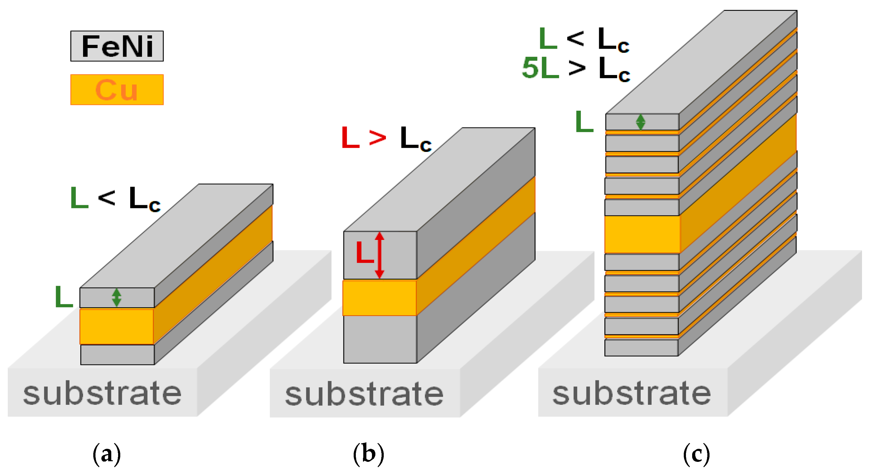
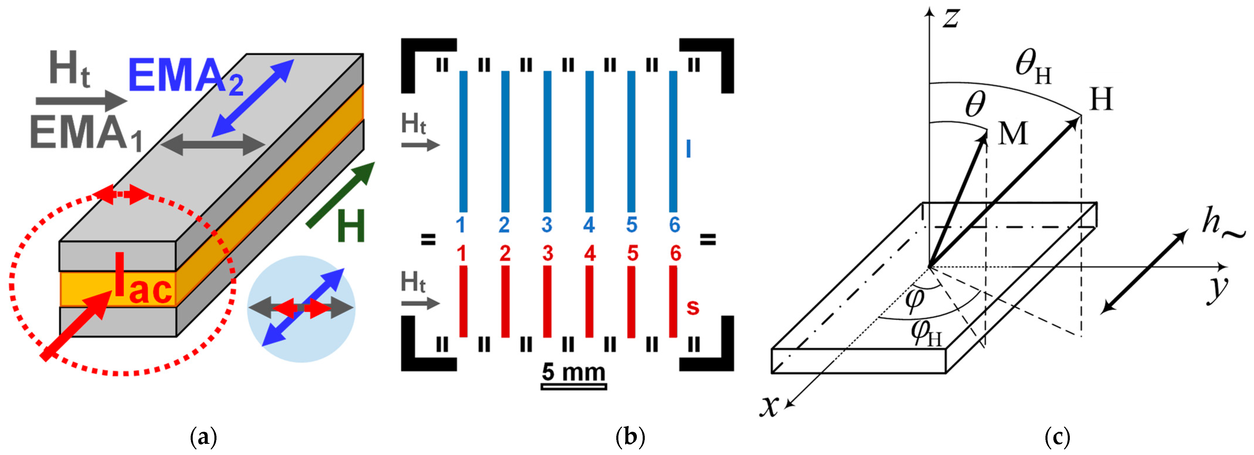
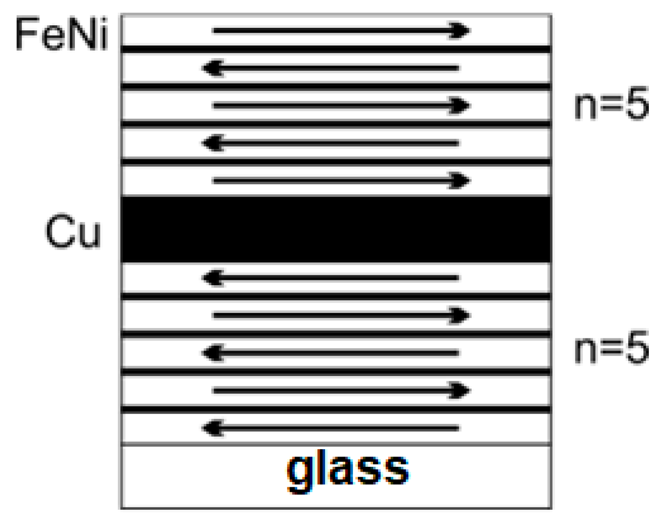
2. Experiment
3. Results and Discussion
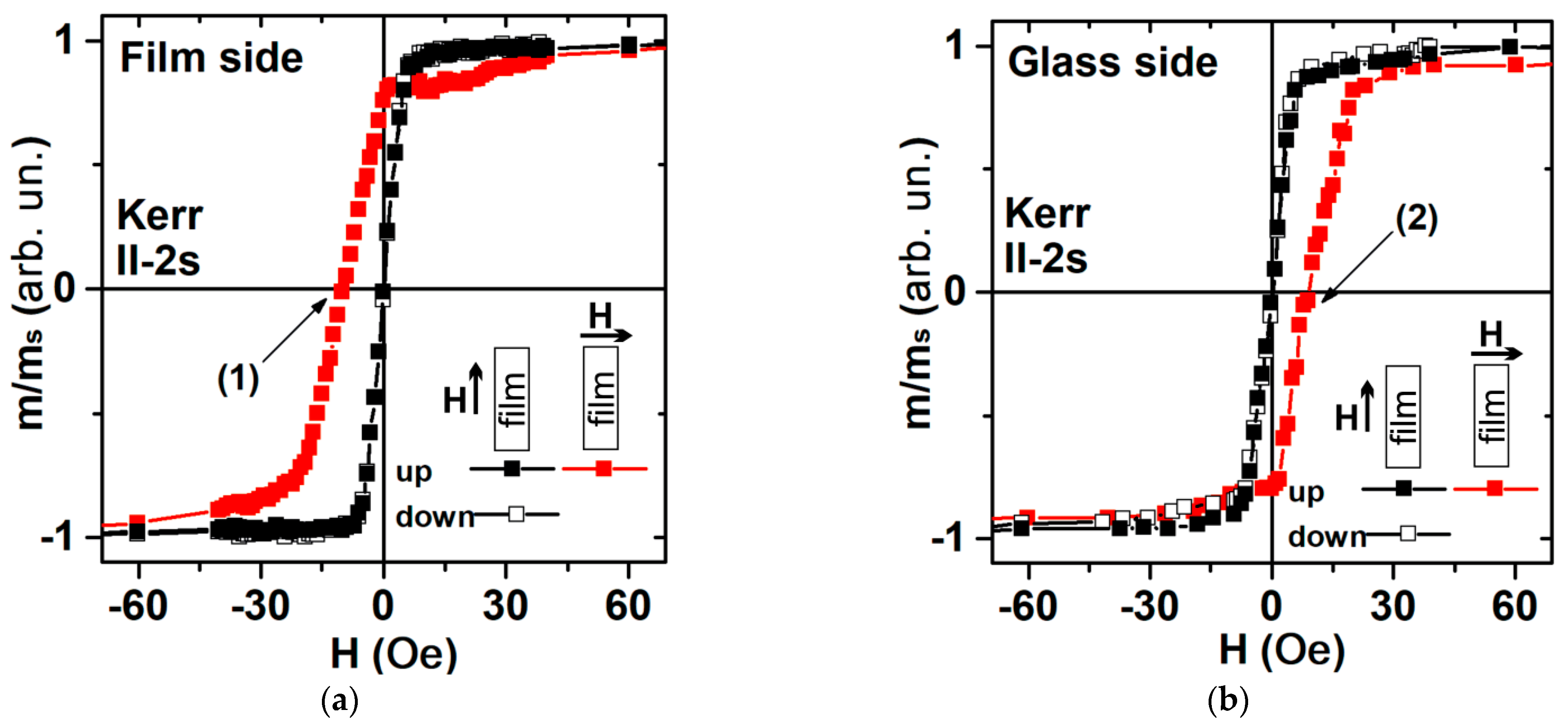
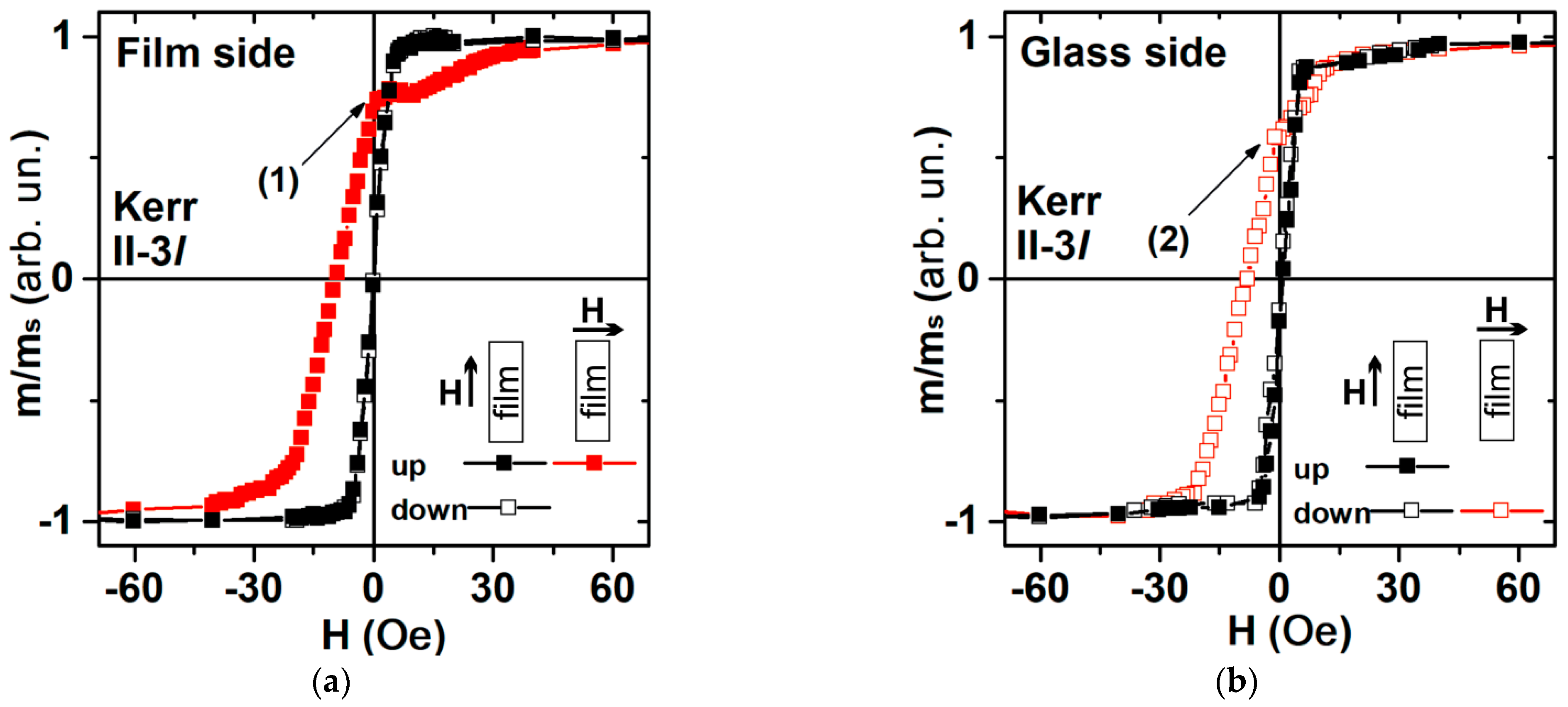
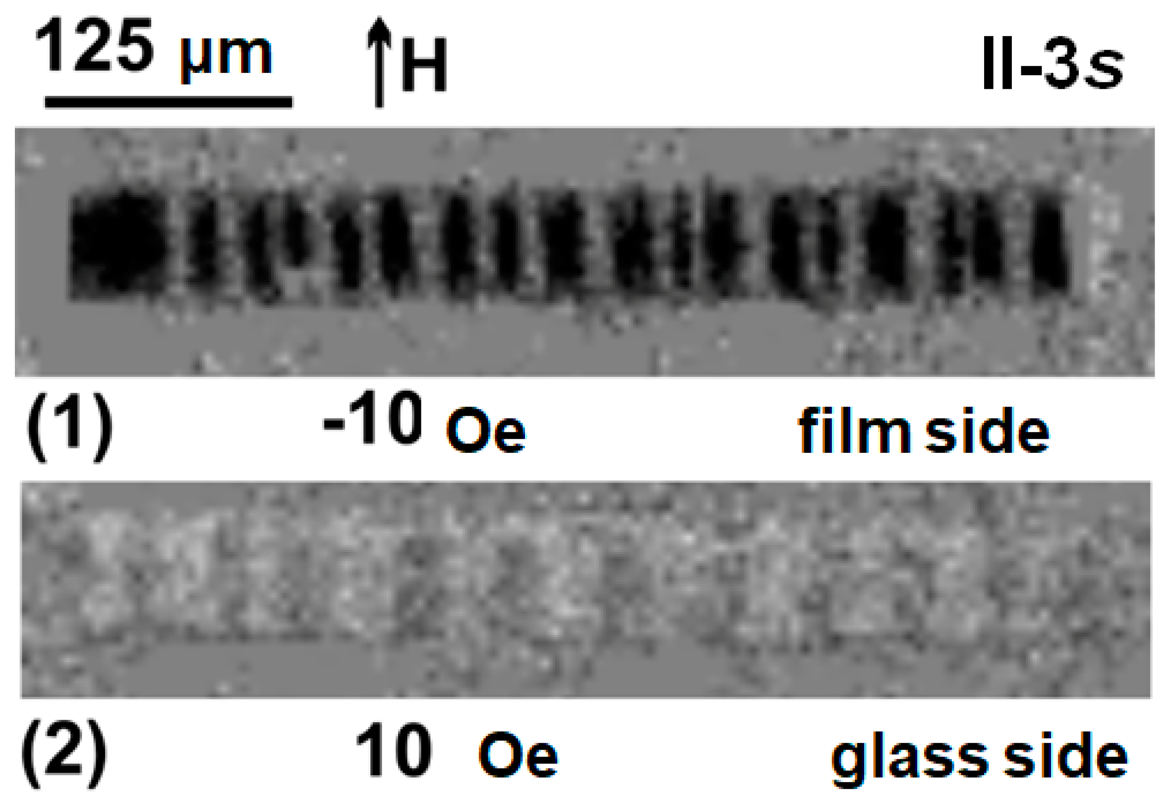
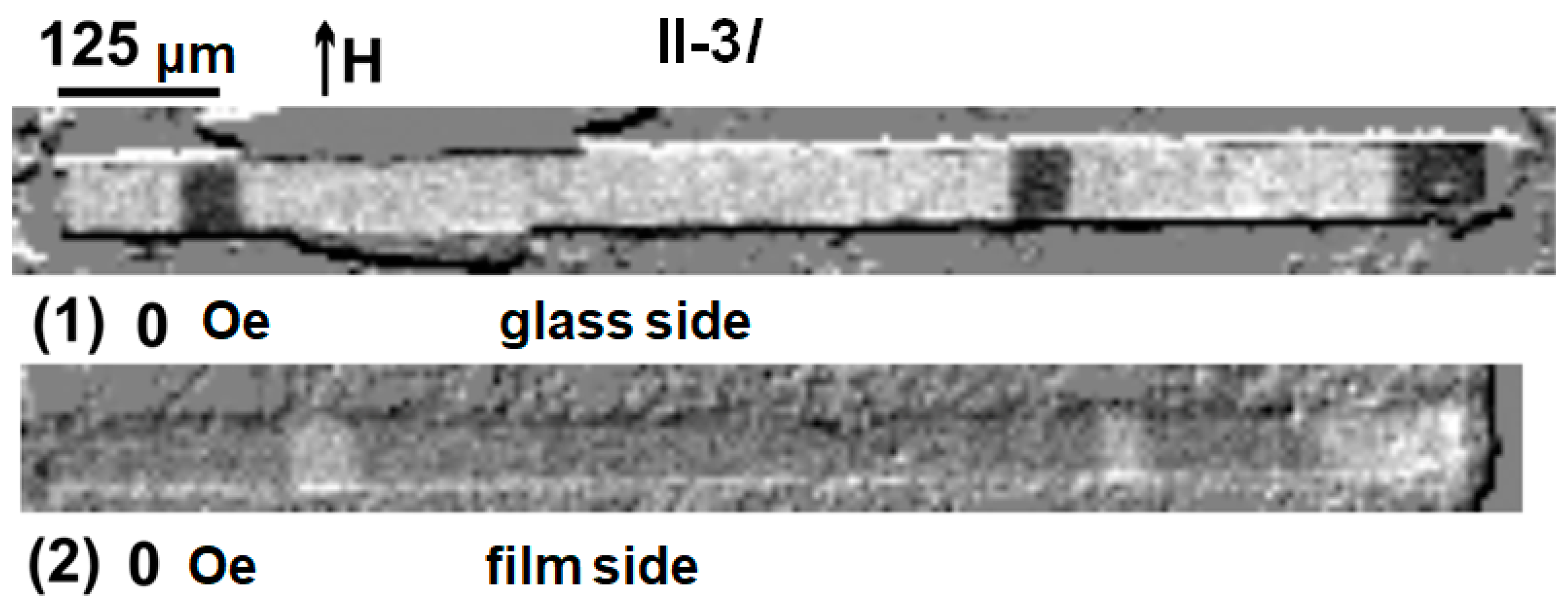
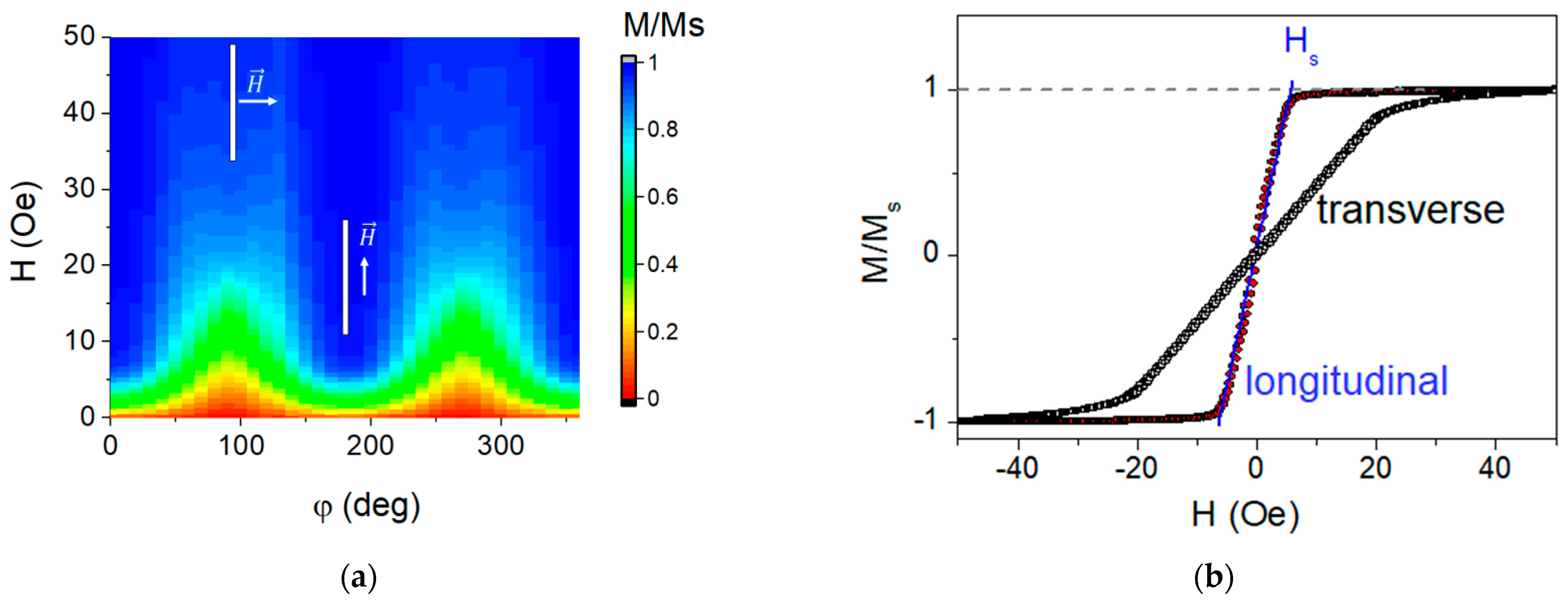
3.1. Static Magnetic Properties
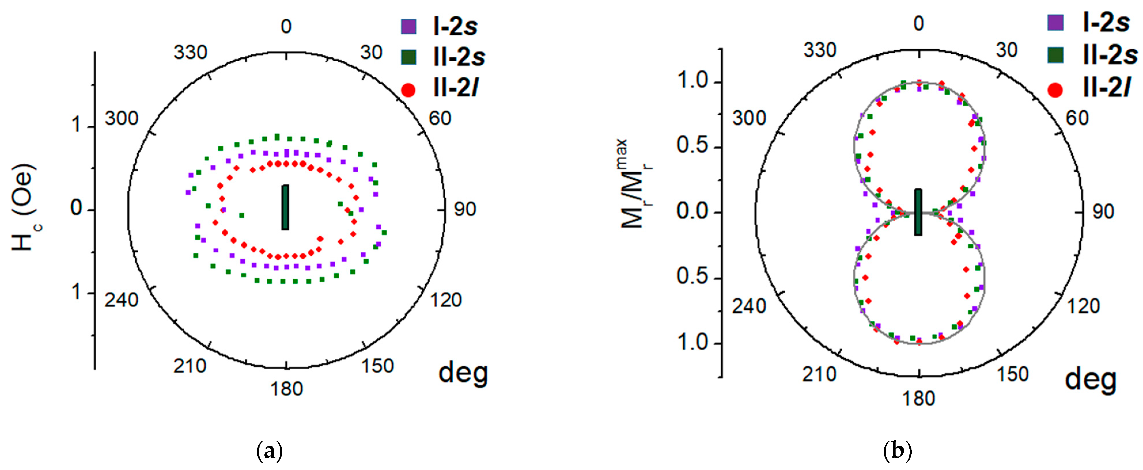
3.2. Magnetic Anisotropy of Rectangular Lithographic MI Elements
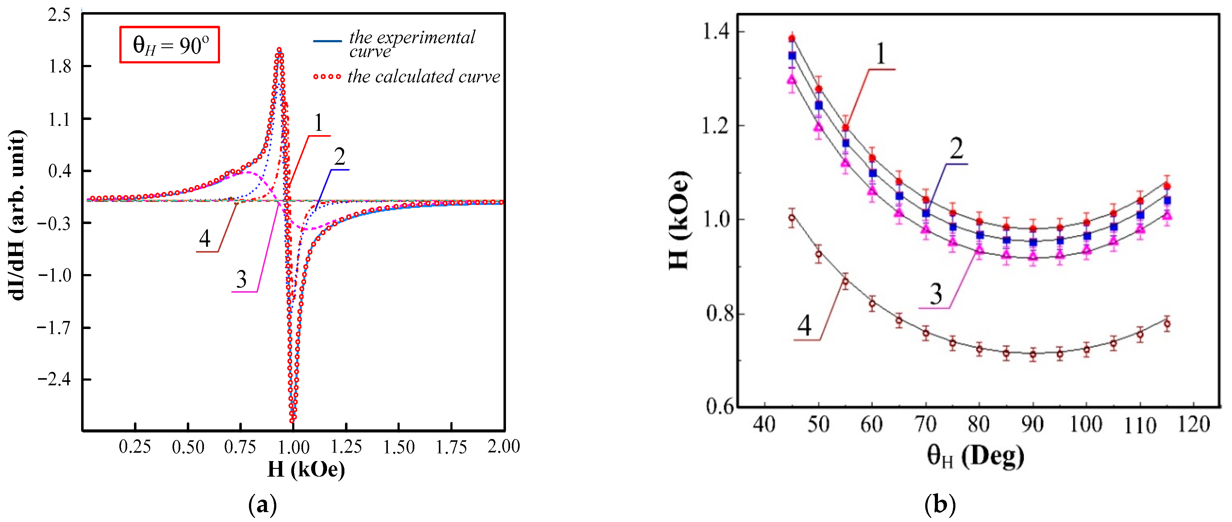
3.3. Selected Examples of Ferromagnetic and Spin-Wave Resonances
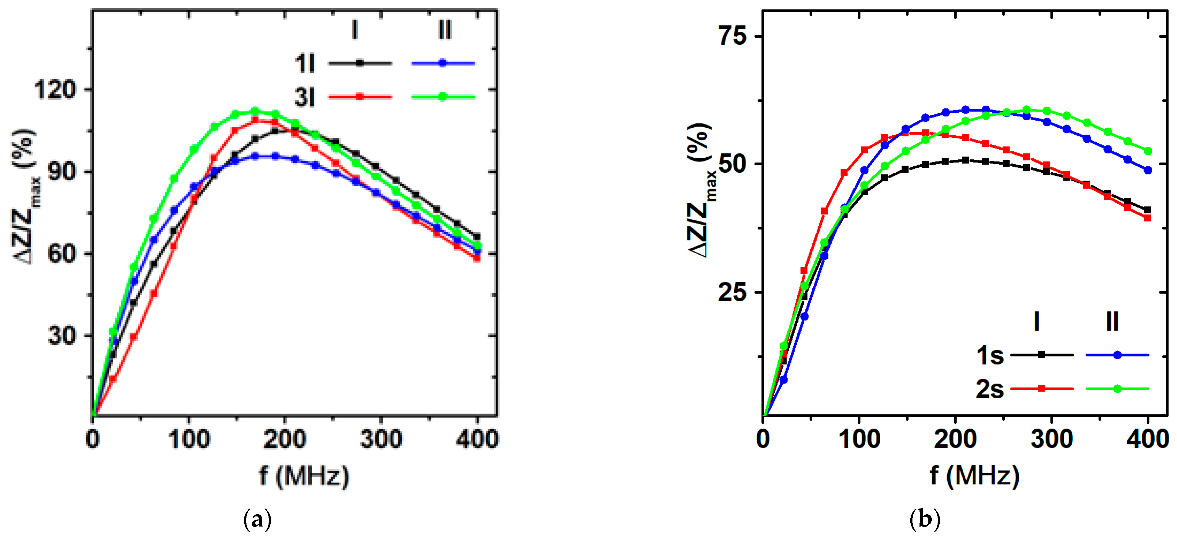
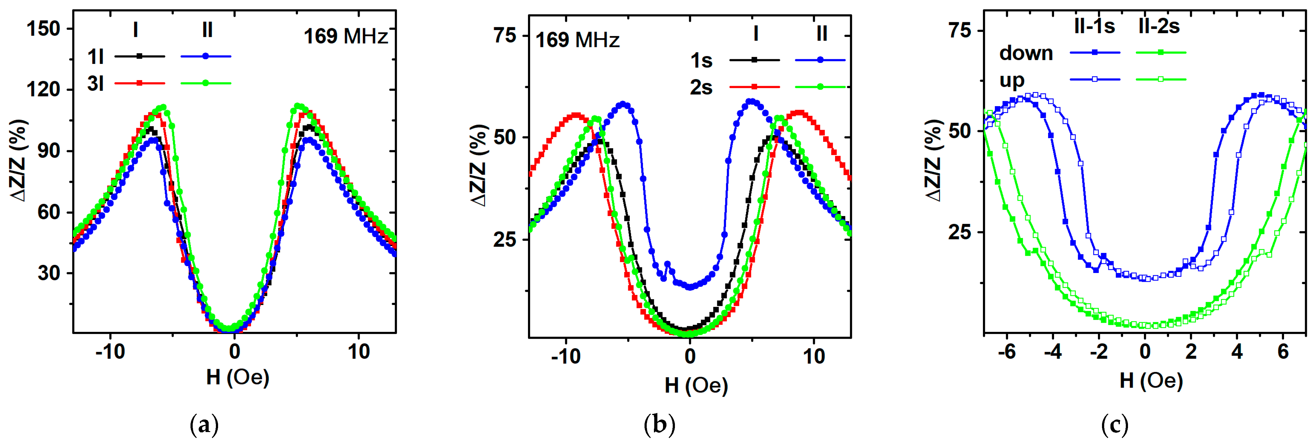
3.4. Magnetoimpedance of FeNi/Cu-Based Lithographic Rectangular Short and Long Multilayered Elements
3.5. Discussion and Future Trends
4. Conclusions
Author Contributions
Funding
Institutional Review Board Statement
Informed Consent Statement
Data Availability Statement
Acknowledgments
Conflicts of Interest
References
- Gardner, D.S.; Schrom, G.; Paillet, F.; Jamieson, B.; Karnik, T.; Borkar, S. Review of on-chip inductor structures with magnetic films. IEEE Trans. Magn. 2009, 45, 4760–4766. [Google Scholar] [CrossRef]
- Melzer, M.; Kaltenbrunner, M.; Makarov, D.; Karnaushenko, D.; Karnaushenko, D.; Sekitani, T.; Someya, T.; Schmidt, O.G. Imperceptible magnetoelectronics. Nat. Commun. 2015, 6, 6080. [Google Scholar] [CrossRef] [Green Version]
- Correa, M.A.; Bohn, F.; Viegas, A.D.C.; de Andrade, A.M.H.; Schelp, L.F.; Sommer, R.L. Magnetoimpedance effect in structure multilayered amorphous thin films. J. Phys. D Appl. Phys. 2008, 41, 175003. [Google Scholar] [CrossRef]
- Yabukami, S.; Suzuki, T.; Ajiro, N.; Kikuchi, H.; Yamaguchi, M.; Arai, K. A high frequency carrier-type magnetic field sensor using carrier suppressing circuit. IEEE Trans. Magn. 2001, 37, 2019–2021. [Google Scholar] [CrossRef]
- Kurlyandskaya, G.V.; Fernández, E.; Svalov, A.; Burgoa Beitia, A.; García-Arribas, A.; Larrañaga, A. Flexible thin-film magnetoimpedance sensors. J. Magn. Magn. Mater. 2016, 415, 91–96. [Google Scholar] [CrossRef]
- Edelstein, R.L.; Tamanaha, C.R.; Sheehan, P.E.; Miller, M.M.; Baselt, D.R.; Whitman, L.J.; Colton, R.J. The BARC biosensor applied to the detection of biological warfare agents. Biosens. Bioelectron. 2000, 14, 805–813. [Google Scholar] [CrossRef]
- Ejsing, L.; Hansen, M.F.; Menon, A. Magnetic microbead detection using the planar Hall effect. J. Magn. Magn. Mater. 2005, 293, 677–684. [Google Scholar] [CrossRef]
- Wang, T.; Chen, Y.Y.; Wang, B.C.; He, Y.; Li, H.Y.; Liu, M.; Rao, J.J.; Wu, Z.Z.; Xie, S.R.; Luo, J. A giant magnetoimpedance-based separable-type method for supersensitive detection of 10 magnetic beads at high frequency. Sens. Actuators A Phys. 2019, 300, 111656. [Google Scholar] [CrossRef]
- Buznikov, N.A.; Safronov, A.P.; Orue, I.; Golubeva, E.V.; Lepalovskij, V.N.; Svalov, A.V.; Chlenova, A.A.; Kurlyandskaya, G.V. Modelling of magnetoimpedance response of thin film sensitive element in the presence of ferrogel: Next step toward development of biosensor for in-tissue embedded magnetic nanoparticles detection. Biosens. Bioelectron. 2018, 117, 366–472. [Google Scholar] [CrossRef]
- Kraus, L. The theoretical limits of giant magneto-impedance. J. Magn. Magn. Mater. 1999, 196–197, 354–356. [Google Scholar] [CrossRef]
- Fodil, K.; Denoual, M.; Dolabdjian, C.; Harnois, M.; Senez, V. Dynamic sensing of magnetic nanoparticles in microchannel using GMI technology. IEEE Trans. Magn. 2013, 49, 93–96. [Google Scholar] [CrossRef] [Green Version]
- Uchiyama, T.; Mohri, K.; Honkura, Y.; Panina, L.V. Recent advances of pico-Tesla resolution magnetoimpedance sensor based on amorphous wire CMOS IC MI Sensor. IEEE Trans. Magn. 2012, 48, 3833–3839. [Google Scholar] [CrossRef]
- García-Arribas, A.; Fernández, E.; Svalov, A.; Kurlyandskaya, G.V.; Barandiaran, J.M. Thin-film magneto-impedance structures with very large sensitivity. J. Magn. Magn. Mater. 2016, 400, 321–326. [Google Scholar] [CrossRef]
- Kurlyandskaya, G.V.; Blyakhman, F.A.; Makarova, E.B.; Buznikov, N.A.; Safronov, A.P.; Fadeyev, F.A.; Shcherbinin, S.V.; Chlenova, A.A. Functional magnetic ferrogels: From biosensors to regenerative medicine. AIP Adv. 2020, 10, 125128. [Google Scholar] [CrossRef]
- Correa, M.A.; Viegas, A.D.C.; da Silva, R.B.; de Andrade, A.M.H.; Sommer, R.L. GMI in FeCuNbSiB\Cu multilayers. Physica B 2006, 384, 162–164. [Google Scholar] [CrossRef]
- Nakai, T. Nondestructive detection of magnetic contaminant in aluminum casting using thin film magnetic sensor. Sensors 2021, 21, 4063. [Google Scholar] [CrossRef]
- Naumova, L.I.; Milyaev, M.A.; Zavornitsyn, R.S.; Pavlova, A.Y.; Maksimova, I.K.; Krinitsina, T.P.; Chernyshova, T.A.; Proglyado, V.V.; Ustinov, V.V. High-sensitive sensing elements based on spin valves with antiferromagnetic interlayer coupling. Phys. Met. Metallogr. 2019, 120, 653–659. [Google Scholar] [CrossRef]
- Grimes, C.A. Sputter deposition of magnetic thin films onto plastic: The effect of undercoat and spacer layer composition on the magnetic properties of multilayer permalloy thin films. IEEE Trans. Magn. 1995, 31, 4109–4111. [Google Scholar] [CrossRef]
- Sugita, Y.; Fujiwara, H.; Sato, T. Critical thickness and perpendicular anisotropy of evaporated permalloy films with stripe domains. Appl. Phys. Lett. 1967, 10, 229–231. [Google Scholar] [CrossRef]
- McCord, J.; Erkartal, B.; von Hofe, T.; Kienle, L.; Quandt, E.; Roshchupkina, O.; Grenzer, J. Revisiting magnetic stripe domains—Anisotropy gradient and stripe asymmetry. J. Appl. Phys. 2013, 113, 073903. [Google Scholar] [CrossRef]
- Amos, N.; Fernández, R.; Ikkawi, R.; Lee, B.; Lavrenov, A.; Krichevsky, A.; Litvinov, D.; Khizroev, S. Magnetic force microscopy study of magnetic stripe domains in sputter deposited Permalloy thin films. J. Appl. Phys. 2008, 103, 07E732. [Google Scholar] [CrossRef]
- Svalov, A.V.; Aseguinolaza, I.R.; Garcia-Arribas, A.; Orue, I.; Barandiaran, J.M.; Alonso, J.; Fernández-Gubieda, M.L.; Kurlyandskaya, G.V. Structure and magnetic properties of thin Permalloy films near the “transcritical” state. IEEE Trans. Magn. 2010, 46, 333–336. [Google Scholar] [CrossRef]
- Kurlyandskaya, G.V.; Elbaile, L.; Alves, F.; Ahamada, B.; Barrué, R.; Svalov, A.V.; Vas’kovskiy, V.O. Domain structure and magnetization process of a giant magnetoimpedance geometry FeNi/Cu/FeNi(Cu)FeNi/Cu/FeNi sensitive element. J. Phys. Condens. Matter 2004, 16, 6561–6568. [Google Scholar] [CrossRef]
- Vas’kovskii, V.O.; Savin, P.A.; Volchkov, S.O.; Lepalovskii, V.N.; Bukreev, D.A.; Buchkevich, A.A. Nanostructuring effects in soft magnetic films and film elements with magnetic impedance. Tech. Phys. 2013, 58, 105–110. [Google Scholar] [CrossRef] [Green Version]
- Panina, L.V.; Mohri, K. Magneto-impedance in multilayer films. Sens. Actuators A 2000, 81, 71–77. [Google Scholar] [CrossRef]
- Lee, S.-Y.; Lim, Y.-S.; Choi, I.-H.; Lee, D.-I.; Kim, S.-B. Effective combination of soft magnetic materials for magnetic shielding. IEEE Trans. Magn. 2012, 48, 4550–4553. [Google Scholar] [CrossRef]
- Antonov, A.S.; Gadetskii, S.N.; Granovskii, A.B.; D’yachkov, A.L.; Paramonov, V.P.; Perov, N.S.; Prokoshin, A.F.; Usov, N.A.; Lagar’kov, A.N. Giant magnetoimpedance in amorphous and nanocrystalline multilayers. Phys. Met. Metallorgr. 1997, 83, 612–618. [Google Scholar]
- Baselt, D.R.; Lee, G.U.; Natesan, M.; Metzger, S.W.; Sheehan, P.E.; Colton, R.J. A biosensor based on magnetoresistance technology. Biosens. Bioelectron. 1998, 13, 731–739. [Google Scholar] [CrossRef]
- Naumova, L.I.; Milyaev, M.A.; Krinitsina, T.P.; Makarov, V.V.; Ryabukhina, M.V.; Chernyshova, T.A.; Maksimova, I.K.; Proglyado, V.V.; Ustinov, V.V. Microstructure and Magnetic Properties of the Gadolinium Nanolayer in a Thermo-Sensitive Spin Valve. Phys. Met. Metallogr. 2018, 119, 817–824. [Google Scholar] [CrossRef]
- Kurlyandskaya, G.V.; Chlenova, A.A.; Fernández, E.; Lodewijk, K.J. FeNi-based flat magnetoimpedance nanostructures with open magnetic flux: New topological approaches. J. Magn. Magn. Mater. 2015, 383, 220–225. [Google Scholar] [CrossRef]
- Svalov, A.V.; Gorkovenko, A.N.; Larrañaga, A.; Volochaev, M.N.; Kurlyandskaya, G.V. Structural and magnetic properties of FeNi films and FeNi-based trilayers with out-of-plane magnetization component. Sensors 2022, 22, 8357. [Google Scholar] [CrossRef] [PubMed]
- Yelon, A.; Menard, D.; Britel, M.; Ciureanu, P. Calculations of giant magnetoimpedance and of ferromagnetic resonance response are rigorously equivalent. Appl. Phys. Lett. 1996, 69, 3084–3085. [Google Scholar] [CrossRef]
- Bhagat, S.M. Metals Handbook, 9th ed.; American Society of Metals: Metals Park, OH, USA, 1986; Volume 10, p. 267. [Google Scholar]
- Komogortsev, S.V.; Vazhenina, I.G.; Kleshnina, S.A.; Iskhakov, R.S.; Lepalovskij, V.N.; Pasynkova, A.A.; Svalov, A.V. Advanced characterization of FeNi-based films for the development of magnetic field sensors with tailored functional parameters. Sensors 2022, 23, 3324. [Google Scholar] [CrossRef] [PubMed]
- Kikuchi, H.; Umezaki, T.; Shima, T.; Sumida, S.; Oe, S. Impedance change ratio and sensitivity of micromachined single-layer thin film magneto-impedance sensor. IEEE Magn. Lett. 2019, 10, 8107205. [Google Scholar] [CrossRef]
- Yabukami, S.; Kato, K.; Ohtomo, Y.; Ozawa, T.; Arai, K. A thin film magnetic field sensor of sub-pT resolution and magnetocardiogram (MCG) measurement at room temperature. J. Magn. Magn. Mater. 2009, 321, 675–678. [Google Scholar] [CrossRef]
- Fernández, E.; Lopez, A.; Garcia-Arribas, A.; Svalov, A.V.; Kurlyandskaya, G.V.; Barrainkua, A. High-frequency magnetoimpedance response of thin-film microstructures using coplanar waveguides. IEEE Trans. Magn. 2015, 51, 6100404. [Google Scholar] [CrossRef]
- Kleshnina, S.A.; Podshivalov, I.V.; Boev, N.M.; Gorchakovskii, A.A.; Solovev, P.N.; Izotov, A.I.; Burmitskikh, A.V.; Krekov, S.D.; Grushevskii, E.O.; Negodeeva, I.A. Ferrometer for Thin Magnetic Films; Patent № RU 2795378C1; 3 May 2023. Available online: https://www.fips.ru/cdfi/fips.dll/en?ty=29&docid=2795378 (accessed on 1 May 2023).
- García-Arribas, A.; Fernández, E.; Barrainkua, A.; Svalov, A.V.; Kurlyandskaya, G.V.; Barandiaran, J.M. Comparison of Micro-Fabrication Routes for Magneto-Impedance Elements: Lift-Off and Wet-Etching. IEEE Trans. Magn. 2012, 48, 1601–1604. [Google Scholar] [CrossRef]
- Belyaev, B.A.; Boev, N.M.; Izotov, A.V.; Solovev, P.N. Domain structure and magnetization re-versal in multilayer structures consisting of thin permalloy films separated with nonmagnetic inter-layers. Russ. Phys. J. 2021, 64, 1160–1167. [Google Scholar] [CrossRef]
- Schäfer, R. Magnetooptical domain studies in coupled magnetic multilayers. J. Magn. Magn. Mater. 1995, 148, 226–231. [Google Scholar] [CrossRef]
- Wei, X.-H.; Skomski, R.; Sun, Z.-G.; Sellmyer, D.J. Proteresis in Co: CoO core-shell nanoclusters. J. Appl. Phys. 2008, 103, 07D514. [Google Scholar] [CrossRef] [Green Version]
- Netzelmann, U. Ferromagnetic resonance of particulate magnetic recording tapes. J. Appl. Phys. 1990, 68, 1800–1807. [Google Scholar] [CrossRef]
- Schmool, D.S.; Rocha, R.; Sousa, J.B.; Santos, J.A.M.; Kakazei, G.N.; Garitaonandia, J.S.; Lezama, L. The role of dipolar interactions in magnetic nanoparticles: Ferromagnetic resonance in discontinuous magnetic multilayers. J. Appl. Phys. 2007, 101, 103907. [Google Scholar] [CrossRef]
- Dubowik, J. Shape anisotropy of magnetic heterostructures. Phys. Rev. B 1996, 54, 1088–1091. [Google Scholar] [CrossRef] [PubMed]
- Aharoni, A. Demagnetizing factors for rectangular ferromagnetic prisms. J. Appl. Phys. 1998, 83, 3432–3434. [Google Scholar] [CrossRef]
- Meshcheryakov, V.F. Resonance modes of layered ferromagnets in a transverse magnetic field. J. Exp. Theor. Phys. Lett. 2002, 76, 707–710. [Google Scholar] [CrossRef]
- Suhl, H. Ferromagnetic Resonance in Nickel Ferrite Between One and Two Kilomegacycles. Phys. Rev. 1955, 97, 555–557. [Google Scholar] [CrossRef]
- Smit, J.; Beljers, H.G. Ferromagnetic resonance absorption in BaFe12O12, a highly anisotropic crystal. Philips Res. Rep. 1955, 10, 113–130. [Google Scholar]
- Artman, J.O. Ferromagnetic Resonance in Metal Single Crystals. Phys. Rev. 1957, 105, 74–84. [Google Scholar] [CrossRef]
- Kittel, C. Excitation of spin waves in a ferromagnet by a uniform rf field. Phys. Rev. 1958, 110, 1295–1297. [Google Scholar] [CrossRef]
- Vazhenina, I.G.; Iskhakov, R.S.; Yakovchuk, V.Y. Features of the angular dependences of the parameters of the ferromagnetic and spin-wave resonance spectra of magnetic films. Phys. Met. Metallogr. 2022, 123, 1084–1090. [Google Scholar] [CrossRef]
- Vazhenina, I.G.; Iskhakov, R.S.; Milyaev, M.A.; Naumova, L.I.; Rautsky, M.V. Spin Wave Resonance in the [(Co0.88Fe0.12)/Cu]N Synthetic Antiferromagnet. Tech. Phys. Lett. 2020, 46, 1076–1079. [Google Scholar] [CrossRef]
- Ignatchenko, V.A.; Iskhakov, R.S. Spin Waves in Stochastic Anisotropic Materials. Sov. Phys.-JETP 1977, 45, 526. [Google Scholar]
- Hoekstra, B.; van Stapele, R.P.; Robertson, J.M. Spin-wave resonance spectra of inhomogeneous bubble garnet films. J. Appl. Phys. 1977, 48, 382–395. [Google Scholar] [CrossRef]
- Iskhakov, R.S.; Stolyar, S.V.; Chekanova, L.A.; Vazhenina, I.G. Spin-Wave Resonance in One-Dimensional Magnonic Crystals by an Example of Multilayer Co–P Films. Phys. Solid State 2020, 62, 1861–1867. [Google Scholar] [CrossRef]
- Iskhakov, R.S.; Moroz, Z.M.; Chekanova, L.A.; Shalygina, E.E.; Shepeta, N.A. Ferromagnetic and spin-wave resonance in Co/Pd/CoNi multilayer films. Phys. Solid State 2003, 45, 890–894. [Google Scholar]
- van Stapele, R.P.; Greidanus, F.J.A.M.; Smits, J.W. The spin-wave spectrum of layered magnetic thin films. J. Appl. Phys. 1985, 57, 1282–1290. [Google Scholar] [CrossRef]
- Knobel, M.; Vazquez, M.; Kraus, L. Giant Magnetoimpedance in Handbook of Magnetic Materials; Buschow, K.H.J., Ed.; Elsevier: Amsterdam, The Netherlands, 2003; pp. 497–564. [Google Scholar]
- Rebello, A.; Mahendirana, R. Influence of length and measurement geometry on magnetoimpedance in La0.7Sr0.3MnO3. Appl. Phys. Lett. 2010, 96, 032502. [Google Scholar] [CrossRef] [Green Version]
- Dolabdjian, C.; Ménard, D. Giant magneto-impedance (GMI) magnetometers. In High Sensitivity Magnetometers; Grosz, A., Haji-Sheikh, M.J., Mukhopadhyay, S.C., Eds.; Springer: Berlin/Heidelberg, Germany, 2017; pp. 103–126. [Google Scholar]
- Buznikov, N.A.; Svalov, A.V.; Kurlyandskaya, G.V. Influence of the parameters of permalloy-based multilayer film structures on the sensitivity of magnetic impedance effect. Phys. Met. Metallogr. 2021, 122, 223–229. [Google Scholar] [CrossRef]
- Bukreev, D.A.; Derevyanko, M.S.; Moiseev, A.A.; Semirov, A.V. Effect of tensile stress on cobalt-based amorphous wires impedance near the magnetostriction compensation temperature. J. Magn. Magn. Mater. 2020, 500, 166436. [Google Scholar] [CrossRef]
- Nowicki, M.; Gazda, P.; Szewczyk, R.; Marusenkov, A.; Nosenko, A.; Kyrylchuk, V. Strain dependence of hysteretic giant magnetoimpedance effect in Co-based amorphous ribbon. Materials 2019, 12, 2110. [Google Scholar] [CrossRef] [Green Version]
- Nakai, T.; Ishiyama, K.; Yamasaki, J. Study of hysteresis for steplike giant magnetoimpedance sensor based on magnetic energy. J. Magn. Magn. Mater. 2008, 320, e958–e962. [Google Scholar] [CrossRef]
- Antonov, A.; Gadetsky, S.; Granovsky, A.; D’yatckov, A.; Sedova, M.; Perov, N.; Usov, N.; Furmanova, T.; Lagar’kov, A. High-frequency giant magneto-impedance in multilayered magnetic films. Phys. A Stat. Mech. Its Appl. 1997, 241, 414–419. [Google Scholar] [CrossRef]
- Yang, Z.; Liu, Y.; Lei, C.; Sun, X.C.; Zhou, Y. Ultrasensitive detection and quantification of E. coli O157:H7 using a giant magnetoimpedance sensor in an open-surface microfluidic cavity covered with an antibody-modified gold surface. Microchim. Acta 2016, 183, 1831–1837. [Google Scholar] [CrossRef]
- Kurlyandskaya, G.V.; Levit, V.I. Advanced materials for drug delivery and biosensors based on magnetic label detection. Mater. Sci. Eng. C 2007, 27, 495–503. [Google Scholar] [CrossRef]
- Fodil, K.; Denoual, M.; Dolabdijan, C.; Treizebre, A.; Senez, V. In-flow detection of ultra-small magnetic particles by an integrated giant magnetic impedance sensor. Appl. Phys. Lett. 2016, 108, 173701. [Google Scholar] [CrossRef]
- Devkota, J.; Wang, C.; Ruiz, A.P.; Mohapatra, S.; Mukherjee, P.; Srikanth, H.; Phan, M.H. Detection of low-concentration superparamagnetic nanoparticles using an integrated radio frequency magnetic biosensor. J. Appl. Phys. 2013, 113, 104701. [Google Scholar] [CrossRef]
- Sukstanskii, A.; Korenivski, V.; Gromov, A. Impedance of a ferromagnetic sandwich strip. J. Appl. Phys. 2001, 89, 775–782. [Google Scholar] [CrossRef]
- Zotov, N.; Ludwig, A. Atomic mechanisms of interdiffusion in metallic multilayers. Mater. Sci. Eng. C 2007, 27, 1470–1474. [Google Scholar] [CrossRef]


| Sample | ||||
|---|---|---|---|---|
| , Oe | , Oe | , Oe | , Oe | |
| 35.1 ± 0.1 | 25 ± 1 | 1.7 ± 0.1 | 5.5 ± 0.1 | |
| 34.9 ± 0.1 | 25 ± 1 | 3.4 ± 0.1 | 6.0 ± 0.1 | |
| , G | The Perpendicular Anisotropy Field of the Individual Mode Ha, Oe | |||
|---|---|---|---|---|
| 1 | 2 | 3 | 4 | |
| 820 | 120 ÷ 420 | 200 ÷ 1000 | (750 ÷ 1240) | 4500 ÷ 5000 |
| Area | , Oe | ||
|---|---|---|---|
| A | 5.0 ± 0.5 | 0.017 ± 0.002 | 0.014 ± 0.002 |
| B | 1.5 ± 0.1 | 0.035 ± 0.004 | 0.042 ± 0.004 |
| C | 9.0 ± 0.9 | - | - |
Disclaimer/Publisher’s Note: The statements, opinions and data contained in all publications are solely those of the individual author(s) and contributor(s) and not of MDPI and/or the editor(s). MDPI and/or the editor(s) disclaim responsibility for any injury to people or property resulting from any ideas, methods, instructions or products referred to in the content. |
© 2023 by the authors. Licensee MDPI, Basel, Switzerland. This article is an open access article distributed under the terms and conditions of the Creative Commons Attribution (CC BY) license (https://creativecommons.org/licenses/by/4.0/).
Share and Cite
Melnikov, G.Y.; Vazhenina, I.G.; Iskhakov, R.S.; Boev, N.M.; Komogortsev, S.V.; Svalov, A.V.; Kurlyandskaya, G.V. Magnetic Properties of FeNi/Cu-Based Lithographic Rectangular Multilayered Elements for Magnetoimpedance Applications. Sensors 2023, 23, 6165. https://doi.org/10.3390/s23136165
Melnikov GY, Vazhenina IG, Iskhakov RS, Boev NM, Komogortsev SV, Svalov AV, Kurlyandskaya GV. Magnetic Properties of FeNi/Cu-Based Lithographic Rectangular Multilayered Elements for Magnetoimpedance Applications. Sensors. 2023; 23(13):6165. https://doi.org/10.3390/s23136165
Chicago/Turabian StyleMelnikov, Grigory Yu., Irina G. Vazhenina, Rauf S. Iskhakov, Nikita M. Boev, Sergey V. Komogortsev, Andrey V. Svalov, and Galina V. Kurlyandskaya. 2023. "Magnetic Properties of FeNi/Cu-Based Lithographic Rectangular Multilayered Elements for Magnetoimpedance Applications" Sensors 23, no. 13: 6165. https://doi.org/10.3390/s23136165