
Compact Wideband Groove Gap Waveguide Bandpass Filters Manufactured with 3D Printing and CNC Milling Techniques
 , and
, and 
Abstract
:1. Introduction
2. Design of the Wideband GGW Bandpass Filter
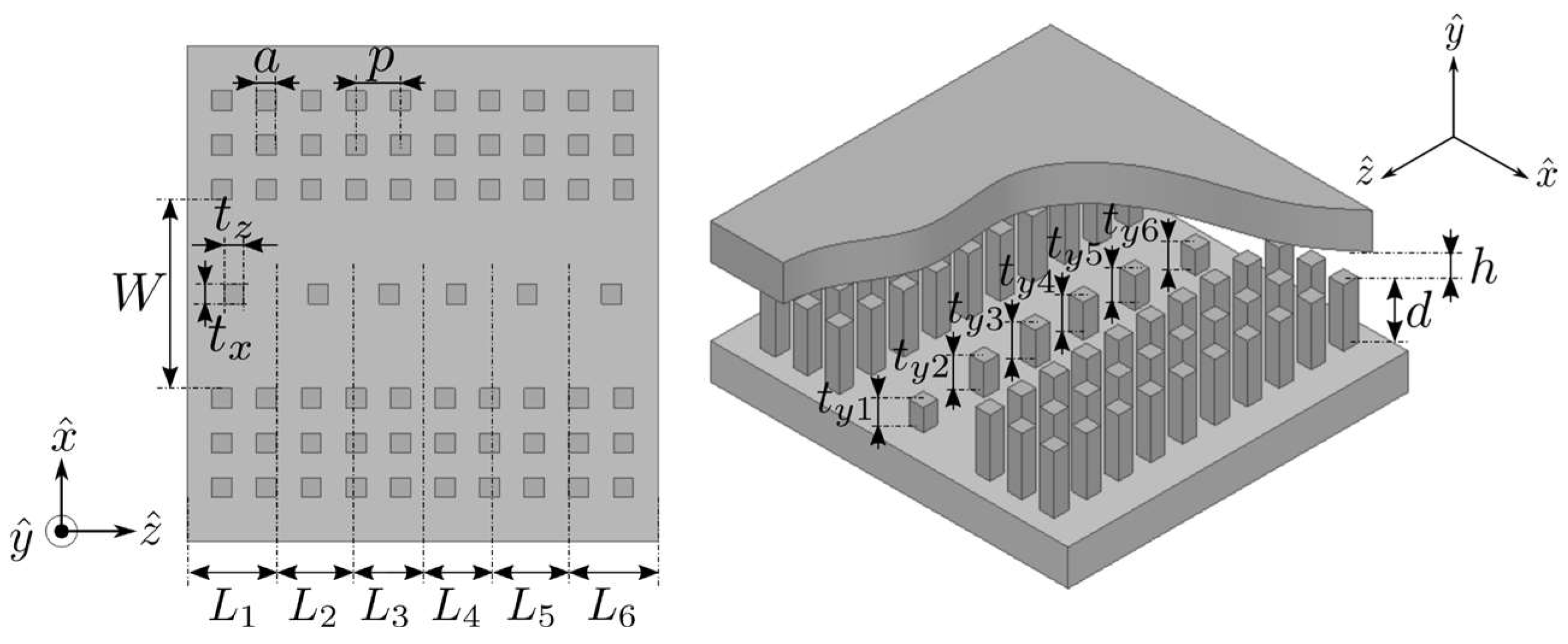
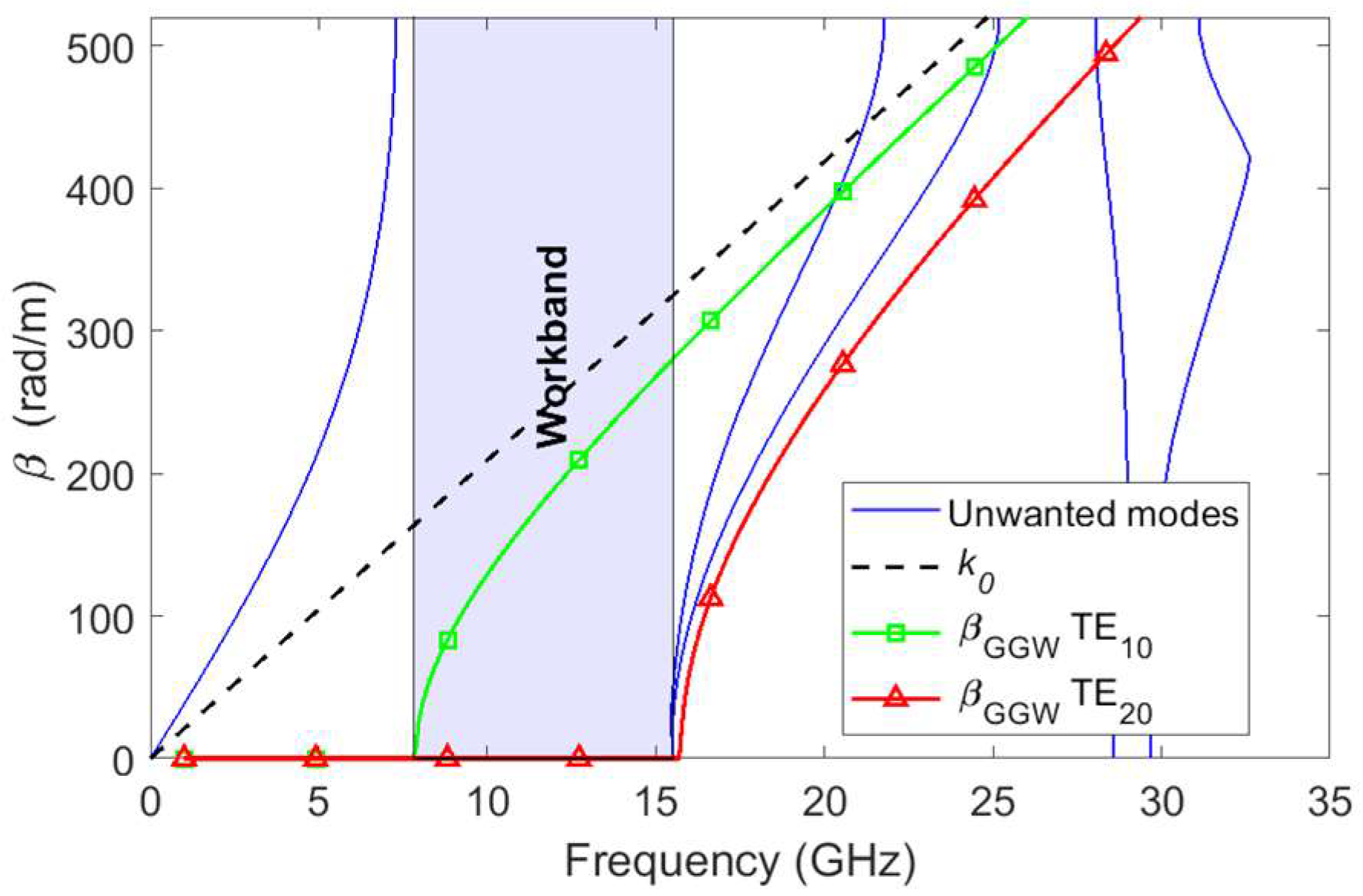
2.1. GGW Design
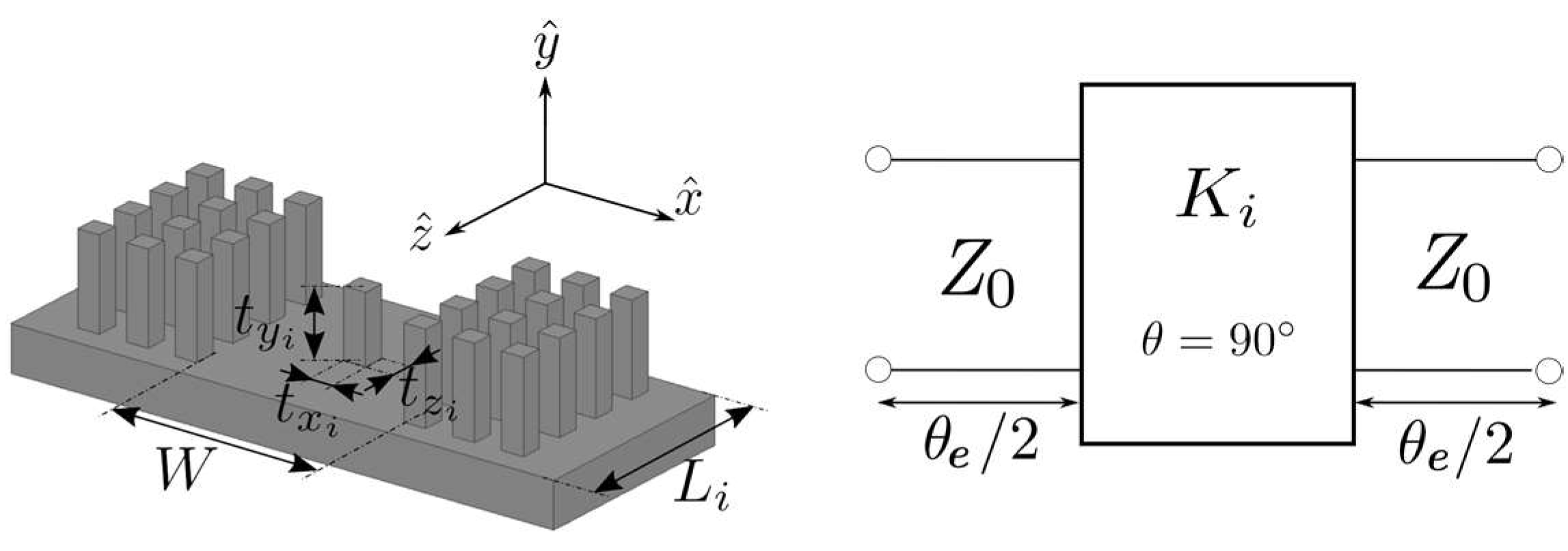
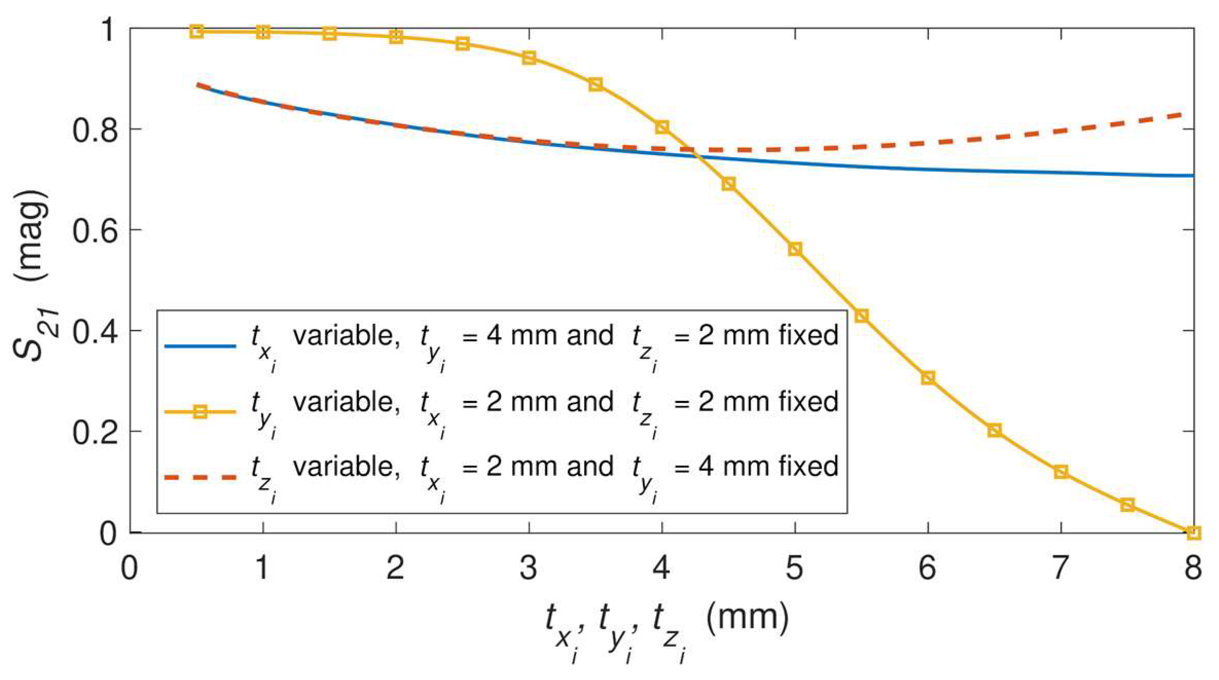
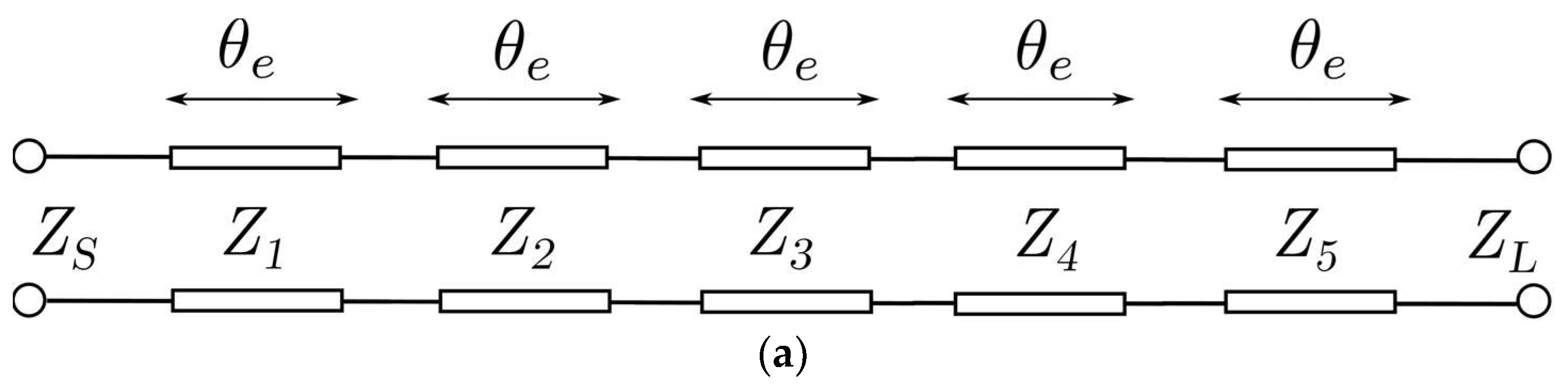
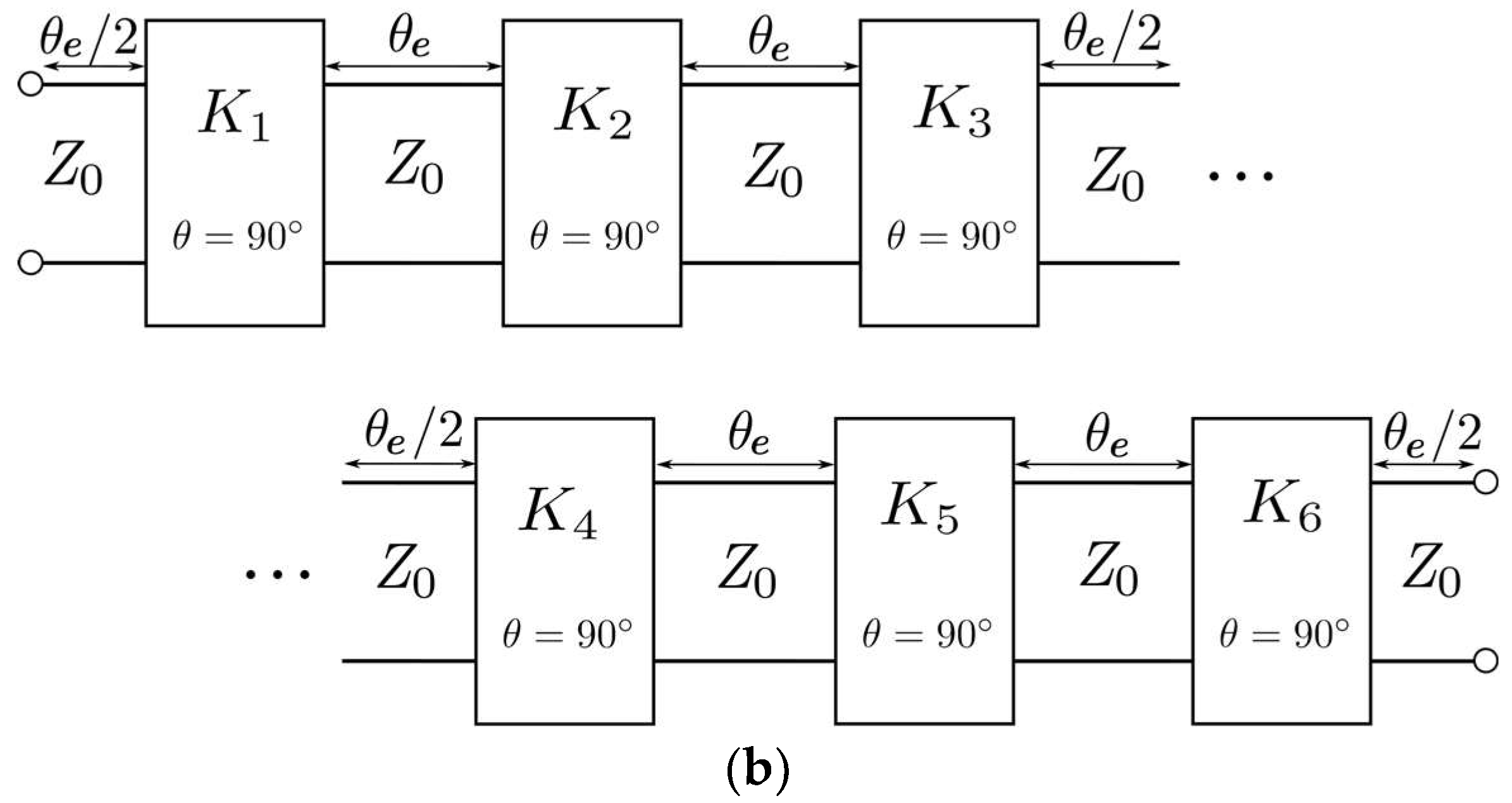
2.2. Stepped Impedance Analysis
2.3. Filter Design
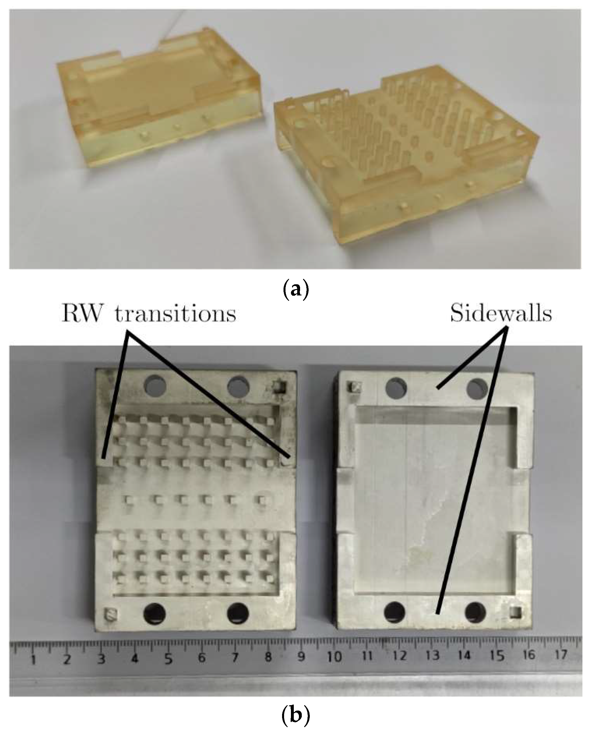
3. Fabrication
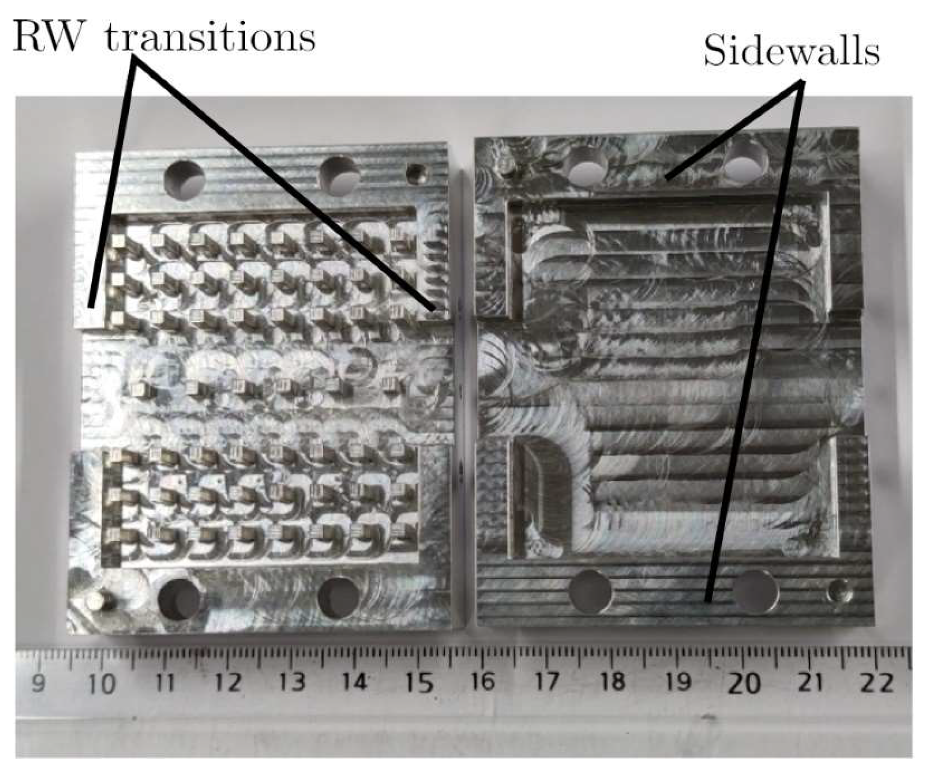
3.1. CNC Machining Technique
3.2. 3D Printing Technique
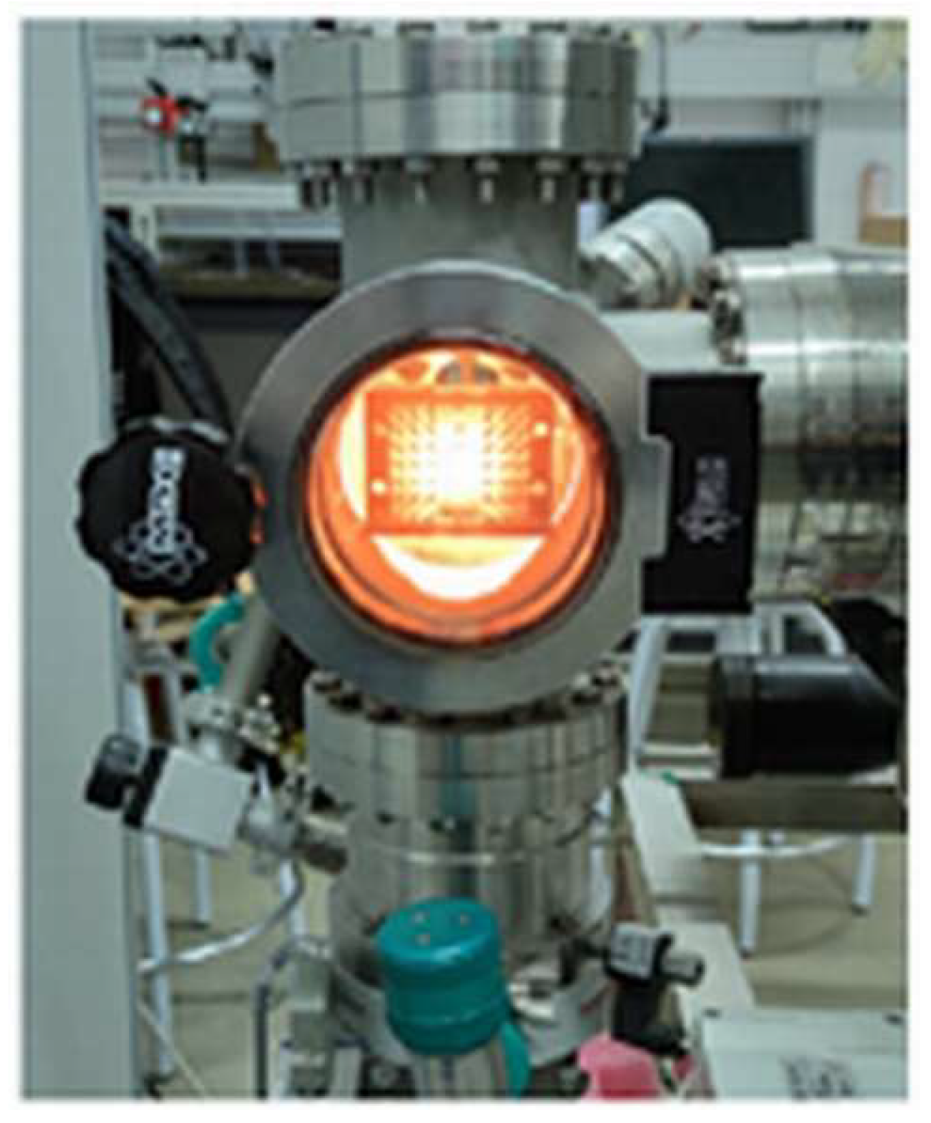
3.2.1. High-Vacuum Evaporation Technique
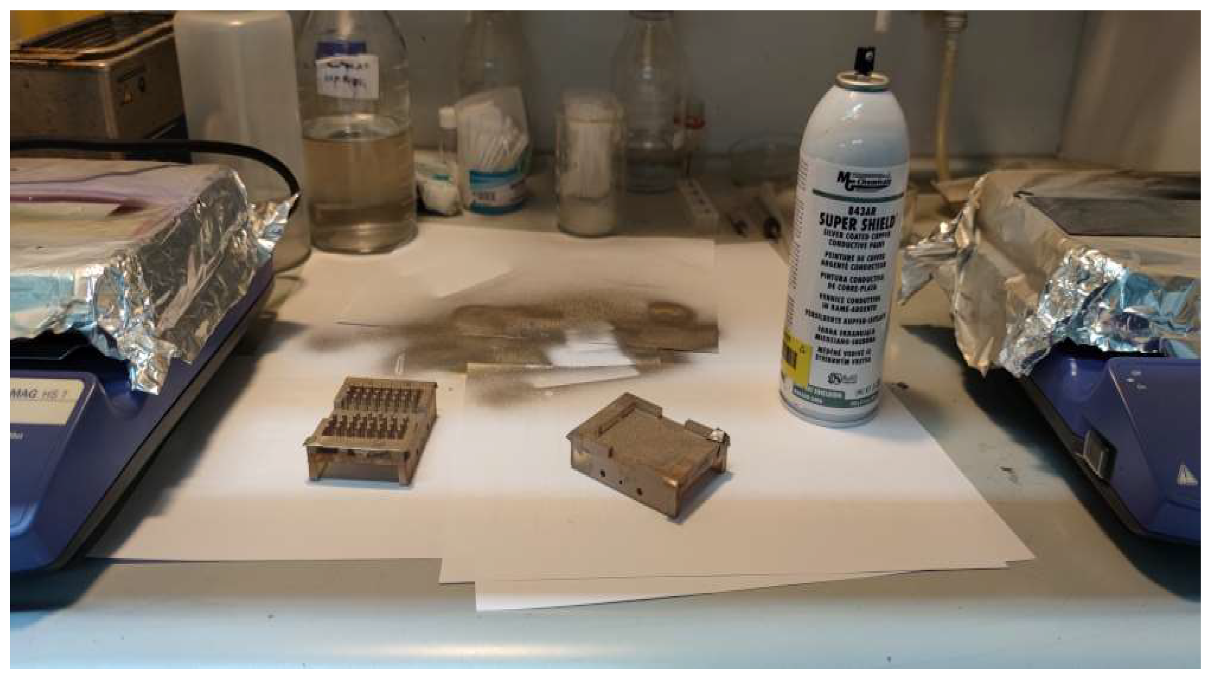
3.2.2. Conductive Paint Spray System
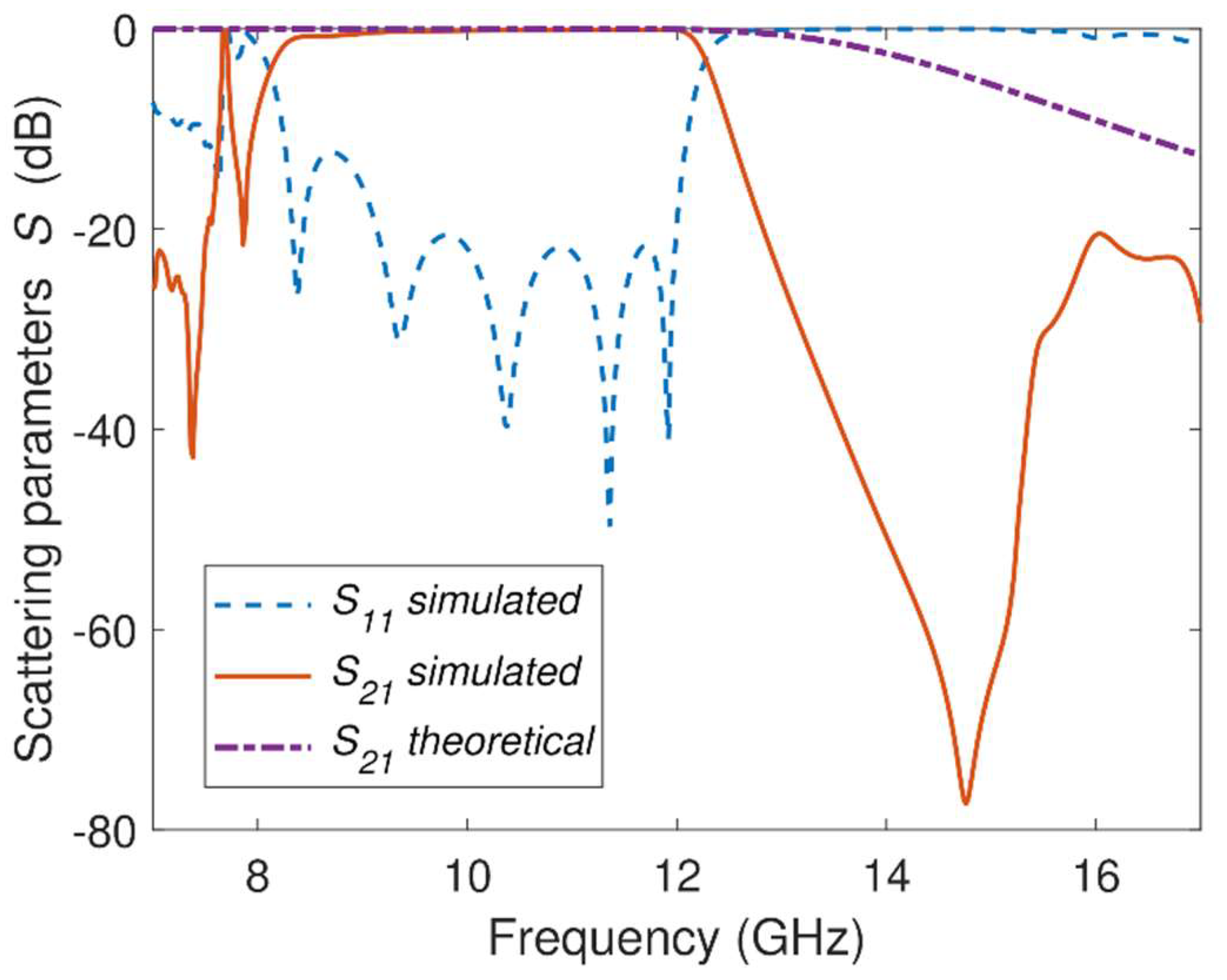
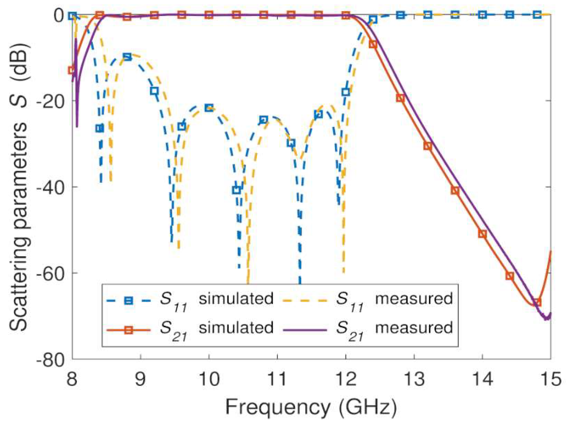
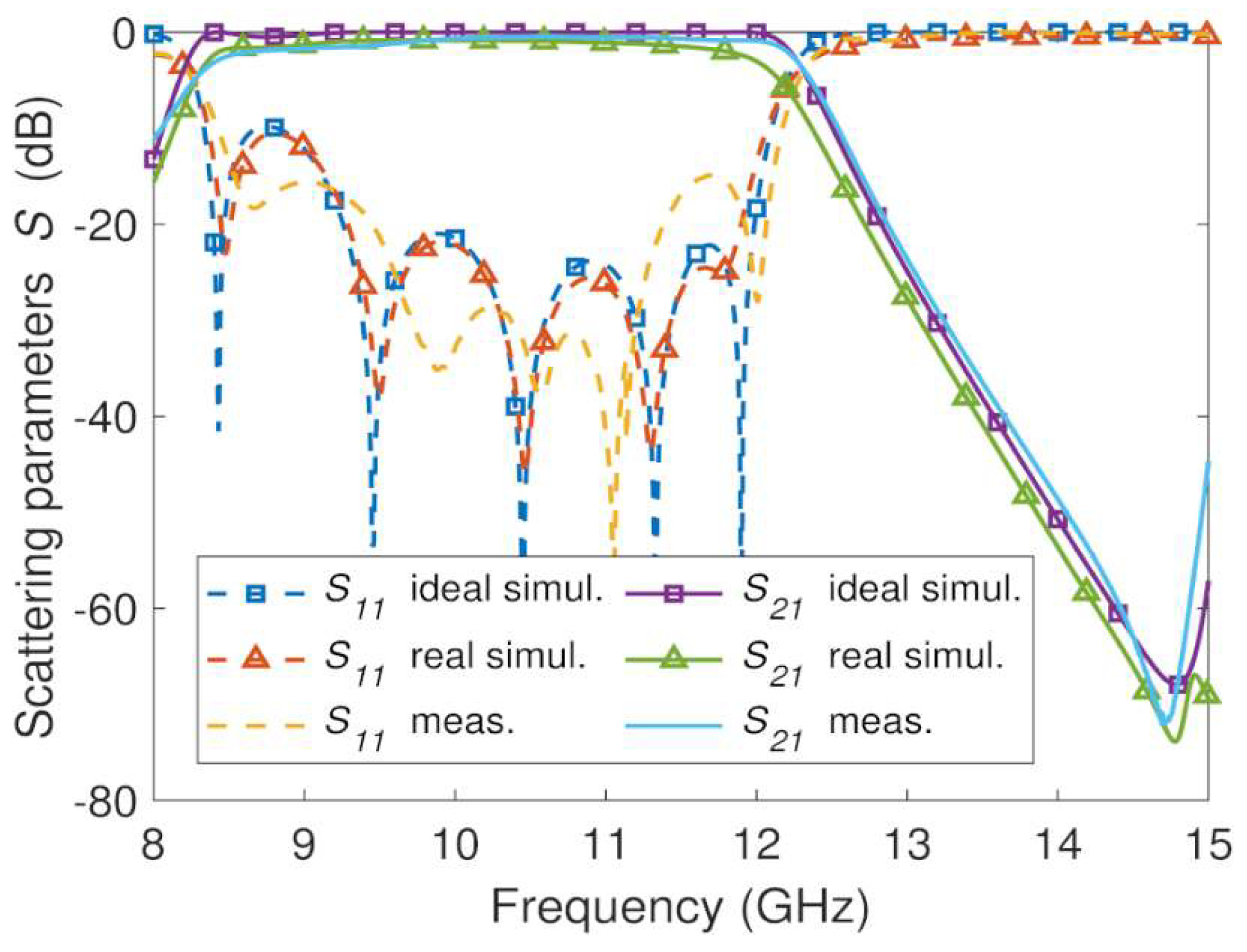
4. Experimental Results
5. Conclusions
Author Contributions
Funding
Institutional Review Board Statement
Informed Consent Statement
Data Availability Statement
Conflicts of Interest
References
- Boria, V.E.; Gimeno, B. Waveguide filters for satellites. IEEE Microw. Mag. 2007, 8, 60–70. [Google Scholar] [CrossRef]
- Hong, J.S.; Lancaster, M. Microstrip Filters for RF/Microwave Applications; Wiley: New York, NY, USA, 2001. [Google Scholar]
- Máximo-Gutiérrez, C.; Hinojosa, J.; Martínez-Viviente, F.L.; Alvarez-Melcon, A. Design of high-performance microstrip and coplanar low-pass filter based on electromagnetic bandgap (EBG) structures. AEU-Int. J. Electron. Commun. 2020, 123, 153311. [Google Scholar] [CrossRef]
- Magnuski, M.; Noga, A.; Wójcik, D. Modified triple-tuned bandpass filter with two concurrently tuned transmission zeros. Sensors 2022, 22, 9760. [Google Scholar] [CrossRef]
- Hinojosa, J.; Saura-Rodenas, A.; Avarez-Melcon, A.; Martínez-Viciente, F.L. Reconfigurables coplanar waveguide (CPW) and half-mode substrate integrated wawvguide (HMSIW) band-stop filters using varactor-loaded metamaterials-inspired open resonator. Materials 2018, 11, 39. [Google Scholar] [CrossRef] [Green Version]
- Máximo-Gutiérrez, C.; Hinojosa, J.; Alvarez-Melcon, A. Design of wide band-pass substrate integrated waveguide (SIW) filters based on stepped impedances. AEU-Int. J. Electron. Commun. 2019, 100, 1–8. [Google Scholar] [CrossRef]
- Iqbal, A.; Tiang, J.J.; Wong, S.K.; Alibakhshikenari, M.; Falcone, F.; Limitri, E. Multimode HMSIW-based bandpass filter with improved selectivity for fifth-generation (5G) RF front-ends. Sensors 2020, 20, 7320. [Google Scholar] [CrossRef] [PubMed]
- Belenguer, A.; Esteban, H.; Boria, V.E. Novel empty substrate integrated waveguide for high-performance microwave integrated circuits. IEEE Trans. Microw. Theory Techn. 2014, 62, 832–839. [Google Scholar] [CrossRef] [Green Version]
- Bigelli, F.; Mencarelli, D.; Farina, M.; Venanzoni, G.; Scalmati, P.; Renghini, C.; Morini, A. Design and fabrication of a dielectricless substrate-integrated waveguide. IEEE Trans. Compon. Packag. Manuf. Technol. 2016, 6, 256–261. [Google Scholar] [CrossRef]
- Parment, F.; Ghiotto, A.; Vuong, T.P.; Duchamp, J.M.; Wu, K. Air-filled substrate integrated waveguide for low-loss and high power-handling millimeter-wave substrate integrated circuits. IEEE Trans. Microw. Theory Techn. 2015, 63, 1228–1238. [Google Scholar] [CrossRef]
- Jin, L.; Lee, R.M.A.; Robertson, I. Analysis and design of a novel low-loss hollow substrate integrated waveguide. IEEE Trans. Microw. Theory Techn. 2014, 62, 1616–1624. [Google Scholar] [CrossRef] [Green Version]
- Ranjkesh, N.; Shahabadi, M. Reduction of dielectric losses in substrate integrated waveguide. Electron. Lett. 2006, 42, 1230–1231. [Google Scholar] [CrossRef]
- Belenguer, A.; Esteban, H.; Borja, A.L.; Boria, V.E. Empty SIW technologies: A major step toward realizing low-cost and low-loss microwave circuits. IEEE Microw. Mag. 2019, 20, 24–45. [Google Scholar] [CrossRef] [Green Version]
- Belenguer, A.; Fernandez, M.D.; Ballesteros, J.A.; Esteban, H.; Boria, V.E. Experimental study in Ku-band of the propagation inside empty substrate integrated waveguides. In Proceedings of the 2016 European Microwave Conference, London, UK, 4–6 October 2016; pp. 639–642. [Google Scholar]
- Ballesteros, J.A.; Diaz-Caballero, E.; Fernandez, M.D.; Esteban, H.; Belenguer, A.; Boria, V.E. Performance comparison of a four-pole folded filter realized with standard and empty substrate integrated waveguide technologies. In Proceedings of the 2017 European Microwave Conference, Nuremberg, Germany, 10–12 October 2017; pp. 412–415. [Google Scholar]
- Belenguer, A.; Fernandez, M.D.; Ballesteros, J.A.; De Dios, J.J.; Esteban, H.; Boria, V.E. Compact multilayer filter in empty substrate integrated waveguide with transmission zeros. IEEE Trans. Microw. Theory Techn. 2018, 66, 2993–3000. [Google Scholar] [CrossRef] [Green Version]
- Martinez, J.A.; De Dios, J.J.; Belenguer, A.; Esteban, H.; Boria, V.E. Integration of a very high quality factor filter in empty substrate-integrated waveguide at Q-band. IEEE Microw. Wireless Comp. Lett. 2018, 28, 503–505. [Google Scholar] [CrossRef] [Green Version]
- Casero, I.; Ballesteros, J.A.; Fernandez, M.D.; Herraiz, D.; Belenguer, A. Easy-to-assemble and high quality-factor ESIW filter with post-based soldered inverters in X-band. AEU-Int. J. Electron. Commun. 2021, 142, 153987. [Google Scholar] [CrossRef]
- Máximo-Gutiérrez, C.; Hinojosa, J.; Alvarez-Melcon, A. Narrowband and wideband bandpass filters based on empty substrate integrated waveguide loaded with dielectric elements. IEEE Access 2021, 9, 32094–32105. [Google Scholar] [CrossRef]
- Martínez, J.A.; Belenguer, A.; Esteban, H. Highly reliable and repeatable soldering technique for assembly empty substrate integrated waveguide devices. IEEE Trans. Compon. Packag. Manuf. Technol. 2019, 9, 2276–2281. [Google Scholar] [CrossRef] [Green Version]
- Kildal, P.S. Three metamaterial-based gap waveguides between parallel metal plates for mm/submm waves. In Proceedings of the 3rd European Conference on Antennas and Propagation (EUCAP), Berlin, Germany, 23–27 March 2009; pp. 28–38. [Google Scholar]
- Rajo-Iglesias, E.; Kildal, P.S. Groove gap waveguide: A rectangular waveguide between contactless metal plates enables by parallel-plate cut-off. In Proceedings of the 4th European Conference on Antennas and Propagation Conf (EUCAP), Barcelona, Spain, 12–16 April 2010; pp. 1–4. [Google Scholar]
- Pizarro, F.; Sánchez-Cabello, C.; Vazquez-Roz, J.L.; Rajo-Iglesias, E. Considerations of impedance sensitivity and losses in designing inverted microstrip gap waveguide. AEU-Int. J. Electron. Commun. 2020, 124, 153353. [Google Scholar] [CrossRef]
- Inclán-Sánchez, L. Inverted microstrip gap waveguide filtering antenna based on coplanar EBG resonators. Sensors 2023, 23, 282. [Google Scholar] [CrossRef]
- Biurrrun-Quel, C.; Teniente, J.; Del-Río, C. Reduced loss and prevention of substrate modes with a novel coplanar waveguide based on gap waveguide technology. Sensors 2023, 23, 2909. [Google Scholar] [CrossRef]
- Pucci, E.; Zaman, A.U.; Rajo-Iglesias, E.; Kildal, P.S.; Kishk, A. Study of Q-factors of ridge and groove gap waveguide resonators. IET Microw. Antennas Propag. 2013, 7, 900–908. [Google Scholar] [CrossRef] [Green Version]
- Berenguer, A.; Fusco, V.; Zelenchuk, D.E.; Sánchez-Escudero, D.; Boria-Esbert, V.E. Propagation characteristics of groove gap waveguide below and above cutoff. IEEE Trans Microw. Theory Techn. 2016, 64, 27–36. [Google Scholar] [CrossRef] [Green Version]
- Ebrahimpouri, M.; Rajo-Iglesias, E.; Sipus, Z.; Quevedo-Teruel, O. Cost-effective gap waveguide technology based on glide-symmetric holey EBG structures. IEEE Trans. Microw. Theory Techn. 2018, 66, 927–934. [Google Scholar] [CrossRef] [Green Version]
- Sipus, Z.; Cavar, K.; Bosiljevac, M.; Rajo-Iglesias, E. Glide-symmetric holey structures applied to waveguide technology: Design considerations. Sensors 2020, 20, 6871. [Google Scholar] [CrossRef]
- Zaman, A.U.; Kildal, P.S.; Kishk, A. Narrow-band microwave filter using high-Q groove gap waveguide resonators with manufacturing flexibility and no sidewalls. IEEE. Trans. Compon. Packag. Manuf. Technol. 2012, 2, 1882–1889. [Google Scholar] [CrossRef]
- Olmo-Olmeda, A.D.; Baquero-Escudero, M.; Boria-Esbert, V.E.; Valero-Nogueira, A.; Berenguer-Verdú, A. A novel band-pass filter topology for millimeter-wave applications based on the groove gap waveguide. In Proceedings of the 2013 IEEE International Microwave Symposium, Seattle, DC, USA, 2–7 June 2013; pp. 1–4. [Google Scholar]
- Rezaee, M.; Zaman, A.U.; Kildal, P.S. A groove gap waveguide iris filter for V-band application. In Proceedings of the 2015 Iranian Conference on Electrical Engineering, Tehran, Iran, 10–14 May 2015; pp. 1–4. [Google Scholar]
- Sorkherizi, M.S.; Khaleghi, A.; Kildal, P.S. Direct-coupled cavity filter in ridge gap waveguide. IEEE Trans. Compon. Packag. Manuf. Technol. 2014, 4, 490–495. [Google Scholar] [CrossRef] [Green Version]
- Sorkherizi, M.S.; Kishk, A.A. Completely tuned coupled cavity filters in defected bed of nails cavity. IEEE Trans. Compon. Packag. Manuf. Technol. 2016, 6, 1865–1872. [Google Scholar] [CrossRef]
- Morales-Hernández, A.; Sánchez-Soriano, M.A.; Ferrando-Rocher, M.; Marini, S.; Taroncher-Calduch, M.; Boria, V.E. Peak power handling capability in groove gap waveguide filters based on horizontally polarized resonators and enhancement solutions. IEEE Microw. Wirelles Compon. Lett. 2022, 32, 859–862. [Google Scholar] [CrossRef]
- Santiago, D.; Tamayo-Dominguez, A.; Laso, M.A.G.; Lopetegui, T.; Fernandez-Gonzalez, J.M.; Martinez, R.; Arregui, I. Robust design of 3D printed W-band bandpass filters using gap waveguide technology. J. Infrared Mill. Terahz. Waves 2023, 44, 98–109. [Google Scholar] [CrossRef]
- Alós, E.A.; Zaman, A.U.; Kildal, P.S. Ka-band gap waveguide coupled resonator filter for radio link diplexer application. IEEE Trans. Compon. Packag. Manuf. Technol. 2013, 3, 870–879. [Google Scholar] [CrossRef] [Green Version]
- Berenguer, A.; Baquero-Escudero, M.; Sanchez-Escuderos, D.; Bernardo-Clemente, B.; Boria-Esbert, V.E. Low insertion loss 61 GHz narrow-band filter implemented with groove gap waveguides. In Proceedings of the 44th European Microwave Conference, Rome, Italy, 6–9 October 2014; pp. 191–194. [Google Scholar]
- Ahmadi, B.; Banai, A. Direct coupled resonator filters realized by gap waveguide technology. IEEE Trans. Microw. Theory Techn. 2015, 62, 3445–3452. [Google Scholar] [CrossRef]
- Mazinani, M.; Arezoomand, M.; Pirhadi, A. KU-band gap waveguide filter design with improved out of band response. Microw. Opt. Technol. Lett. 2018, 60, 2154–2161. [Google Scholar] [CrossRef]
- Al-Juboori, B.; Zhou, J.; Huang, Y.; Hussein, M.; Alieldin, A.; Otter, W.J.; Klugmann, D.; Lucyszyn, S. Lightweight and low-loss 3-D printed millimeter-wave bandpass filter based on gap-waveguide. IEEE Access 2018, 7, 2624–2632. [Google Scholar] [CrossRef]
- Nam, S.; Lee, B.; Lee, J. Gap waveguide structure with three functionalities: All-stop, all-pass, and fully reconfigurable bandpass filtering. In Proceedings of the 2019 European Microwave Conference in Central Europe (EuMCE), Prague, Czech Republic, 13–15 May 2019; pp. 1–4. [Google Scholar]
- Máximo-Gutiérrez, C.; Hinojosa, J.; Alvarez-Melcon, A. Design of evanescent mode band-pass filters based on groove gap waveguide technology. AEU-Int. J. Electron. Commun. 2023, 164, 154628. [Google Scholar] [CrossRef]
- Liu, Z.; Deng, J.Y.; Sun, D. Slow-wave groove gap waveguide bandpass filter. IEEE Access 2019, 7, 52581–52588. [Google Scholar] [CrossRef]
- Liu, Z.; Xia, H.; Liu, H.; Li, L. Slow wave gap waveguide with bandpass filtering functionality. IEEE Microw. Wirelles Compon. Lett. 2022, 32, 953–956. [Google Scholar] [CrossRef]
- Matthaei, G.; Jones, E.M.T.; Young, L. Microwave Filters, Impedance-Matching Networks, and Coupling Structures; Artech House: Norwood, MA, USA, 1980. [Google Scholar]
- Cameron, R.J.; Kudsia, C.M.; Mansour, R. Microwave Filters for Communication Systems: Fundamentals, Design, and Applications; Wiley: Hoboken, NJ, USA, 2007. [Google Scholar]
- Cho, J.; Seo, Y.; Cho, J.; Park, K.Y.; Park, J.; Lee, H.; Kahng, S. Effective size reduction of the metallic waveguide bandpass filter with metamaterial resonators and its 3D-Printed version. Sensors 2023, 23, 1173. [Google Scholar] [CrossRef]
- Cohn, S.B. Dissipation loss in multiple-coupled-resonator filters. Proc. IRE 1959, 47, 1342–1348. [Google Scholar] [CrossRef]
- Peverini, O.A.; Addamo, G.; Lumia, M.; Virone, G.; Calignano, F.; Lorusso, M.; Manfredi, D. Additive manufacturing of Ku/K-band waveguide filters: A comparative analysis among selective-laser melting and stereolithography. IET Microw. Antennas Propag. 2017, 11, 1936–1942. [Google Scholar] [CrossRef]
- Huang, B.; Jia, Q. Accurate modeling of conductor rough surfaces in waveguide devices. Electronics 2019, 8, 269. [Google Scholar] [CrossRef] [Green Version]


| Parameter | Value |
|---|---|
| Type | Chebyshev |
| Order, n | 5 |
| Return loss, RL (dB) | 20 |
| GGW TE10 mode cut-off frequency, fc,L (GHz) | 8.3 |
| Higher cut-off frequency at |S11| = −20 dB, fc,H (GHz) | 12 |
| Cut-off angle, θe (°) | 30 |
| Parameter | Value (mm) | Parameter | Value (mm) |
|---|---|---|---|
| d | 8 | p | 6 |
| a | 2 | W | 19.05 |
| h | 1.525 | b | 9.525 |
| Parameter | Value | Parameter | Value |
|---|---|---|---|
| K1 = K6 | 0.704 | |S21,1| = |S21,6| | 0.941 |
| K2 = K5 | 0.457 | |S21,2| = |S21,5| | 0.756 |
| K3 = K4 | 0.364 | |S21,3| = |S21,4| | 0.643 |
| ∠S21,i i = 1, …, 6 | −120° |
| Parameter | Value (mm) | Parameter | Value (mm) |
|---|---|---|---|
| ty1 = ty6 | 3.09 | L1 = L6 | 8.985 |
| ty2 = ty5 | 4.19 | L2 = L5 | 7.835 |
| ty3 = ty4 | 4.56 | L3 = L4 | 6.96 |
| txi = tzi i = 1, …, 6 | 2 |
| Ref. | Manufacturing/ Material + Plating | Order n/ Cells | fo (GHz) | FBW (%) | RL (dB) | IL (dB) | RLSB (dB) | Qu | 2-D Size (λ0 × λ0) |
|---|---|---|---|---|---|---|---|---|---|
| [30] Figure 11b | CNC machining/ aluminum | 5 | 14 | 1 | 13 | 1 | 80 | 3480 | 5.1 × 1.13 |
| [31] Figure 9 | CNC machining/ aluminum | 4 | 40 | 2.5 | 19 | 1.1 | 32 | 1005 | 4.1 × 1 |
| [32] Figure 5 | CNC machining/ brass + silver | 5 | 59.7 | 1.34 | 9 | 1.7 | 55 | 1046 | 6.92 × 2.43 |
| [33] Figure 9 | CNC machining/ aluminum | 5 | 11.58 | 0.62 | 10 | 0.9 | 60 | - | 6 × 4.4 |
| [34] Figure 11 | CNC machining/ aluminum | 5 | 11.59 | 0.86 | 19 | 0.7 | 55 | 5402 | 8 × 1.8 |
| [35] Figure 5 | CNC machining/ aluminum | 3 | 16 | 2 | 21.2 | 0.53 | 40 | 1560 | 6.2 × 1.7 |
| [36] Figure 7 | 3D printing/ resin + silver | 5 | 94 | 3.2 | 15 | 0.46 | 50 | 2210 | 10.2 × 1.8 |
| [37] Figure 15 | CNC machining/ aluminum | 7 | 37.3 | 1.8 | 17 | 1.5 | 70 | 1691 | 9.62 × 1.48 |
| [38] Figure 7 | CNC machining/ aluminum | 5 | 61 | 2.5 | 13 | 1.5 | 50 | 928 | 4.54 × 1.16 |
| [39] Figure 18 | CNC machining/ brass + silver | 3 | 35 | 1 | 9 | 1 | 35 | 1091 | 1.48 × 2.08 |
| [40] Figure 11 | CNC machining/ unknown | 5 | 12.08 | 0.5 | 15 | 2 | 70 | 44 | 5.12 × 1.37 |
| [41] Figure 7 | 3D printing/ polymer + copper | 4 | 35.65 | 1.4 | 11.7 | 0.5 | 48 | 1275 | 2.5 × 2.5 |
| [41] Figure 9 | CNC machining/ brass | 4 | 36 | 1.4 | 11 | 1.2 | 52 | 614 | 2.5 × 2.5 |
| [42] Figure 7 | CNC machining/ aluminum | 2 | 16 | 3.63 | 15 | 1.7 | 55 | - | - |
| [43] Figure 10 | CNC machining/ aluminum | 4 | 12.1 | 2.4 | 20 | 0.3 | 83 | 3490 | 2.23 × 1.65 |
| [44] Figure 16 | CNC machining/ aluminum | 6 | 11.87 | 3.88 | 18 | 0.5 | 75 | 2152 | 2.31 × 3.38 |
| [45] Figure 7 | CNC machining/ aluminum | 6 | 27 | 22.2 | 17.3 | 0.8 | 30 | - | 2.35 × 2 |
| Figure 11 | CNC machining/ aluminum | 5 | 10.2 | 36.2 | 20 | 0.3 | 70 | 299 | 1.61 × 1.62 |
| Figure 12 | 3D printing/ resin + silver | 5 | 10.1 | 36.3 | 20 | 1 | 64 | 89 | 1.61 × 1.62 |
| Figure 13 | 3D printing/ resin + conductive paint | 5 | 10.1 | 36.8 | 15 | 1.2 | 71 | 73 | 1.61 × 1.62 |
Disclaimer/Publisher’s Note: The statements, opinions and data contained in all publications are solely those of the individual author(s) and contributor(s) and not of MDPI and/or the editor(s). MDPI and/or the editor(s) disclaim responsibility for any injury to people or property resulting from any ideas, methods, instructions or products referred to in the content. |
© 2023 by the authors. Licensee MDPI, Basel, Switzerland. This article is an open access article distributed under the terms and conditions of the Creative Commons Attribution (CC BY) license (https://creativecommons.org/licenses/by/4.0/).
Share and Cite
Máximo-Gutierrez, C.; Hinojosa, J.; Abad-López, J.; Urbina-Yeregui, A.; Alvarez-Melcon, A. Compact Wideband Groove Gap Waveguide Bandpass Filters Manufactured with 3D Printing and CNC Milling Techniques. Sensors 2023, 23, 6234. https://doi.org/10.3390/s23136234
Máximo-Gutierrez C, Hinojosa J, Abad-López J, Urbina-Yeregui A, Alvarez-Melcon A. Compact Wideband Groove Gap Waveguide Bandpass Filters Manufactured with 3D Printing and CNC Milling Techniques. Sensors. 2023; 23(13):6234. https://doi.org/10.3390/s23136234
Chicago/Turabian StyleMáximo-Gutierrez, Clara, Juan Hinojosa, José Abad-López, Antonio Urbina-Yeregui, and Alejandro Alvarez-Melcon. 2023. "Compact Wideband Groove Gap Waveguide Bandpass Filters Manufactured with 3D Printing and CNC Milling Techniques" Sensors 23, no. 13: 6234. https://doi.org/10.3390/s23136234
APA StyleMáximo-Gutierrez, C., Hinojosa, J., Abad-López, J., Urbina-Yeregui, A., & Alvarez-Melcon, A. (2023). Compact Wideband Groove Gap Waveguide Bandpass Filters Manufactured with 3D Printing and CNC Milling Techniques. Sensors, 23(13), 6234. https://doi.org/10.3390/s23136234