Abstract
At the current stage of long-wavelength infrared (LWIR) detector technology development, the only commercially available detectors that operate at room temperature are thermal detectors. However, the efficiency of thermal detectors is modest: they exhibit a slow response time and are not very useful for multispectral detection. On the other hand, in order to reach better performance (higher detectivity, better response speed, and multispectral response), infrared (IR) photon detectors are used, requiring cryogenic cooling. This is a major obstacle to the wider use of IR technology. For this reason, significant efforts have been taken to increase the operating temperature, such as size, weight and power consumption (SWaP) reductions, resulting in lower IR system costs. Currently, efforts are aimed at developing photon-based infrared detectors, with performance being limited by background radiation noise. These requirements are formalized in the Law 19 standard for P-i-N HgCdTe photodiodes. In addition to typical semiconductor materials such as HgCdTe and type-II AIIIBV superlattices, new generations of materials (two-dimensional (2D) materials and colloidal quantum dots (CQDs)) distinguished by the physical properties required for infrared detection are being considered for future high-operating-temperature (HOT) IR devices. Based on the dark current density, responsivity and detectivity considerations, an attempt is made to determine the development of a next-gen IR photodetector in the near future.
1. Introduction
The dominant position in infrared (IR) photon detector technology is still held by HgCdTe. This material system has inspired the development of three “generations” of devices for both military and civilian use. The need for cooling significantly limits the widespread application of this technology. A milestone in the development of room-temperature IR cameras was the invention of the microbolometer array. However, they belong to the family of thermal detectors that have a limited time response—usually in the millisecond range—and are not very useful for applications requiring multispectral detection. For these reasons, intensive efforts are being made to develop IR systems based on photon detectors and to increase their operating temperature by reducing their size, weight and power consumption (SWaP). The literature refers to this class of photodetectors as high-operating-temperature (HOT) devices [1], i.e., operating at a temperature close to room temperature.
The goal of this paper is to forecast the development of IR photon detectors in the next decade, operating at room temperature. For this reason, various material systems used in IR detectors are considered. Special attention is paid to those photodetectors with performance being determined by the influence of background radiation noise (BLIP limitation)—fully depleted P-i-N HgCdTe photodiodes, photodetectors made of 2D materials and CQDs.
2. Figure of Merit for IR Detector Materials
Normalized detectivity (D*) is a convenient parameter for the comparison of IR photodetectors. As demonstrated by Piotrowski and Rogalski [2], it is limited by the statistical nature of the generation and recombination mechanisms in a semiconductor and is expressed by the formula
where λ is the wavelength, h is Planck’s constant, c is the velocity of light, α is the absorption coefficient, Gth is the thermal generation in the active volume (in cm−3s−1) and k is the coefficient depending on the radiation coupling, due to, e.g., antireflection coatings, microcavities or plasmonic structures. The figure of merit of any IR detector material that can be utilized to predict its ultimate performance is the ratio of the absorption coefficient to the thermal generation rate, α/Gth. It is also useful in selecting the material for the active area of the detector.
After short transformations, it can be shown that the detectivity is proportional to the product of [3]
where Nmaj is the majority carrier concentration, ni is the intrinsic carrier concentration and τ is the lifetime of minority carriers.
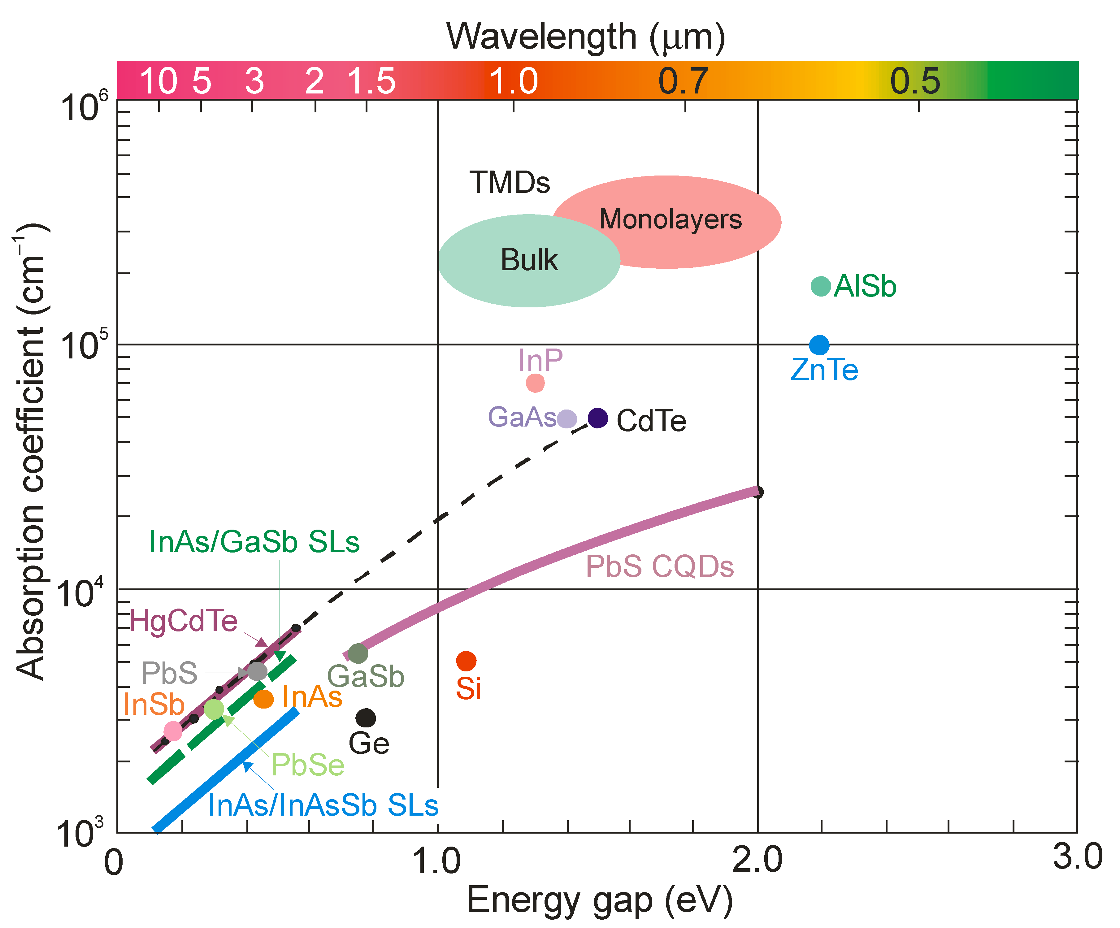
Figure 1 shows the absorption coefficient versus bandgap energy for different material systems at room temperature. The absorption coefficient was estimated for the threshold energy of 1.2 × Eg, where Eg is the semiconductor bandgap. For HgCdTe, the experimental data were taken from the work by Chu et al. [4]. The relationships presented for superlattices should be treated as approximate, due to some literature discrepancies. In general, the absorption coefficient for a superlattice is lower than for HgCdTe for a given bandgap energy. Moreover, the absorption coefficient of an InAs/InAsSb type-II superlattice (T2SL) is approximately half that of an InAs/GaSb superlattice at λ = 8 μm [5]. The same ratio was adopted for other wavelengths. Numerical modeling by Klipstein et al. [6] also confirmed the weaker coefficient of Ga-free superlattices.
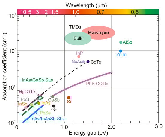
Figure 1.
Absorption coefficient versus bandgap energy for selected semiconductor materials at room temperature. Data for HgCdTe are taken from Ref. [4]. The transition metal dichalcogenides (TMDs) (both bulk and monolayers) of Mo and W are taken after Ref. [7]. The relationship α(E) for PbS CQDs is assumed from data taken from a number of papers.
Two-dimensional materials are derived from layered solids, in which atoms are linked together by ionic or tight covalent bonds in the 2D plane, while each of these atomic planes is bonded together by weak van der Waals (vdW) interactions along the out-of-plane direction. This atomic arrangement means that many 2D materials can be mechanically exfoliated from layered vdW solids. Furthermore, due to the weak physical bonds between individual atomic planes, it is possible to combine different 2D materials, along with the possibility of the arbitrary formation of heterostructures.
Although layered materials are made of the same atoms as their bulk counterparts, their band structures differ from each other. For example, in the case of transition metal dichalcogenides (TMDs), such as MoS2, MoSe2, WS2 and WSe2, the bandgap can be tuned by varying the number of layers—from a smaller indirect transition to a larger direct transition due to quantum confinement effects. Therefore, thanks to the tunable bandgap, TMDs can detect light of different wavelengths. In addition, the optical and electronic properties of these materials are strongly modified by the large strains.
Based on the data collected in Ref. [8], the most important conclusions regarding the absorption coefficients of TMDs and HgCdTe are as follows:
- the absorption coefficients of HgCdTe (Eg ≈ 0.1–0.3 eV) are below 104 cm−1 and for TMDs (Eg > 1 eV) above 105 cm−1, and
- for a hypothetical TMD with an energy gap of 0.1–0.2 eV, the abortion coefficient can be expected to be below 105 cm−1.
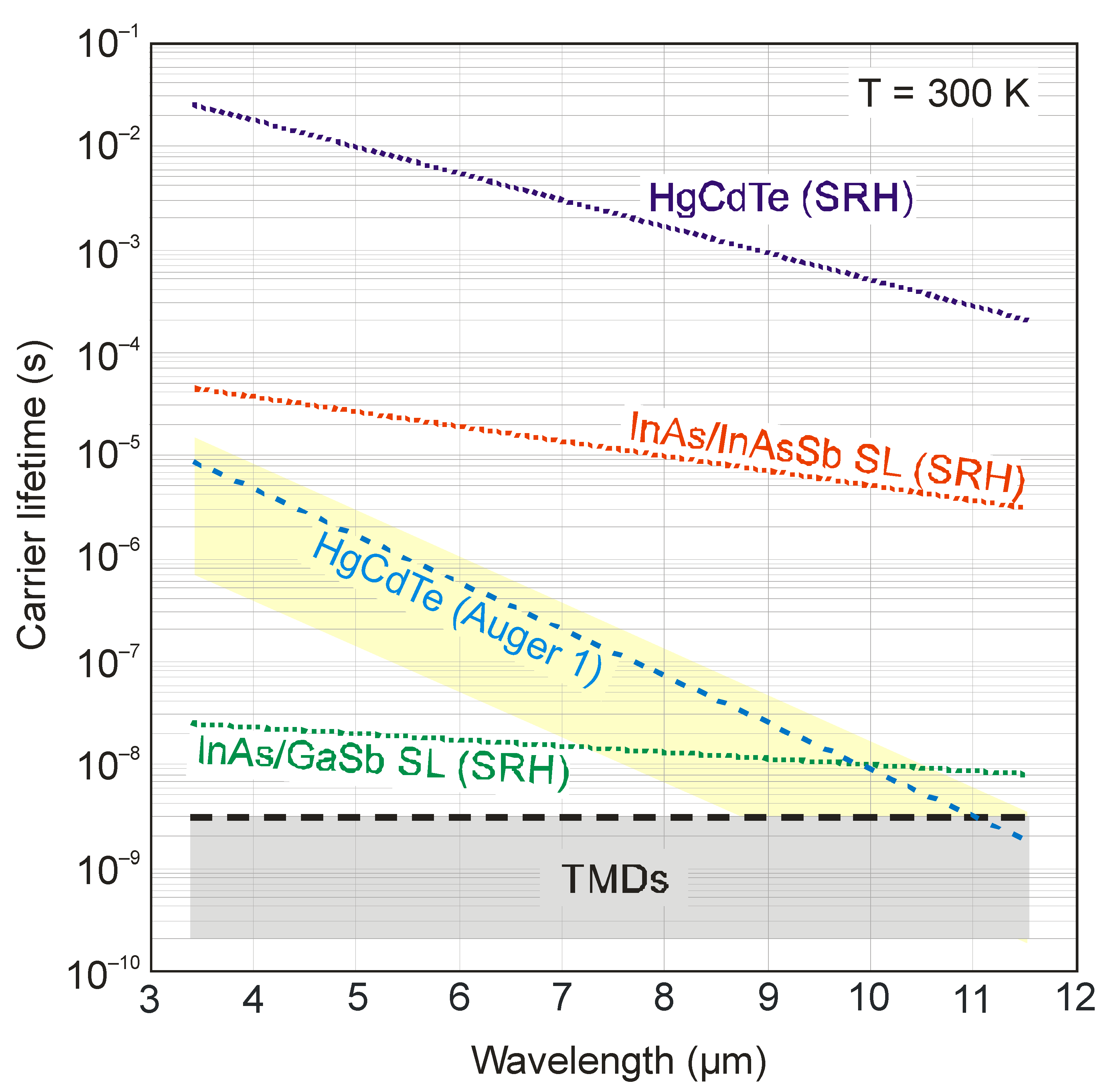
Figure 2 shows the minority carrier lifetime versus cut-off wavelength for different material systems at room temperature [9,10,11]. Among the presented materials, HgCdTe is characterized by favorable internal recombination mechanisms, which determine the long carrier lifetime and favor the operation of photodetectors in HOT conditions. The carrier lifetime of a lightly doped HgCdTe (~1013 cm−3) is specified by the Shockley–Read–Hall (SRH) mechanism. As is shown in Ref. [12], the highest reported values are 10 ms and 0.5 ms for a mid-wave infrared (MWIR) and a long-wave infrared (LWIR) absorber, respectively. These values were determined from the photodiode dark currents at low temperatures. Estimated lifetimes can be taken for photodetectors operating at room temperature [11]. Nevertheless, it should be noted that at 300 K, due to the high intrinsic carrier concentration (6 × 1015 cm−3 at MWIR, and 5 × 1016 cm−3 at LWIR range), the minority carrier lifetime is limited by Auger mechanisms—Auger 1 in the n-type and Auger 7 in the p-type material. The typical relation between intrinsic Auger 1 and Auger 7 lifetimes in HgCdTe is τAi7 ≈ 6τAi1 [11].

Figure 2.
Trend lines of collected minority carrier lifetimes in four material systems: HgCdTe, InAs/GaSb T2SLs, InAs/InAsSb T2SLs and TMDs. The highest line refers to the best HgCdTe data for the lowest doping level in the active photodiode region of ~1013 cm−3 [12]. The trends for Auger mechanisms were calculated for HgCdTe and refer to the intrinsic concentration, assuming |F1F2| = 0.15. In other semiconductors, the carrier lifetime limited by Auger mechanisms may be different depending on the ratio of the effective masses and the overlap integral |F1F2|. The possible range is marked with a yellow background.
An unknown mechanism creates SRH centers in semiconductors, involving residual impurities and native defects. In general, AIIIBV compounds exhibit more active SRH centers in comparison with AIIBVI ones including HgCdTe, resulting in lower minority carrier lifetimes. For example, the InAs/GaSb T2SL carrier lifetime limited by the SRH mechanism is typically several tens of nanoseconds, both in MWIR and LWIR absorbers. It is believed that the short lifetime is due to the presence of a shallow state near the GaSb valence band, which falls directly within the bandgap of InAs/GaSb SLSs. Ga-free InAs/InAsSb superlattices exhibit longer lifetimes, up to several microseconds for the MWIR region. In Ref. [13], the SRH lifetimes were determined from dark currents for the best InAs/InAsSb T2SL detectors. The obtained value for the MWIR absorber was 25 μs, and that for the LWIR absorber was 5 μs.
However, compared to a low-doped HgCdTe, SRH carrier lifetimes of InAs/InAsSb T2SL are up to three orders of magnitude lower for a similar bandgap. It is presumed that the SRH recombination mechanism is related to some semiconductors’ deviation from ideal crystallinity. In AIIBVI alloys, the ionic bonds are stronger than in the corresponding AIIIBV materials. For this reason, the electron wave function around the lattice sites is much more strongly compact, making the crystal lattices of AIIBVI compounds less prone to the formation of band states due to crystal imperfection [11].
Table 1 presents the estimated figures of merit for HgCdTe, InAs/GaSb and Ga-free InAs/InAsSb superlattices. It should be noted here that at 300 K, the highest reported values of the carrier lifetimes limited by the SRH mechanism can be obtained only with the appropriate detector design, in which the intrinsically generated carriers will be reduced to at least the doping level, or, as in the case of the HgCdTe P-i-N photodiode, to the complete depletion of the absorber. Between the two types of T2SLs, the difference in the values is an order of magnitude at LWIR and two orders of magnitude at the MWIR range. A better superlattice system has still a lower value compared to HgCdTe. This difference is mainly due to the much longer carrier lifetime in HgCdTe, as discussed above.

Table 1.
figures of merit for three sets of material systems at room temperature (after Ref. [3]).
Regarding Figure 2, the demonstrated carrier lifetime in two-dimensional materials is at the nanosecond level and is approximately five orders of magnitude lower than for the HgCdTe ternary alloy. The dominant recombination pathway for TMDs (MoS2, MoSe2 and WSe2) is exciton recombination [14,15,16]. Considering the experimental data collected above for LWIR HgCdTe (α = 2.2 × 103 cm−1, τ = 0.5 ms) and TMDs (α = 2 × 105 cm−1, τ = 1 ns), it is also interesting to compare the estimated values for these two material systems. For HgCdTe, is equal to 1.05 (s/cm)1/2, while, for TMD materials, it is 1.4 × 10⁻² (s/cm)1/2, which is two orders of magnitude smaller. However, this is a value close to the one predicted for InAs/InAsSb T2SL. It should be noted that the value of was compared for semiconductors with significantly different bandgaps. The absorption coefficient for TMDs was taken for an energy gap on the order of 1 eV, while, for HgCdTe, it was 0.1 eV. For a hypothetical 2D material with a narrow energy gap (0.1 eV, as is the case of HgCdTe), the absorption coefficient should be smaller (by approximately one order of magnitude), which would result in an even smaller value compared to HgCdTe.
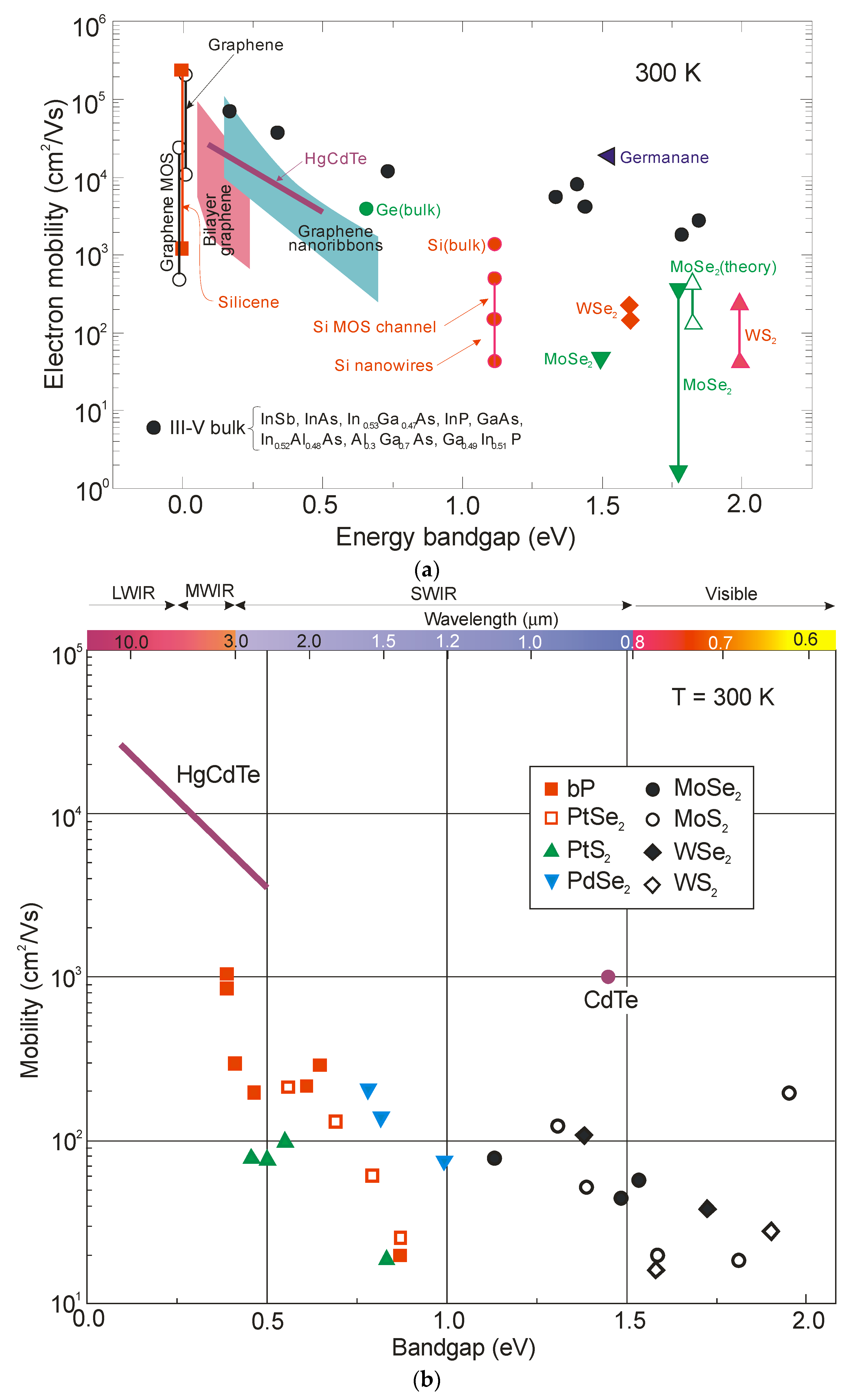
Considering electron mobilities, TMD 2D materials do not show a distinct advantage over the conventional 3D bulk materials. Figure 3 compares the electron mobilities for selected materials, namely group-6 TMDCs, black phosphorus (bP) and typical noble TMDs on a back-gated SiO2 substrate, with the standard bulk semiconductors used in IR detector (HgCdTe and AIIIBV alloys) production.
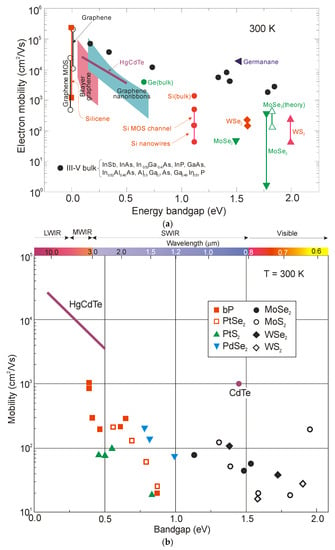
Figure 3.
Comparison of room-temperature electron mobilities of selected layered material systems with standard semiconductors used in IR detector fabrication: (a) comparison with AIIIBV compounds and HgCdTe ternary alloy; (b) electron mobility of HgCdTe (after Ref. [17]) and layer-dependent mobilities of group-6 TMDCs, bP and typical noble TMDs on back-gated SiO2 substrate (after Ref. [8]). Other experimental data come from various sources.
3. Ultimate HgCdTe Photodiode Performance
For more than 60 years, since 1959, when HgCdTe was discovered [18], this material system has successfully overcome the major challenges of different types of detector families, including extrinsic silicon, Schottky barriers on silicon, lead–tin telluride devices, AlGaAs multiple quantum wells, T2SL and especially silicon microbolometers. This leads to the following question: will the further development of 2D materials affect the privileged position of HgCdTe?
In the literature, it has been accepted to compare the performance of different types of IR detectors with developed rules for HgCdTe, such as Rule 07 [19] and Rule 22 (an update of Rule 07) [20], as well as Law 19 [12]. Thus far, Rule 07 has become very common among the IR community as a reference technology. Since the first two rules are empirically derived standards for p-on-n HgCdTe photodiodes constrained by the Auger 1 mechanism due to an extrinsic doping concentration in the active region of ~1015 cm−3 for Rule 07 and <1015 cm−3 for Rule 22, it is expected that for a very low-doping active region (around 1013 cm−3), the values of the photodiode dark current density can be lower. However, this is not the case for Law 19 due to the fact that it is a relationship determined by a fundamental law—the dark current density is limited by the background radiation from the surrounding environment reaching the detector. This current is crucial because it is not due to imperfections in the material, detector design or associated electronics, but rather to the detection process itself, which is determined by the discrete nature of the radiation field.
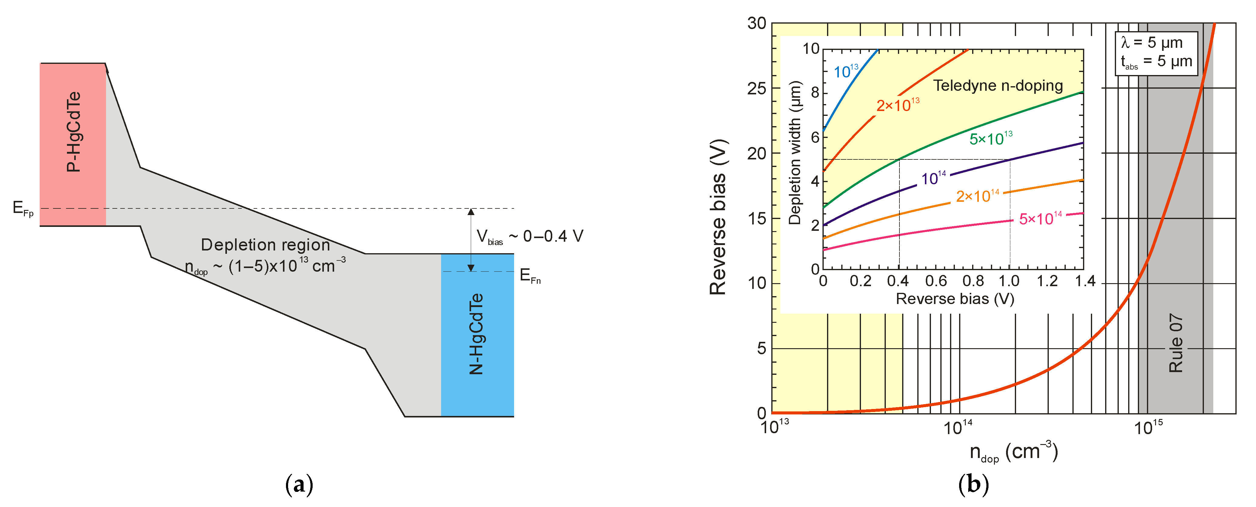
Figure 4 presents the optimal P-i-N HOT photodiode structure with a very low doping concentration of approximately 1013 cm−3 in the active i-region. The wide gap regions surrounding the absorber (cap P-type contact layer and N-type buffer) act as barriers, reducing the dark current in the absorber and not contributing to it themselves, and they prevent a tunnelling current under reverse bias. The i-active region can be completely depleted depending on the doping concentration and reverse voltage. At the doping range of approximately 1015 cm−3 (which includes Rule 07), the 5-μm-thick MWIR absorber is completely depleted by applying a relatively high reverse voltage between 10 V and 30 V—see Figure 4b. Similar relationships exist for LWIR photodiodes. However, for the doping range recently achieved in Teledyne (from 5 × 10¹³ to 1 × 1013 cm−3), the fully depleted i-region is reached for a reverse bias from 0.4 up to zero volts, respectively. This range of reverse polarization of photodiodes is typically used to read the signal through the ROIC in the array pixel.
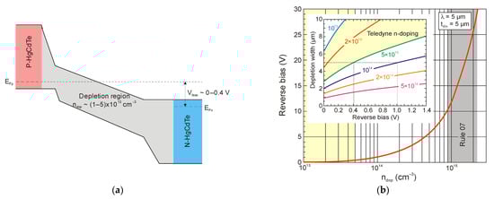
Figure 4.
Schematic energy band diagram of a reverse-biased P-i-N HgCdTe photodiode (a) and calculated reverse bias voltage versus doping concentration required to deplete a 5-μm-thick MWIR HgCdTe absorber (b). Inset: depletion width versus reverse bias voltage calculated for selected doping concentration.
For a fully depleted P-i-N photodiode, the dark current density can be calculated from the expression
where tdep is the depletion region width. The depletion dark current exhibits a temperature dependence given by ni.
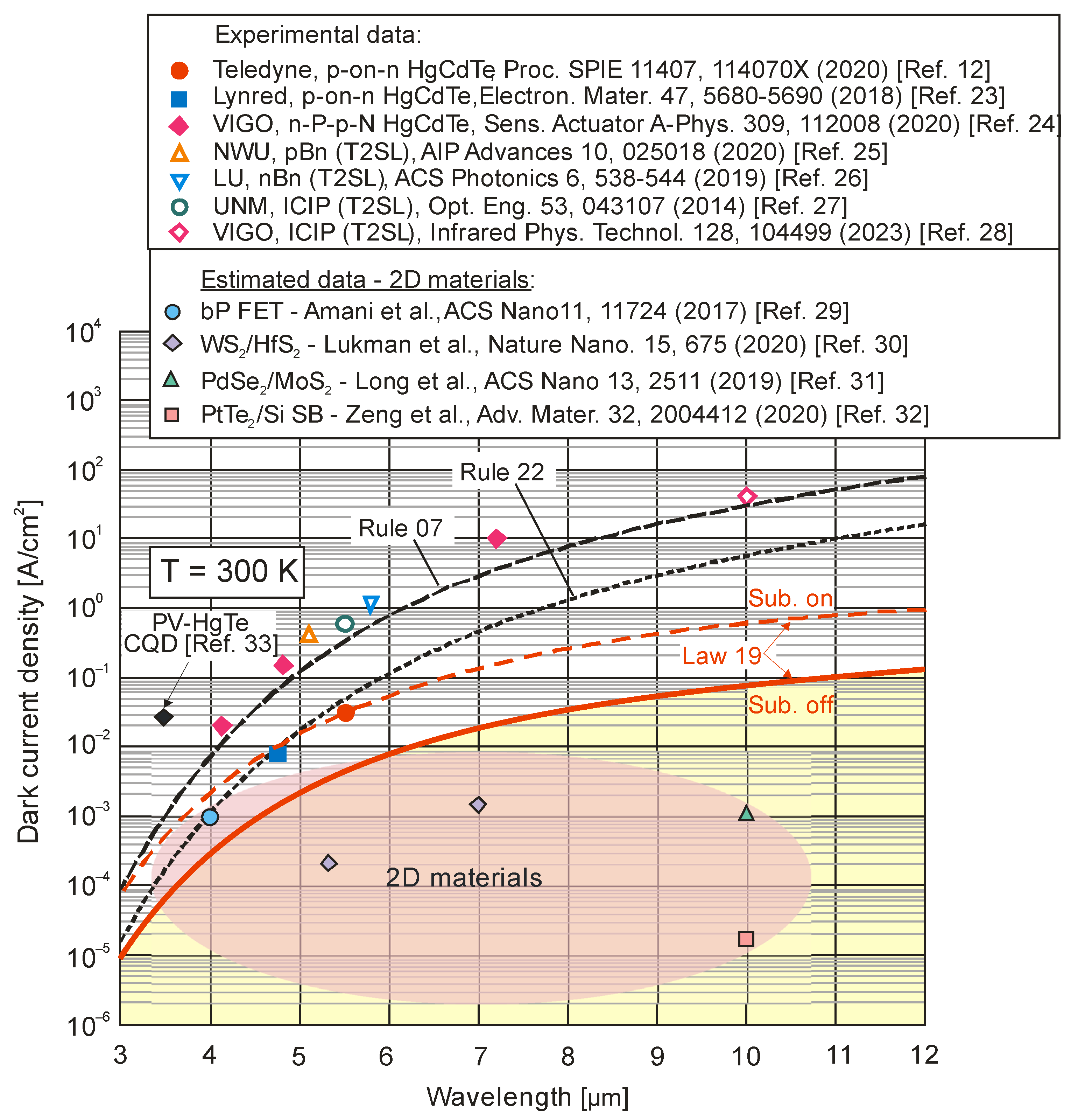
Figure 5 summarizes the dark current densities of selected IR detectors operating at 300 K. In addition, the curves defined by Rule 07, Law 19 and Rule 22 are marked for comparison purposes. The curve marked “substrate-off” corresponds only to the background radiation limit, while “substrate-on” is also due to the device design. The “substrate-on” radiation limit is increased by the square of the substrate refractive index—for CdZnTe, it is a factor of 7.3. The total background radiation incident on the detector is increased due to the reflection of radiation (emitted from the neutral regions of the p-and-N photodiode) from the substrate–air interface [12,13].
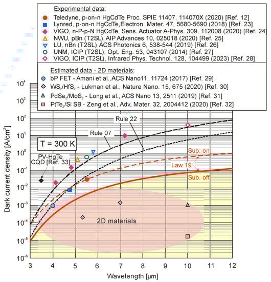
Figure 5.
Published dark current density data for selected IR photodetectors at 300 K, compared with HgCdTe Rule 07, Rule 22 and Law 19. Experimental data are gathered for p-on-n [12,21] and N-P-p-N HgCdTe [22] photodiodes and T2SL (barrier and cascade) photodetectors [23,24,25,26]. The lowest current densities are marked for photodetectors made of 2D materials. The current density values for the latter are estimated from the data in the respective papers [27,28,29,30]. Moreover, the dark current density for an MWIR CQD HgTe photodiode is marked [31].
As shown in Figure 5, Teledyne and Lynred have fabricated fully depleted photodiodes that operate at the “substrate-on” radiative limit in the MWIR spectral range. The removal of the substrate provides a further opportunity to improve the detector performance. The BLIP performance has the greatest impact on the current density for photodiodes operating in the LWIR region, while, for the SWIR region, the advantage in using fully depleted devices is very small from a dark current perspective.
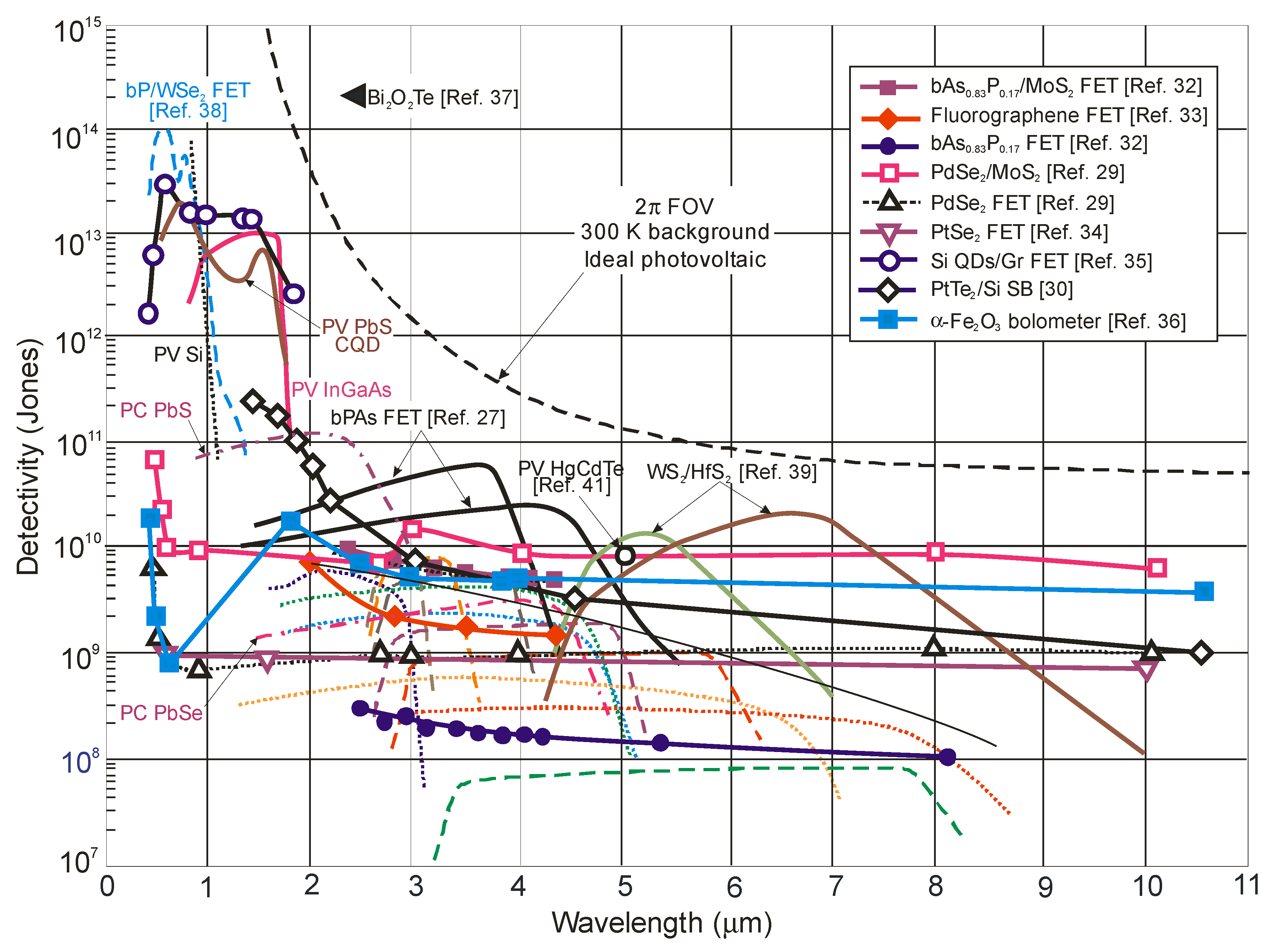
Figure 6 collects the spectral detectivities published in the literature for different groups of single-element IR photodetectors operating at room temperature, including those fabricated from low-dimensional solids such as 2D materials. The performance of standard photodetectors made of HgCdTe, T2SLs, lead chalcogenides (PbS and PbSe) and InGaAs is sub-BLIP. It is interesting to note that the performance of T2SL-based interband quantum cascade infrared photodetectors (IB QCIPs) is comparable to HgCdTe. As shown in Section 2, the adoption of the α/Gth standard indicates theoretically the superior performance of HgCdTe photodiodes compared to 2D material photodetectors. However, the literature data collected in Figure 6 for 2D photodetectors contradict this conclusion, with more considerations given in Section 5.
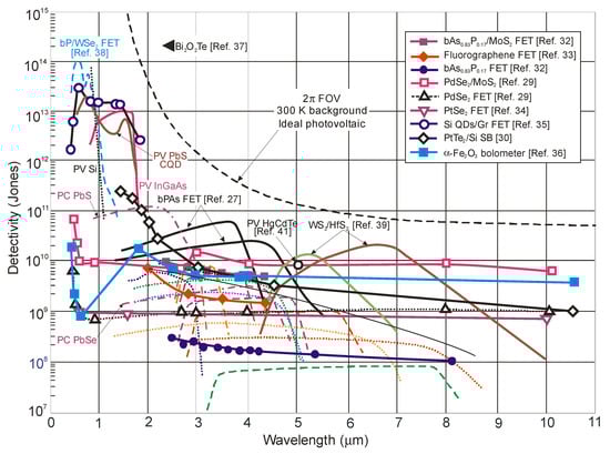
Figure 6.
Room-temperature spectral detectivity curves for selected 2D material photodetectors [27,29,30,32,33,34,35,36,37,38,39] and the commercially available photodetectors (PV-Si and PV-InGaAs, PC-PbS and PC-PbSe, HgCdTe photodiodes (dashed lines—Ref. [40], and Ref. [41])). The spectral detectivity curves of T2SL IB QCIPs are marked by dotted lines (Ref. [42]). PC—photoconductor, PV—photodiode, FET—field effect transistor.
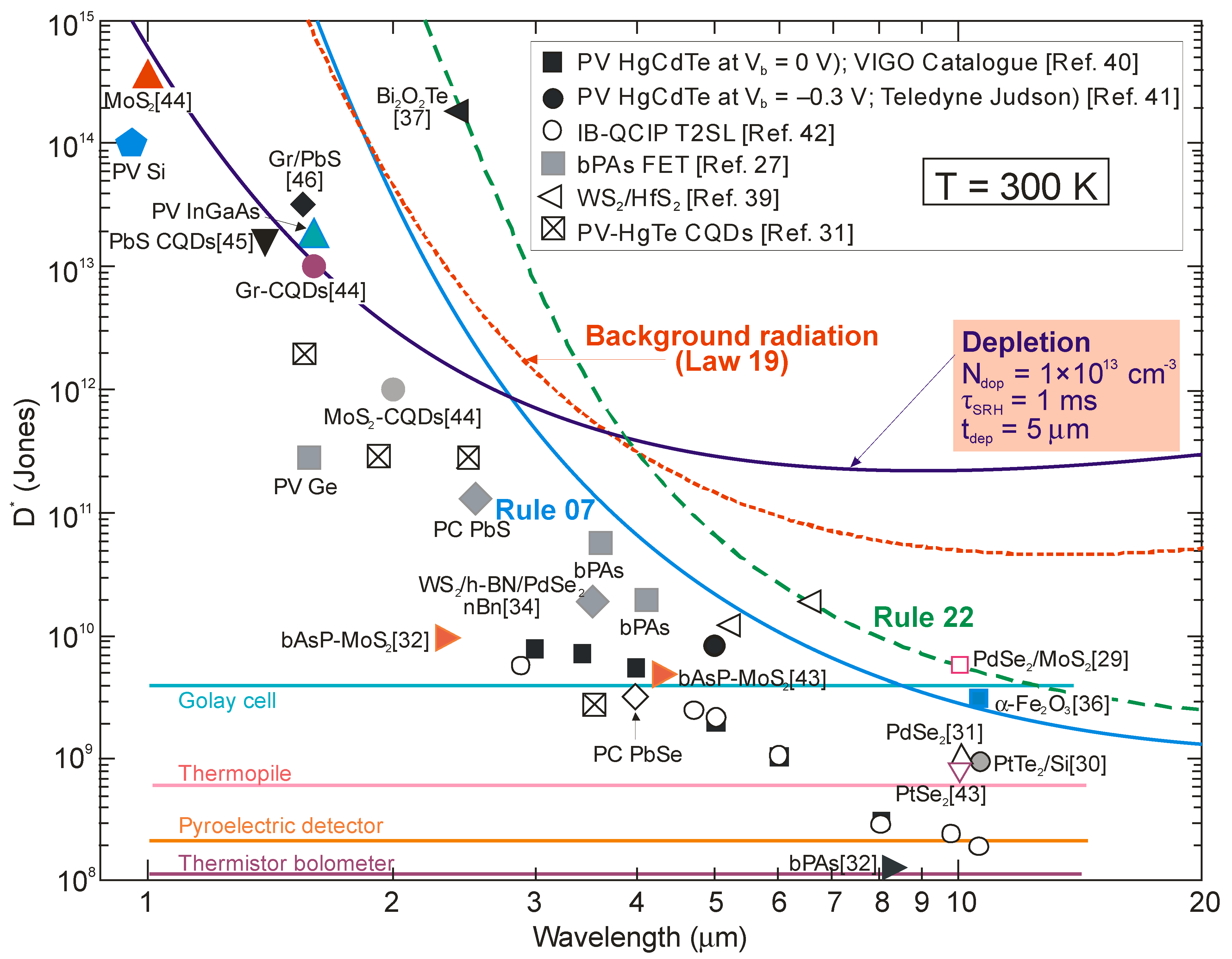
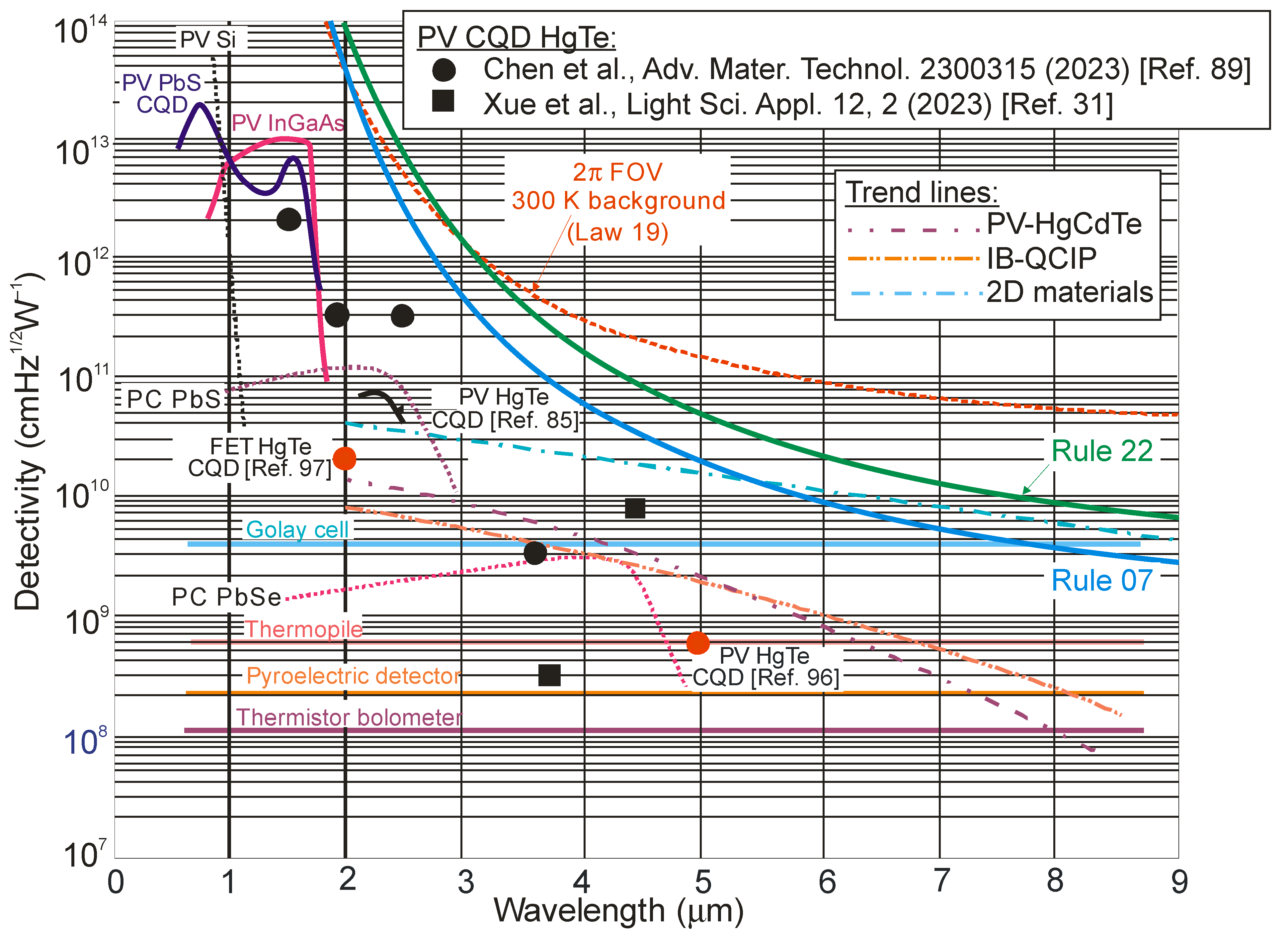
Figure 7 shows the current performance of HOT photodetectors and at the same time indicates future possible further development. At the current stage of HgCdTe technology development, the semi-empirical Rule 07 does not meet the original assumptions [12,43]. At this point, it should be noted that this metric is closely related to the p-on-n photodiode limited by the Auger 1 mechanism due to an extrinsic doping concentration in the active region of ~1015 cm−3. Figure 7 shows that, according to Law 19, the detectivity of P-i-N HgCdTe photodiodes with doping at the level of 1 × 1013 cm−3, operating at room temperature in the spectral range above 3 μm, is limited by background radiation (with a D* level above 1010 Jones) and can be improved by more than one order of magnitude compared to Rule 07 predictions in the LWIR spectral region. Among the material systems used in HOT LWIR photodetector fabrication, only HgCdTe meets the expectations required to achieve the BLIP conditions: low doping at the level of 1013 cm−3 and a high SRH carrier lifetime in the 1 ms range.
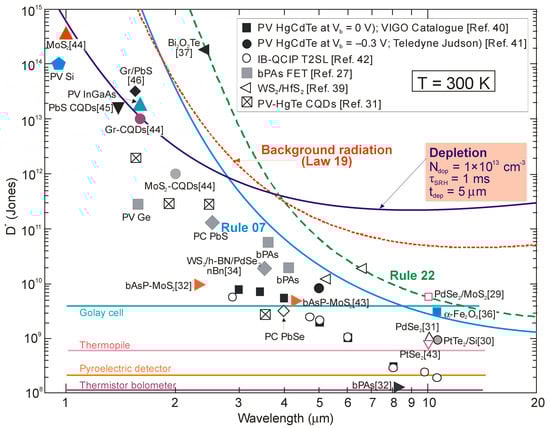
Figure 7.
Room-temperature spectral detectivity data for commercially available IR photodetectors (PV-Si and PV-Ge, PV-InGaAs, PC-PbS and PC-PbSe, PV-HgCdTe [40,41]). Experimental data for IB QCIPs based on T2SLs [42], selected 2D materials [27,29,30,32,34,36,37,43,44,45,46] and CQD [31]. Theoretical calculations (curve labeled as “Depletion”) are for P-i-N HOT HgCdTe photodiodes assuming τSRH = 1 ms, absorber doping level of 1 × 1013 cm−3 and active region thickness t = 5 μm. Also marked for comparison are the curves defined by Rule 07 and Rule 22. PC—photoconductor, PV—photodiode, FET—field effect transistors. Typical detectivity values of thermal detectors (thermistor bolometer, pyroelectric detector, thermopile and Golay cell) are also marked for comparison purposes.
4. Interband Quantum Cascade Infrared Photodetectors (IB QCIPs)
As is commonly known, the responsivity of conventional photodiodes is closely related to the diffusion length, and increasing the absorber thickness well beyond the diffusion length no longer gives the desired improvement in the signal-to-noise (S/N) ratio. In other words, when the absorption depth is longer than the diffusion length, as for HgCdTe photodiodes operating in the LWIR spectral range, only a limited fraction of the photogenerated charge carriers contribute to the quantum efficiency (QE). Especially at high temperatures, where the diffusion length is usually reduced, this effect is most pronounced.
To circumvent the limitations of the reduced diffusion length, new detector designs such as intersubband (IS) ambipolar quantum cascade photodetectors (IS QCIPs), derived from quantum well infrared photodetectors (QWIP) and quantum cascade lasers (QCL), were introduced in the early 2000s to effectively increase the absorption efficiency [47]. The distinguishing feature of this type of photodetector is that they can be implemented in chemically stable material systems with well-established epitaxial growth, such as molecular beam epitaxy (MBE), and device processing technologies. Most IS transition-based devices are fabricated based on AIIIBV materials: GaAs QWs with AlGaAs-matched barriers or InGaAs QWs with AlInAs-matched barriers. They are also characterized by better uniformity and a lower surface leakage current.
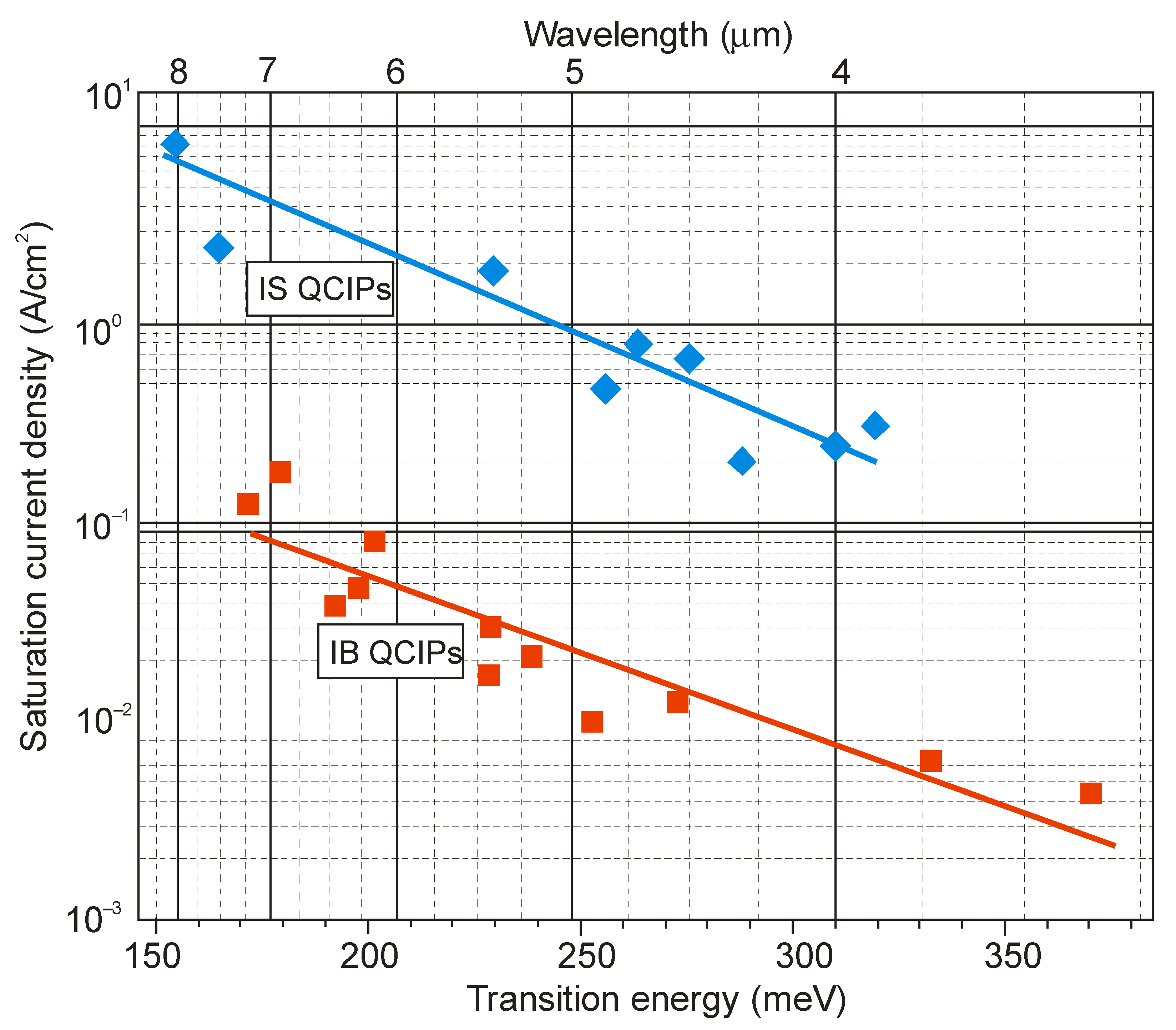
However, in the last decade, it has been shown that interband (IB) unipolar QCIPs based on type-II AIIIBV superlattices are more effective devices. The performance of IB QCIPs is higher than that of IS QCIP ones, mainly due to the much longer carrier lifetime, which translates into two orders of magnitude lower saturation current densities for IB QCIPs than reached for IS QCIPs—see Figure 8.
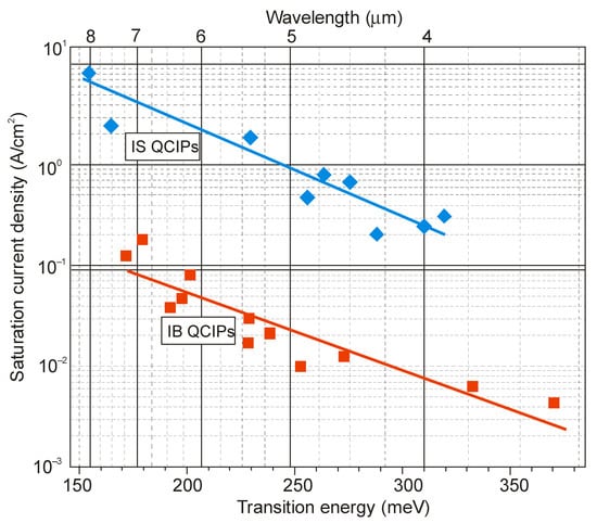
Figure 8.
Room-temperature saturation current density of IS and IB QCIPs (adapted after Ref. [48]).
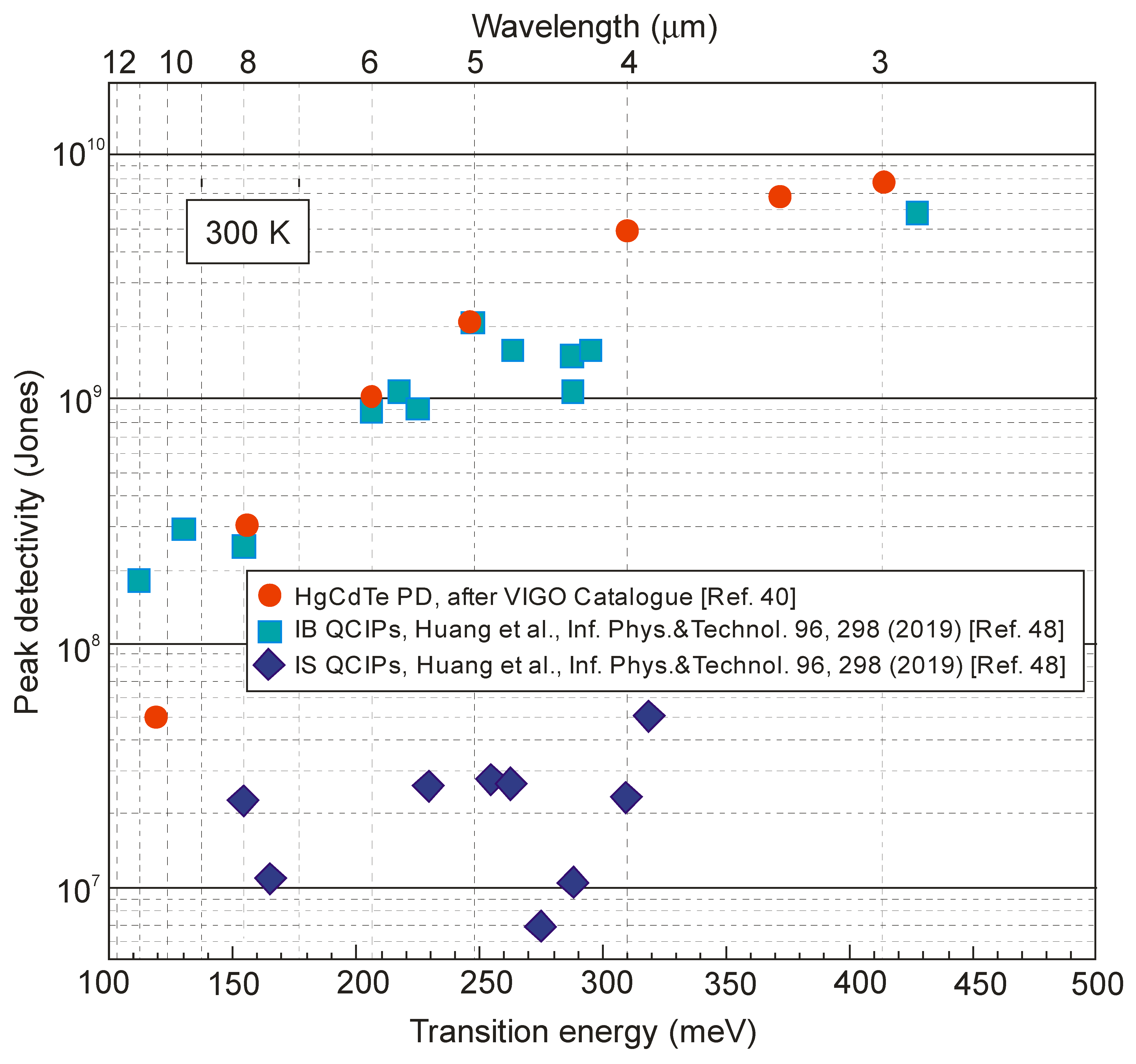
Figure 9 compares the estimated peak detectivities limited by Johnson noise (based on the measured R0A product and responsivity at zero bias) for both types of QCIPs with commercially available HgCdTe photovoltaic detectors. It is clearly shown that the performance of IB QCIPs is comparable to that of HgCdTe. An additional advantage of QCIPs is that, thanks to the strong covalent bonds of AIIIBV semiconductors, they can operate at temperatures up to 350 °C, which is not possible for the HgCdTe counterpart. However, the sophisticated structures of IB QCPs, with many interfaces and strained thin layers, are the main problem in technology development, also due to increased production costs. Thus far, attempts to obtain a high-quality infrared detector array with IB QCIPs pixels are not very optimistic. The minimum noise equivalent difference temperature (NEDT) of 28 mK at a long integration time (up to 30 ms) was obtained at 120 K with f/2.3 optics using a 320 × 240 focal plane array (pixel size of 24 × 24 μm2) and standard commercial read-out circuit technology [49]. In the longer term, however, the flexibility of structure designs and material parameters provides tremendous scope for improvements in their performance.
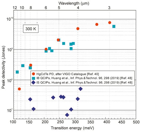
Figure 9.
Room-temperature peak detectivity versus transition energy and wavelength for IB and IS QCIPs (Ref. [48]), compared with commercial HgCdTe photodiodes (Ref. [40]).
5. Two-Dimensional Material Infrared Photodetectors
Two-dimensional materials are promising candidates for high-performance photodetectors operating over a wide spectral range, due to novel and unusual properties such as the following:
- the electronic states, with a typical thickness of less than 10 nm, are easily tuned by external fields (e.g., ferroelectric field, gate-induced electrostatic field and photogating localized field);
- their bandgaps, ranging from 0 eV for graphene up to 6 eV for hexagonal boron nitride (h-BN), make it possible to produce photodetectors that operate from ultraviolet (UV) up to far IR or even terahertz (THz);
- the bandgaps are closely related to the number of layers—increasing the number of layers, the band gap is reduced;
- for some TMDs, such as MoS2, MoSe2, WS2 and WSe2, monolayers are direct bandgap semiconductors, while the bulk materials are indirect bandgap semiconductors.
Due to the fact that there is no need to pay attention to the lattice matching, as in conventional semiconductors, the random stacking and fabrication of 2D material devices is a tremendous advantage. A stack of atomic planes placed on top of each other, held together by vdW forces, leaves no dangling bonds, which promotes the fabrication of vertical heterostructure devices. Additionally, the weak vdW interactions allow the development of 2D materials on a large scale, regardless of the substrate, and the integration of 2D materials into silicon chips, which represents huge potential in the production of electronic and optoelectronic devices.
At the present stage of technology, however, the following issues influence the development of 2D material photodetectors:
- they are susceptible to absorbates owing to their atomic thicknesses, defects and doping;
- they lag significantly behind the traditional infrared material technologies, including low-quality heterojunctions between the monolayers of vertically stacked TMDs;
- they do not show a distinct advantage over the conventional 3D bulk materials and, in addition, the carrier mobility varies along different crystal orientations (in consequence, the design of devices along the preferred direction is crucial for high responsivity and a short time constant);
- their performance, in the majority of cases, is dictated by the nature of layer stacking (twist, spacing, etc.) and their environment (strain, pressure, etc.);
- despite the large absorption coefficient, the atomically thin materials are not applicable for intense light, which leads to a poor linear dynamic range.
Despite the mentioned drawbacks, a new class of materials (2D materials and quantum dots/nanowires) can compete with standard commercial photodetectors. Many papers have been published on this topic; some of them are overly enthusiastic.
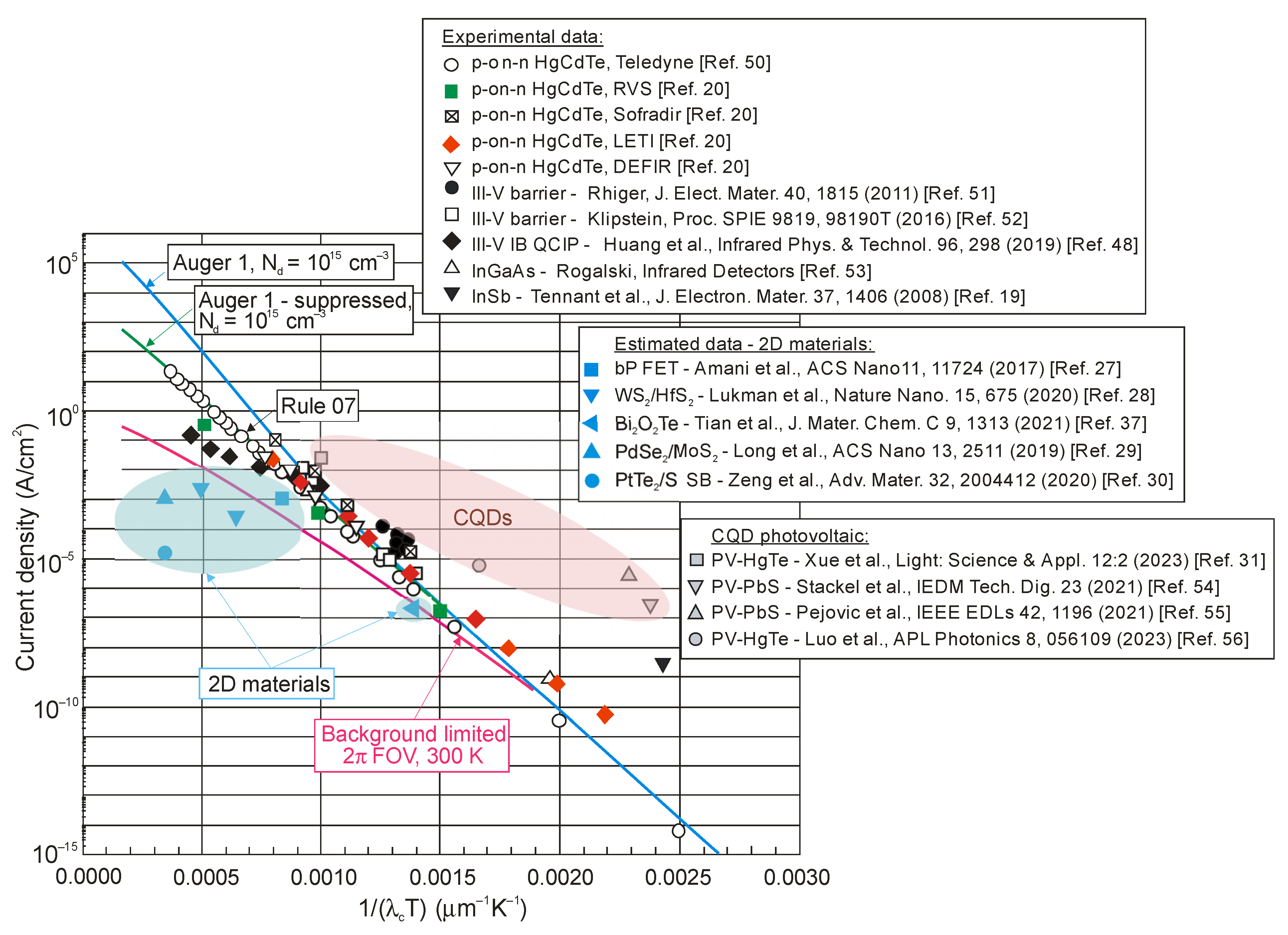
Figure 5 shows that the estimated dark current densities for 2D material photodetectors selected from the literature represent the record/lowest values to date for photodetectors operating at room temperature. Figure 6 and Figure 7, on the other hand, show published higher detectivities of 2D layered photodetectors compared to commercially available standard detectors, including photodiodes with HgCdTe. The available literature describes photodetector performance that exceeds the physical limit—limited by the influence of background radiation. This is best seen in Figure 5 and Figure 10. This second figure collects the experimental dark current densities, versus the reverse of the λcT product, of a wide group of photodetectors operating at 300 K. The red curve is theoretically calculated according to the Law 19 metric, i.e., it determines the dark current density resulting from the influence of background radiation at the 2π field of view (FOV) and 300 K. The highlighted values in Figure 10 were obtained from texts, tables or graphs included in the available publications. For photodetectors made of 2D materials, the dark current density is estimated based on available data in published papers.
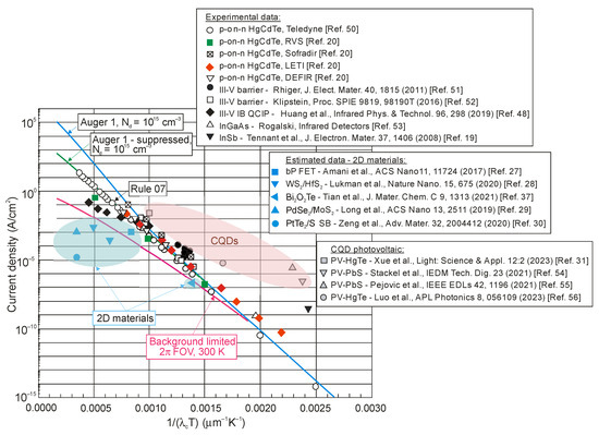
Figure 10.
p-on-n HgCdTe photodiodes’ current density versus 1/(λcT) product [50]. Experimental data are presented for p-on-n HgCdTe photodiodes [20,50] and alternative technologies [29,48,51,52,53] to include 2D materials [27,28,29,30,37] and CQDs [31,54,55,56]. The red curve is calculated theoretically according to Law 19 benchmark for 2π FOV and 300 K.
The authors of several published papers have underlined cases where the performance of 2D layered photodetectors is overestimated due to the lack of precisely defined procedures for their characterization [57,58,59,60]. As is shown in a recently published paper [60], the misinterpretation of layered photodetector performance is due to
- incorrect noise estimates;
- the miscalculation of the device active area and radiation power density;
- the contradictory bandwidth of measured responsivity and noise.
Both shot and generation-recombination (GR) noises depend on the photoconductive gain, g. The implementation of an incorrect shot noise expression () instead of ) leads to a false increase in the signal to noise (SNR) ratio by a factor of . The last equation shows that the shot noise calculation error rises for higher gains and is remarkably important for high-internal-gain photodetectors.
The development of a low-dimensional solid (LDS) photodetector requires proper characterization procedures consistent with those used for typical bulk-based photodetectors.
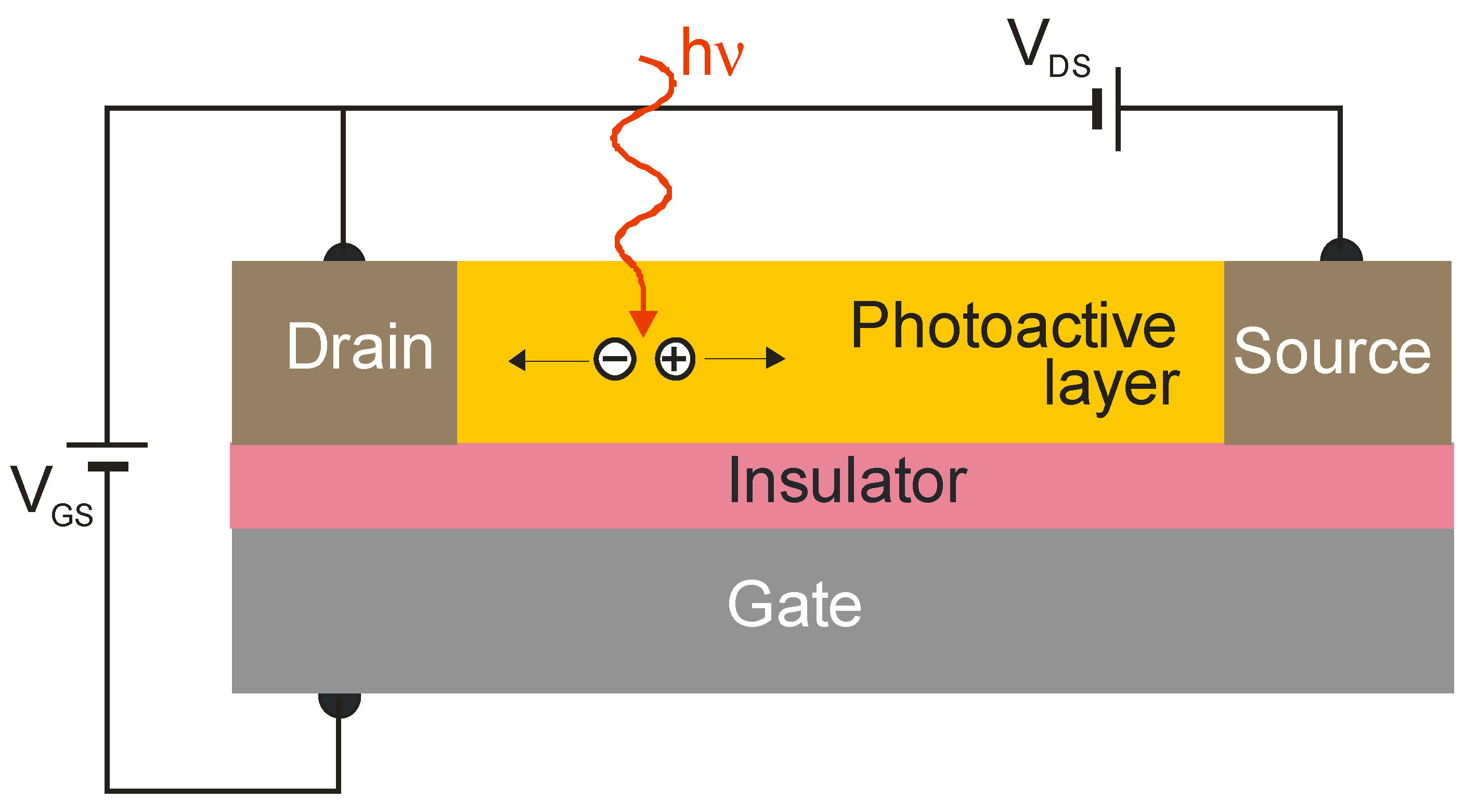
The highest-performance 2D material photodetectors are among phototransistors. Figure 11 explains how a phototransistor operates resembling a simple photoconductor, where the signal is caused by the generation of an electron–hole pair when one type of carrier is trapped by localized states (nanoparticles and defects). Typically, the photoconductive gain may be simply calculated by the ratio of the carrier lifetime to the transit time between the detector’s contacts. When the carrier’s drift length is greater than the contact distance, the charge swept from one electrode is instantly replaced by the injection of an equal free charge on the second contact, making the free charge circulate in the circuit until recombination, leading to signal amplification—a photoelectric gain. The phototransistor’s active region is separated from the substrate by an insulator, allowing the application of a gate voltage, VG, to control carrier transport in the active region. The active region was found to be more susceptible to the local electric field than typical bulk materials, and the optical generation can strongly modulate the conductivity of the channel by the external gate voltage, VG. Under such conditions, a much higher optical gain can be achieved. Generally, however, the gain in phototransistors can vary significantly versus the gate voltages due to the gate-controlled number of trap states.
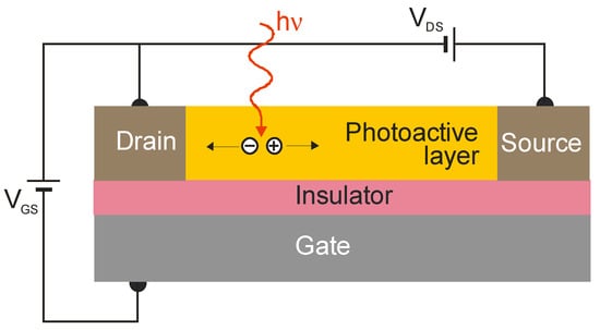
Figure 11.
Model of the phototransistor. A current signal is usually converted to a current mode amplifier.
Below, we will discuss the difference in dynamic behavior between conventional and layered IR photodetectors.
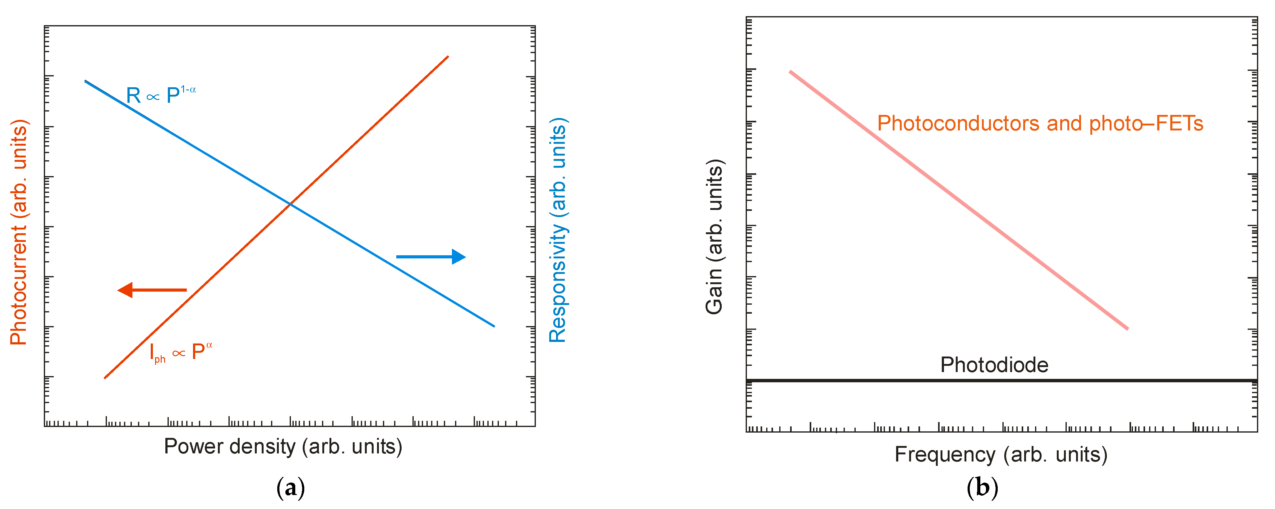
Practical applications require high-performance photodetectors characterized by a wide and linear dynamic range of operation, meaning that the photocurrent exhibits a linear dependence on the incident radiation power before absorption saturation. In this case, Iph α Pα, where α is close to 1. However, in the case of LDS photodetectors, including 2D material photodetectors, a nonunity exponent, 0 < α < 1, is often found, which is due to complicated carrier generation-recombination and trapping mechanisms. The responsivity is determined from the formula R = Iph/P, so R α P−(1−α). Figure 12a shows the net photocurrent and responsivity nonlinear radiation power dependence. If level of the incident radiation increases, the carriers are gradually captured, leading to complete trap filling and a decrease in the carrier lifetime and photoelectric gain. The gain in a photoconductor is proportional to the lifetime, while the response bandwidth is inversely proportional to the carrier lifetime. It follows that the gain × bandwidth product of the photoconductor is limited—see Figure 12b.
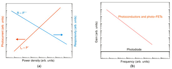
Figure 12.
Dynamic characteristics of photodetectors: (a) net photocurrent and responsivity radiation power dependence; (b) relationship between gain and frequency.
In the low-power range of incident radiation, the sensitivity is not influenced due to the high trap state density. In general, however, the sensitivity values published in the literature are not a criterion for the comparison of the quality of photodetectors, as they are measured for different incident radiation power densities. It has been assumed that to determine the current responsivity of photodetectors, it is common to use an incident radiation power density that is several orders of magnitude <1 mW/cm2 [61,62].
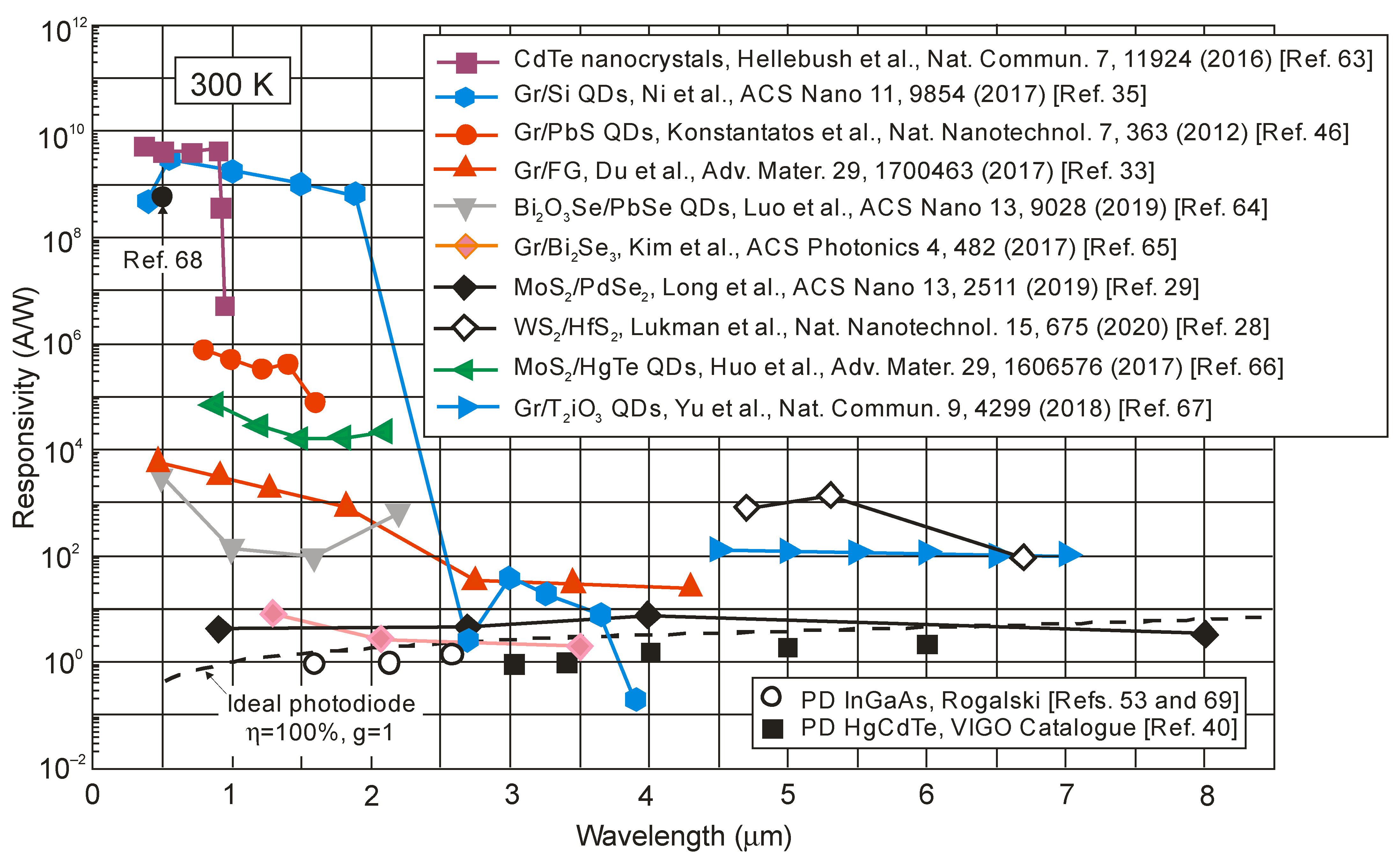
Figure 13 summarizes [28,29,33,35,46,63,64,65,66,67,68] the responsivity of selected LDS devices, including 2D material photodetectors, with current responsivity reaching ~1010 A/W and ultrahigh gain >109 electrons per photon, for the wavelength <2 μm. The InGaAs and HgCdTe photodiodes’ photoelectrical gain = 1, due to the separation of minority carriers by the electric field of the depletion region. For LDS photodetectors, the high-sensitivity detectors have a low response rate, being independent of the spectral range and being confirmed by the experimental data presented in Figure 14 (from visible (VIS), through SWIR and MWIR to LWIR). Response times of up to a few seconds are observed for LDS photodetectors in the visible range. This is a challenge in reaching both high photoresponsivity and a fast response simultaneously.
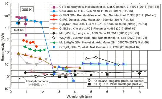
Figure 13.
Current responsivities of LDS IR photodetectors at 300 K [28,29,33,35,46,63,64,65,66,67,68]. The performance of HgCdTe [40] and InGaAs [53,69] commercially available photodiodes is presented along with the predicted theoretical curve.
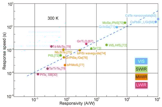
Figure 14.
Relationship between current responsivity and response speed for 2D photodetectors operating in broad IR spectral range at 300 K. Experimental data are taken from literature as labeled [30,63,68,70,71,72,73,74,75,76,77,78,79].
6. Colloidal Quantum Dot Infrared Photodetectors
Quantum dot (QD) photodetector development (with origins in the 1990s) has seen an evolution from epitaxially grown self-assembled QD detectors to a new generation of colloidal nanocrystal-based devices. A particular development in the latter has been observed in the last decade, where an active region is based on 3D semiconductor nanoparticles. CQDs offer a potential alternative to the InGaAs, InSb, InAsSb and HgCdTe as well as T2SLs in the SWIR and MWIR spectral regions. They are typically fabricated by conducting polymer/nanocrystal blends or nanocomposites. Nanocomposites are characterised by narrow bandgap energy, e.g., AIIBVI compounds (HgTe, HgSe) and AIVBVI compounds (PbS or PbSe). Table 2 summarizes the pros and cons of CQD devices.
Table 2.
Pros and cons of CQD IR devices.
Early studies of CQD-based detectors were reported for the NIR to MWIR photoconductors. Despite simplicity in device architectures, their performance was restricted by the dark currents, 1/f noise and problems in doping concentration monitoring.
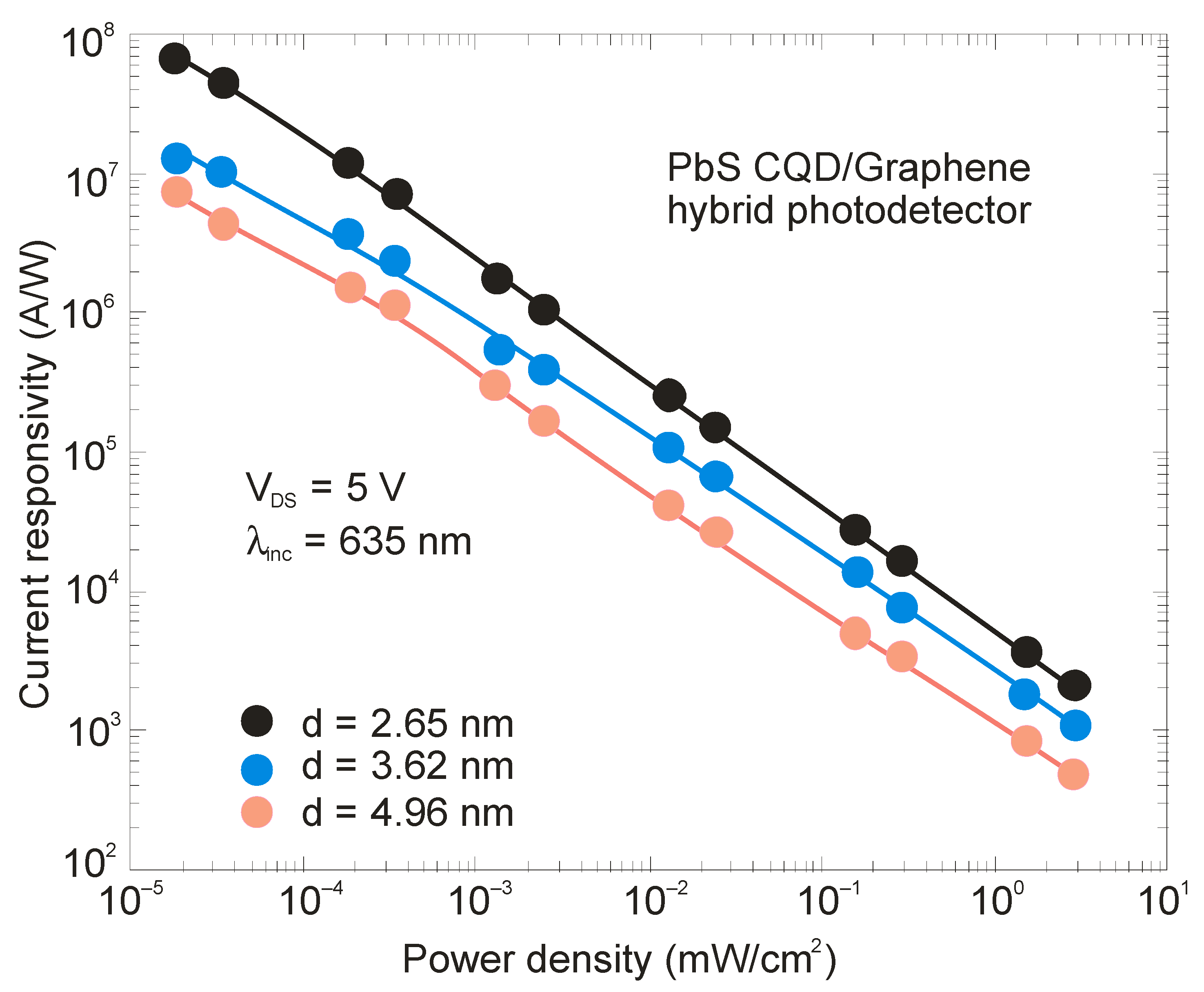
The responsivity of hybrid photodetectors (in fact, phototransistors—see Figure 11) can be considerably higher than commercially available detectors; however, a significant decrease in response time (bandwidth) is visible. The majority of these detectors exhibit a reduced linear dynamic range conditioned by the charge relaxation time (see Figure 12), leading to a decrease in responsivity versus radiation power. Figure 15 presents the current responsivity versus radiation intensity for a hybrid PbS/graphene QD photodetector with selected QD sizes [80]. This figure also shows the responsivity dependence on the QD size. For small QDs (d = 2.65 nm), the responsivity reaches >107 A/W for low radiation power. Typically, the response time (millisecond range and longer) is three orders of magnitude longer than commercially available detectors (microsecond range and shorter). The recovery process exhibits a slow component > 1 s connected with traps in the QDs [46]. The presented drawbacks restrict potential applications. The high current responsivity of the hybrid detectors is determined by the high photoelectric gain. As this gain also increases shot noise and g-r noise, this does not usually translate into higher detectivity.

Figure 15.
Current responsivity versus radiation power density for hybrid PbS QD/graphene device for selected QD size (adapted after Ref. [80]).
One other point should be borne in mind in the context of FPA fabrication. The hybrid detector needs a three contact device (like a phototransistor), affecting the FPA’s power consumption and limiting the fill factor. Moreover, the hybrid pixels’ complicated design influences FPAs’ uniformity and operability, and QDs’ nonuniformity considerably restricts the performance [81].
Current research is directed towards CQD photovoltaic devices with lower 1/f noise and dark currents. Thus, our attention will be focused towards photodiodes with more sophisticated structures.
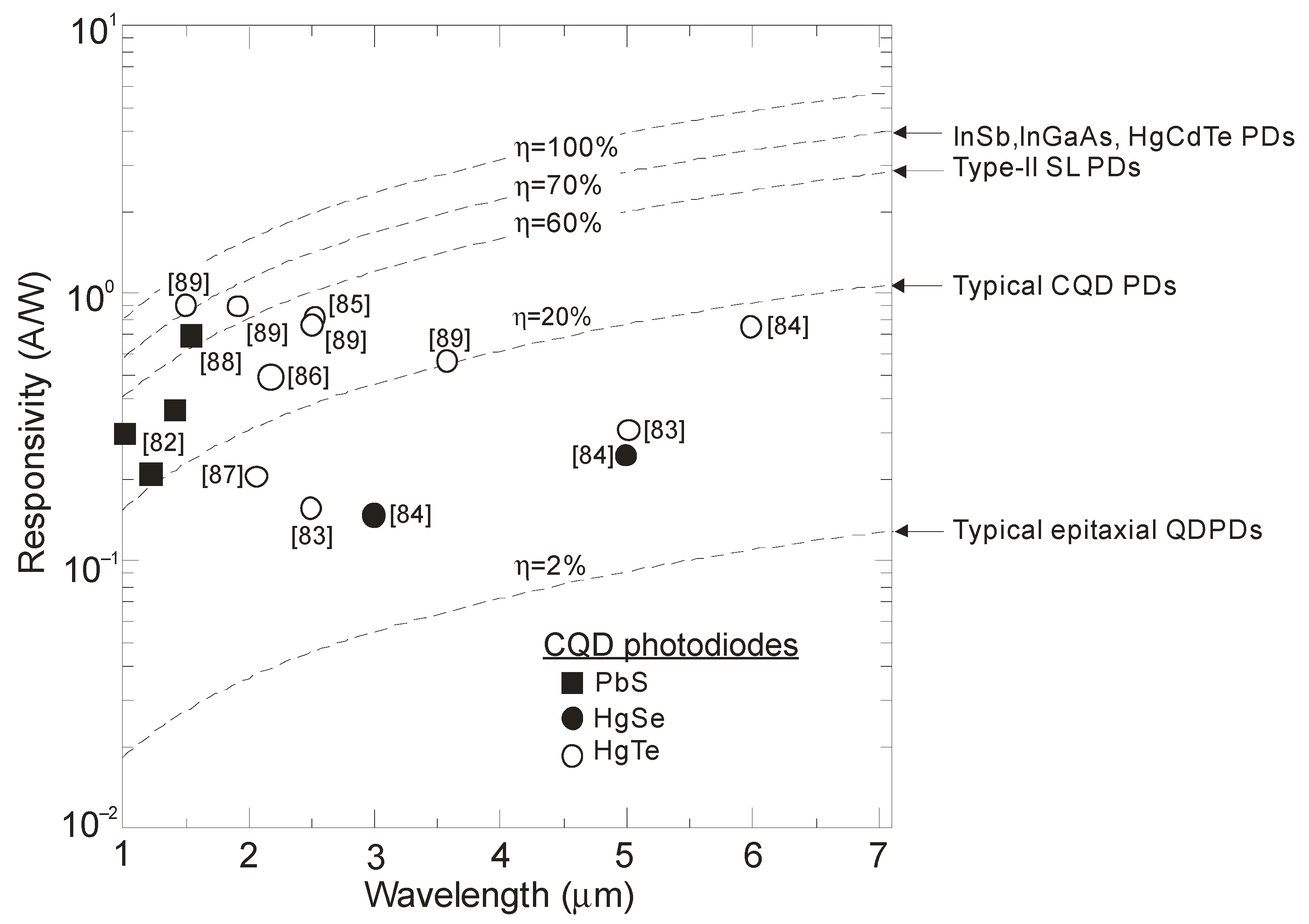
The CQD-based photodiodes’ current responsivity was reported within the range of 100 mA/W-1 A/W, which corresponds to external quantum efficiency ~10–80%, being higher in the short-wavelength infrared region (SWIR) (refer to Figure 16). These external quantum efficiencies (EQEs) are significantly higher than reached for epitaxial (self-organising) QD photodetectors—typically reported at ~2%. Typical QEs for commercially available InGaAs, InSb, HgCdTe and T2SL-based detectors are presented in Figure 16.
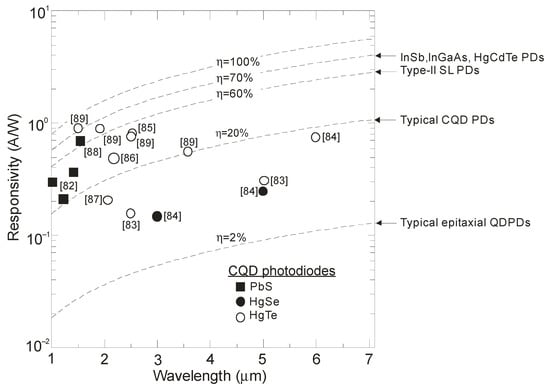
Figure 16.
Current responsivity versus wavelength for different IR technologies at 300 K. The experimental data are extracted from Refs. [82,83,84,85,86,87,88,89]. PDs—photodiodes.
The CQD layers are reported to be amorphous, allowing integration with ROIC substrates, as presented in Figure 17, with no pixel or array size limitations and a simple fabrication procedure. The CQD-based detectors’ monolithic integration into ROIC does not demand any hybridization process. The single pixels are defined by the ROIC’s metal pads. To synthesize colloidal nanocrystals, the compounds are injected into a flask and the required shape and size are reached by the reagent concentrations’ monitoring, ligand selection and temperature. This top-surface photodetector offers a 100% fill factor and is compatible with postprocessing CMOS electronics.
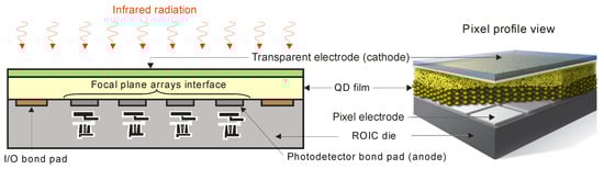
Figure 17.
The CQD-based monolithic IR array.
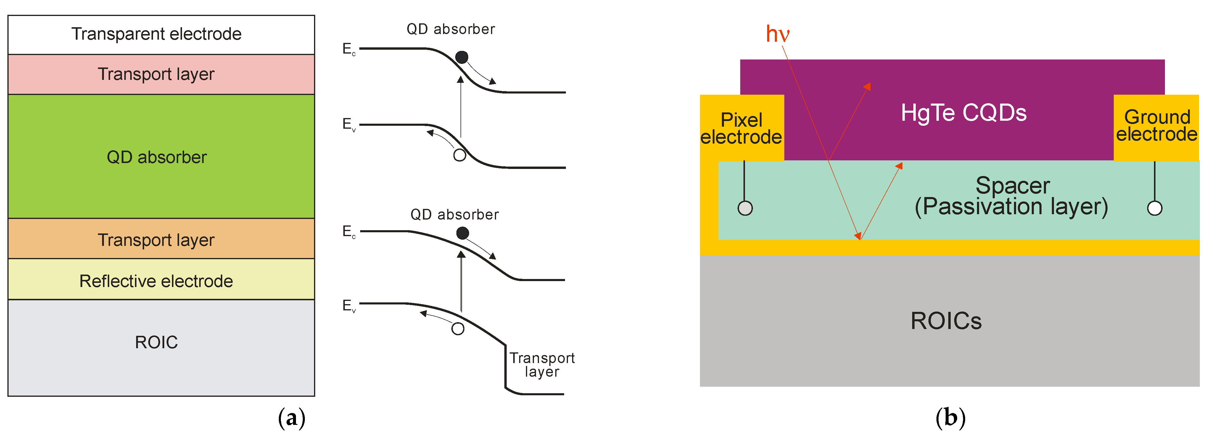
The most common photodiode stack accompanied by bandgap diagrams is presented in Figure 18a. The structure with a QD absorber contains additional thin-film transport layers made of metal oxides, organics (or 2D materials) monolithically integrated on CMOS read-out integrated circuits. The internal electric field directs electrons and holes in opposite directions through the transport layers. As shown, photodiode structures are fabricated in either homojunction form (top diagram) or heterojunction form (bottom diagram).
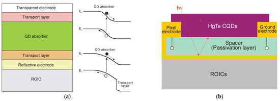
Figure 18.
Thin-film CQD photodiodes: (a) the most common photodiode stacks together with bandgap diagrams for homojunction and heterojunction; (b) the cross-section schematic of the resonant-cavity enhanced pixel of HgTe CQD imager (after Ref. [56]).
Increasing the thickness of the CQD layers, and at the same time an increase in the radiation absorption, is practically challenging due to the high likelihood of crack formation in the CQD film and the limited diffusion length of photoexcited carriers in CQD layers. A short diffusion length is a consequence of the low mobility of the carriers (several cm2/Vs in PbS QDs and below 1 cm2/Vs in HgTe QDs). Therefore, many recent efforts have focused on integrating CQD thin films with resonant optical structures to enhance light absorption. Photonic structures such as back reflectors, gold gratings and simplified Helmholtz resonators have been shown to confine and concentrate incident electromagnetic fields, thereby increasing the EQE of the CQD-based devices. Figure 18b presents an example of the pixel cross-section of a HgTe CQD FPA with the thickness of the absorption layer around 400 nm [56]. The pixel contains a pair of electrodes, the pixel electrode, which acts as both an electrical contact and as a back reflector and the ground electrode. The detector is biased by the pixel and ground electrodes.
In the fabrication of CQD photodetectors, the post-synthesis ligand exchange process is perhaps the most critical step in determining the detector’s ultimate performance. Ligands are molecules bound on the surface of a CQD. Due to the high surface-to-volume ratio, the surface has a strong influence on the CQD’s physical properties and surface ligands play an important role in the CQD’s stability and electrical properties. The aim of the ligand exchange process is to transfer the QDs to suitable ligands and solvents, control the majority carrier type and tune/increase the charge mobility. To reach efficient carrier transport, isolating long organic ligands should be replaced by small and/or ionic ligands. Efficient ligand exchange routes have been presented in the literature [31,88,89,90,91].
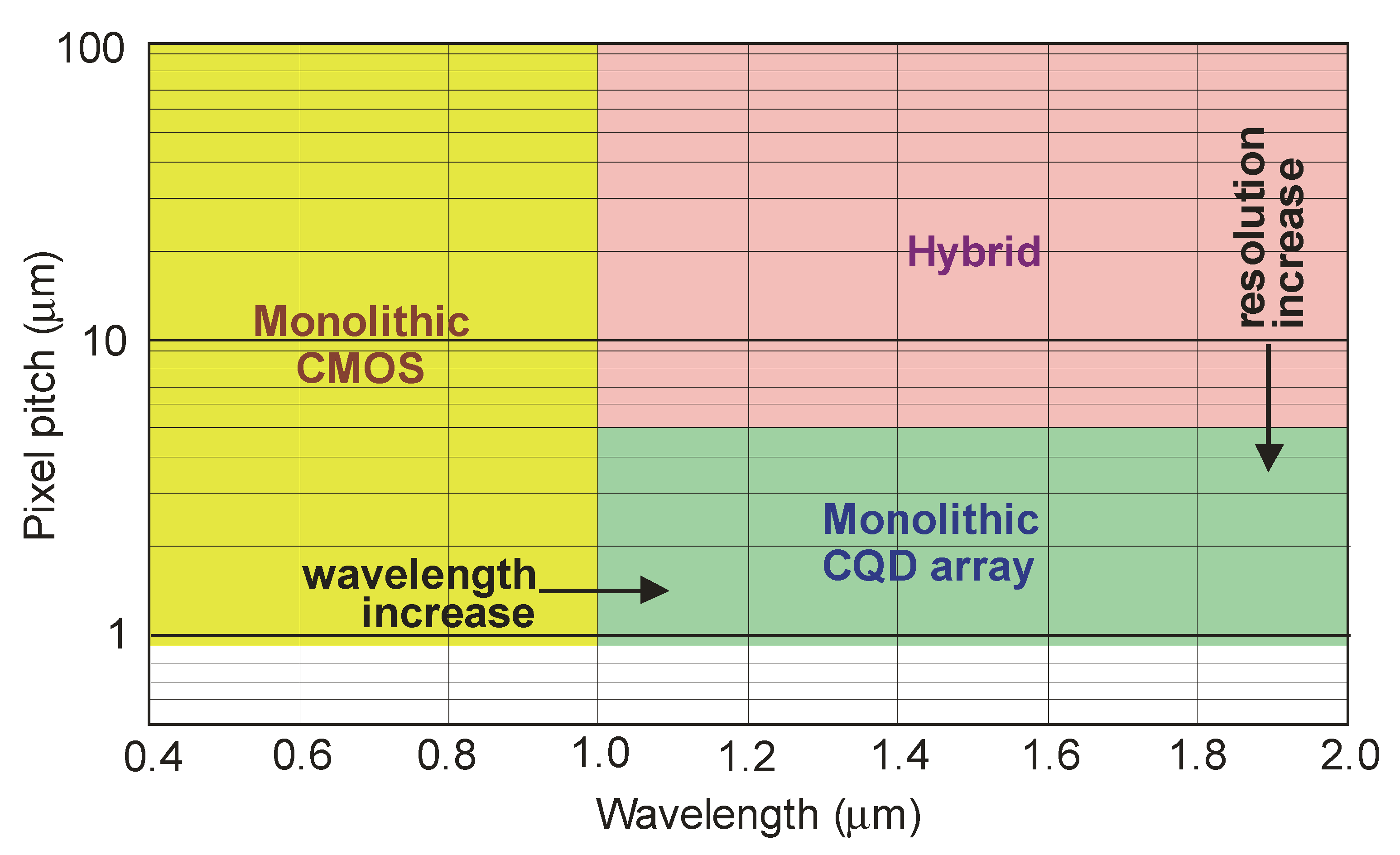
The lead chalcogenide family is mostly represented by lead sulfide (PbS) CQDs operating in the 1–3 μm NIR spectral range [92]. PbS CQD vertical technology, including the solution process, is compatible with the CMOS read-out technology used in monolithic FPA fabrication. The 100-nm-thick PbS CQD stacks may be implemented as effective active layers [93]. The conventional hybrid FPAs are normally restricted to 1 megapixel range arrays due to the small detector wafer and low throughput. In this configuration, a 5 μm pixel pitch was reported [3]. With a thin-film active layer integrated monolithically with ROIC, a <1 μm submicron pixel size can be fabricated (Figure 19). Currently, the CMOS VIS sensor state-of-the-art is 0.9 μm [3].
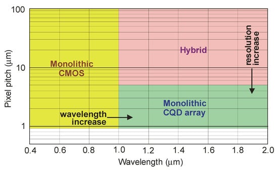
Figure 19.
Monolithic CQD array state-of-the-art—higher resolution than hybrid alternatives and longer wavelength than monolithic Si (after Ref. [93]).
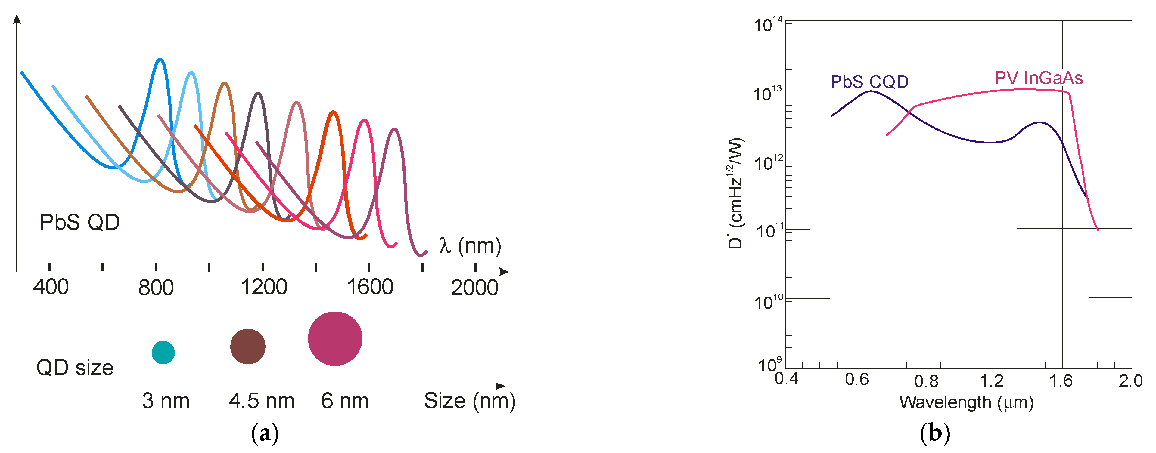
Figure 20a shows the absorption peak’s dependence on the nanocrystal size, where, for a 5.5 nm diameter, the peak absorption occurs at 1440 nm, and for 3.4 nm, the peak could be reached at 980 nm, respectively. This size-dependent flexibility can be implemented in hyperspectral sensors. The SWIR PbS CQD reached detectivities >1012 Jones (see Figure 20b) and QEs comparable to commercial 300 K InGaAs photodiodes. Vafaie et al. [88] reported on a high-concentration bromine processing and passivation step to enhance the responsivity of a 1550 nm PbS. The photodiode exhibited 80% EQE and a 10 ns response time, being the lowest reported fall time of an SWIR device fabricated by solution-processed materials.
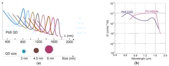
Figure 20.
PbS CQD detector: (a) spectral responsivity dependence on QD size (after Ref. [93]) and (b) detectivity for PbS CQD and InGaAs photodiodes (after Ref. [94]).
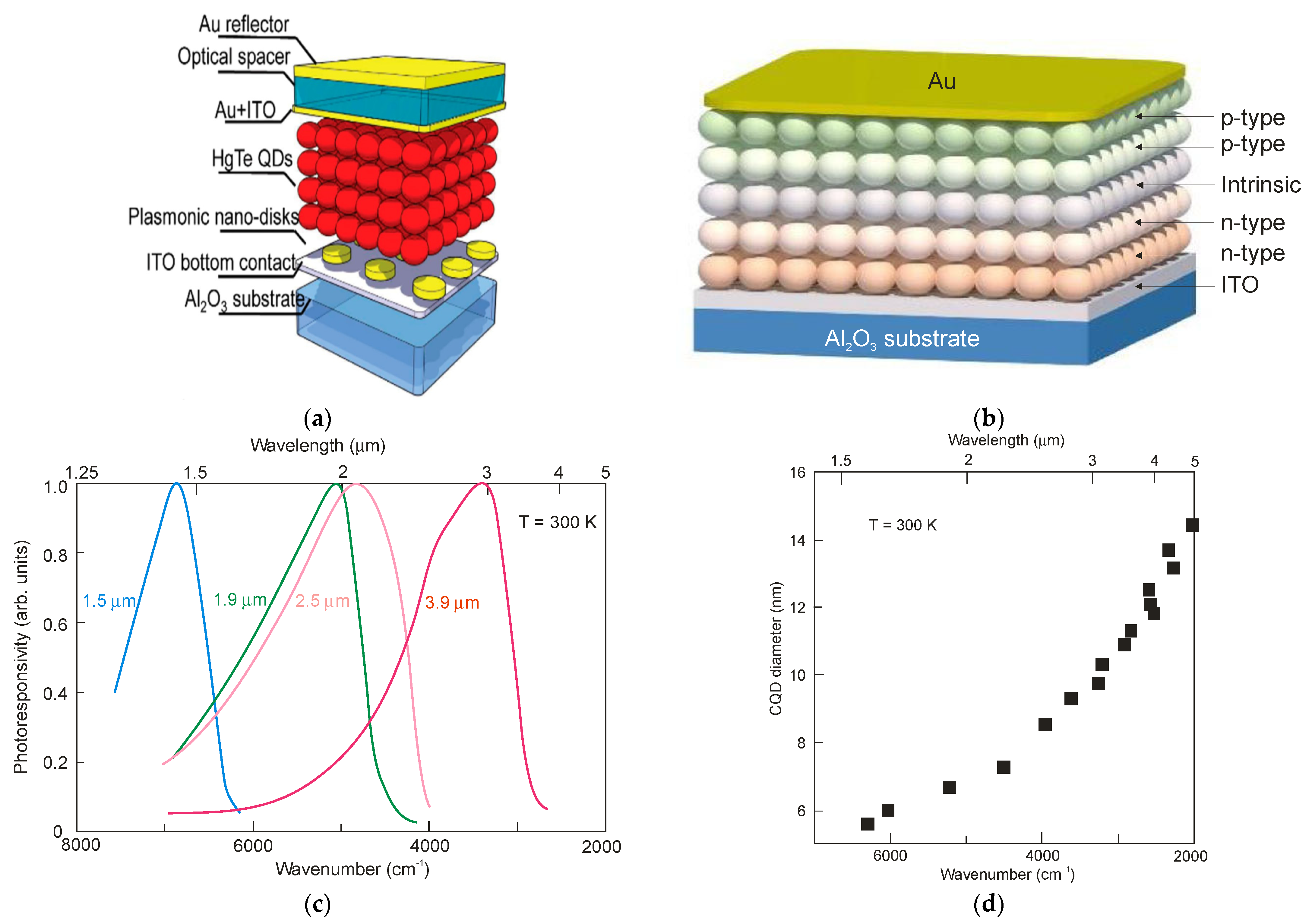
HgTe CQDs exhibit a spectral response within the SWIR-THz ranges. The first BLIP HgTe CQD photovoltaic detector operating in the MWIR (λc = 5.25 μm at 90 K) was demonstrated in 2015 by Guyot-Sionnest et al. [95]. The low carrier mobility in MWIR CQD films hinders the detector’s performance. This drawback could be circumvented by a proper CQD chemical treatment. Further progress in the sensitivity and time response was reached by Ag2Te heavily p-type doping [96]. Figure 21a shows the HgTe CQD photovoltaic detector design on an indium tin oxide (ITO)/sapphire substrate. The ~400 nm HgTe CQDs were deposited layer-by-layer by drop-casting. A solution of ~10 nm Ag2Te nanoparticles was then spun over the HgTe layer to create a strongly p-doped HgTe CQD top layer. A two/three times increase in D* was reached for the detector supported by a plasmonic nano-disc in comparison with a device without an absorption enhancement.

Figure 21.
HOT HgTe CQD photodiodes: (a) the structure with plasmonic discs [96]; (b) cross-section of homojunction p-i-n photodiode [31]; (c) CQD p-i-n HgTe homojunction photoresponse with λc equal to 1.5 μm, 1.9 μm, 2.5 μm and 3.6 μm [89]; (d) bandgap edge dependence on QD size [89].
More recently, gradient homojunction HgTe CQD photodiodes (see Figure 21b), using improved ligand exchange methods, have achieved even better rectification behavior via gradual doping level changes, leading to an increase in room-temperature detectivity to D* > 109 Jones for a cut-off wavelength close to 4 μm [31]. Figure 21c shows the 300 K photoresponse spectra of CQD p-i-n HgTe homojunctions with λc equal to 1.5 μm, 1.9 μm, 2.5 μm and 3.6 μm, being related to the absorption’s dependence on the QD size (see Figure 21d).
Figure 22 collects the highest published detectivities for selected photodetectors (PC-PbS, PC-PbSe, PV-Si, PV-InGaAs, PV-HgCdTe and CQD IR photodiodes) operating at 300 K. The presented data indicate sub-BLIP performance. The performance trend lines for HgCdTe photodiodes, IB QCIPs and 2D material photodetectors are also presented based on the experimental data collected in Figure 6. The detectivity of the CQD photodetectors in the MWIR region is comparable to that of HgCdTe photodiodes, indicating significant progress in CQD development. This progress is particularly evident in the SWIR, where the CQD-based detectors’ performance is even higher; however, the CQD photodiodes’ high detectivities in the SWIR and MWIR do not correlate with the high dark current densities marked in Figure 10. As presented in this figure, the current densities of CQD photodiodes are higher than those observed for SWIR HgCdTe photodiodes. These contradictory data are probably due to errors made in the measurements of the detector parameters, as pointed out in several papers [57,58,59,60].
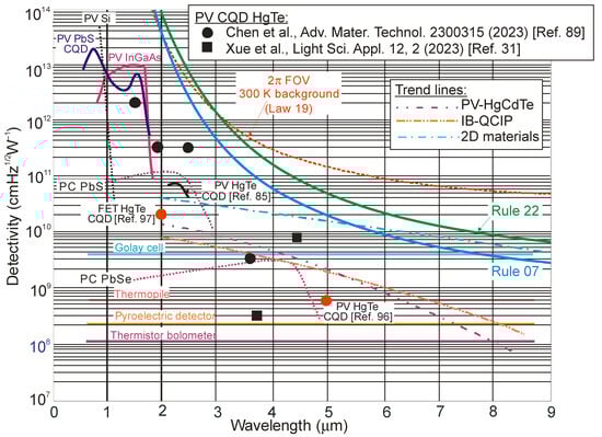
Figure 22.
Room-temperature detectivity for CQD photodiodes [31,85,89,96,97] and commercially available photodetectors (PV-Si and InGaAs, PC-PbS and PbSe, HgCdTe photodiodes (solid lines)). For comparison reasons, the trend lines for HgCdTe photodiodes, IB-QCIPs and 2D material photodetectors are also shown based on the data presented in Figure 6. PC—photoconductor, PV—photodiode.
The majority of the CQD detector research has been directed towards the single-pixel devices but CQDs offer also potential as an alternative in the traditional image sensor field, advancing from Si compatibility, solution processability and simplified device fabrication [94,97]. To date, several studies of SWIR and MWIR imagers have been reported. It is predicted to extend the spectral ranges to longer wavelengths. Table 3 summarizes key figures of merit for different monolithic CQD image sensors. This monolithic manufacturing provides affordability for many applications that could not consider IR data collection, such as smart agriculture, medical, surveillance and consumer applications and the automotive sector.
Table 3.
Figures of merit of CQD photovoltaic image sensors.
7. Conclusions
Currently, microbolometer arrays are the most widely used for uncooled IR detectors; however, these thermal detectors exhibit modern sensitivity and limited response times—usually in the millisecond range—and are not very useful for applications requiring multispectral detection. Bolometric detection typically cannot compete with the sensitivity or time response of semiconductor-based photon detectors. To circumvent this limitation, further efforts have been directed towards room-temperature photon detectors with better sensitivity and shorter response times.
Despite long-standing concerns regarding HgCdTe’s uniformity and toxicity [99], this compound occupies the main position among HOT photodetectors, especially in the LWIR range. For more than 60 years, HgCdTe has successfully competed with alternative technologies to include extrinsic silicon devices, lead–tin telluride devices, Schottky barriers on silicon, AlGaAs multiple quantum wells, T2SL and especially silicon microbolometers. Lately, important progress has been demonstrated in the fabrication of IR LDS detectors (2D materials and particularly CQDs) to include possible integration into imaging cameras. Both technologies have become exciting frontiers in the MWIR. It is expected that nano-fabrication and micro-electromechanical (MEMs) technology, as well as direct integration with CMOS architectures, will lead to improvements in and the widespread commercialization of FPAs containing pixels made of 2D materials and CQDs. However, given the current state of both technologies, several issues need to be addressed.
- The misinterpretation of layered photodetector performance due to incorrect noise calculations, the incorrect assessment of the device’s active area and radiation power density and the contradictory bandwidth of measured responsivity and noise.
- The current fabrication of 2D structures, which is mostly restricted to materials exfoliated from bulk crystals, with very limited yields, scalability and reproducibility. As a result, the nonuniformity in the spectral response and response times highly deteriorates FPAs’ performance.
- Further improved ligand exchange methods combined with enhanced photon collection are required to increase the CQD-based photodetectors’ performance.
- Although the performance of IB QCIPs is comparable to that of HgCdTe photodiodes, their complex structures with multiple interfaces and strained thin layers cause problems in technology development and drive up production costs.
HgCdTe BLIP’s ultimate HOT performance limit has not been reached. To reach this limit, a ~1013 cm−3 doping concentration in the active region is required, which was recently reported by Teledyne Technologies. It has been shown that this doping level in the active region allows one to reach BLIP performance for p-i-n HgCdTe photodiodes operating above 3 μm [12,50]. It will be difficult to approach the performance presented by HgCdTe photodiodes for 2D and CQD photodetectors. This statement is supported by an analysis of the ~α/Gth standard as a figure of merit for IR detectors. Teledyne has presented fully depleted 640 × 512 arrays (MWIR and LWIR operating at up to 250 and 160 K) [12,100], paving the way for the unique possibility of producing arrays with the largest format. In the next decade, HgCdTe photodiode arrays are expected to operate at 300 K in the MWIR and LWIR.
There are different methods of light coupling in a photodetector to enhance the quantum efficiency. In general, these absorption enhancement methods can be divided into four categories that use optical concentration, antireflection structures, an optical patch increase or light localization (e.g., using metasurface [101,102]). These methods can be used for photodetectors fabricated with different material systems. In our paper, we focused on the impact of the basic physical properties of different materials on the performance of photodetectors.
The future commercialization of next-generation HOT photodetectors (2D and CQD materials) will depend on their large-scale integration with existing photonic and electronic platforms, such as CMOS technologies; high operability; spatial uniformity; temporal stability; and affordability. Given this, success in the commercialization of CQD photodetectors appears to be feasible. However, there is no doubt that QD image sensors will penetrate more compact, less demanding markets and reach a high pixel density, while hybrid FPAs will retain the dominant position for high-end applications with stringent requirements.
Author Contributions
Conceptualization, A.R., W.H. and P.M.; methodology, M.K. and P.M.; software, M.K.; validation, A.R., W.H. and P.M.; formal analysis, M.K.; investigation, M.K. and P.M.; resources, M.K.; data curation, M.K.; writing—original draft preparation, A.R. and P.M.; writing—review and editing, P.M.; visualization, A.R. and M.K.; supervision, P.M.; project administration, A.R. and P.M.; funding acquisition, A.R. and P.M. All authors have read and agreed to the published version of the manuscript.
Funding
This research was funded by the National Science Center, Poland—grant nos. UMO-2019/33/B/ST7/00614, UMO-2021/41/B/ST7/01532; and the Science and Technology Commission of Shanghai Municipality—grant no. 23WZ2500400.
Institutional Review Board Statement
Not applicable.
Informed Consent Statement
Not applicable.
Data Availability Statement
All data generated or analyzed during this study are included in this published article.
Conflicts of Interest
The authors declare no conflict of interest.
References
- Piotrowski, J.; Rogalski, A. High-Operating-Temperature Infrared Photodetectors; SPIE Press: Bellingham, WA, USA, 2007. [Google Scholar]
- Piotrowski, J.; Rogalski, A. Comment on “Temperature limits on infrared detectivities of InAs/InxGa1–xSb superlattices and bulk Hg1–xCdxTe” [J. Appl. Phys. 1993, 74, 4774]. J. Appl. Phys. 1996, 80, 2542–2544. [Google Scholar] [CrossRef]
- Rogalski, A. Scaling infrared detectors—Status and outlook. Rep. Prog. Phys. 2022, 85, 126501. [Google Scholar]
- Chu, J.H.; Li, B.; Liu, K.; Tang, D. Empirical rule of intrinsic absorption spectroscopy in Hg1−xCdxTe. J. Appl. Phys. 1994, 75, 1234. [Google Scholar] [CrossRef]
- Vurgaftman, I.; Belenky, G.; Lin, Y.; Donetsky, D.; Shterengas, L.; Kipshidze, G.; Sarney, W.L.; Svensson, S.P. Interband absorption strength in long-wave infrared type-II superlattices with small and large superlattice periods compared to bulk materials. Appl. Phys. Lett. 2016, 108, 222101. [Google Scholar] [CrossRef]
- Klipstein, P.C.; Livneh, Y.; Glozman, A.; Grossman, S.; Klin, O.; Snapi, N.; Weiss, E. Modeling InAs/GaSb and InAs/InAsSb superlattice infrared detectors. J. Electron. Mater. 2014, 43, 2984. [Google Scholar] [CrossRef]
- Jariwala, D.; Davoyan, A.R.; Wong, J.; Atwater, H.A. Van der Waals materials for atomically-thin photovoltaics: Promise and outlook. ACS Photonics. 2017, 4, 2962–2970. [Google Scholar] [CrossRef]
- Rogalski, A. Van der Waals materials for HOT infrared detectors: A review. Opto-Electron. Rev. 2022, 30, el40551. [Google Scholar]
- Krishnamurthy, S.; Casselman, T.N. A detailed calculation of the Auger lifetime in p-type HgCdTe. J. Electron. Mater. 2000, 29, 828–831. [Google Scholar] [CrossRef]
- Kinch, M.A.; Aqariden, F.; Chandra, D.; Liao, P.-K.; Schaake, H.F.; Shih, H.D. Minority carrier lifetime in p-HgCdTe. J. Electron. Mater. 2005, 34, 880–884. [Google Scholar] [CrossRef]
- Kinch, M.A. State-of-the-Art Infrared Detector Technology; SPIE Press: Bellingham, WA, USA, 2014. [Google Scholar]
- Lee, D.; Dreiske, P.; Ellsworth, J.; Cottier, R.; Chen, A.; Tallaricao, S.; Yulius, A.; Carmody, M.; Piquetteb, E.; Zandian, M.; et al. Law 19—The ultimate photodiode performance metric. Proc. SPIE 2020, 11407, 114070X. [Google Scholar]
- Kopytko, M.; Rogalski, A. Performance evaluation of type-II superlattice devices relative to HgCdTe photodiodes. IEEE Trans. Electron. Devices 2022, 69, 2992–3002. [Google Scholar]
- Yang, J.; Xu, R.; Pei, J.; Myint, Y.W.; Wang, F.; Wang, Z.; Zhang, S.; Yu, Z.; Lu, Y. Optical tuning of exciton and trion emissions in monolayer phosphorene. Light: Sci. Appl. 2015, 4, e312. [Google Scholar]
- Vargas-Bernal, R. Graphene against Other Two-Dimensional Materials: A Comparative Study on the Basis of Photonic Applications; IntechOpen: London, UK, 2017. [Google Scholar] [CrossRef]
- Amani, M. Two-Dimensional Semiconductor Optoelectronics; Technical Report No. UCB/EECS-2021-16; University of California: Berkeley, CA, USA, 2021; Available online: http://www2.eecs.berkeley.edu/Pubs/TechRpts/2021/EECS-2021-16.pdf (accessed on 28 August 2023).
- Higgins, W.M.; Seiler, G.N.; Roy, R.G.; Lancaster, R.A. Standard relationships in the properties of Hg1–xCdxTe. J. Vac. Sci. Technol. 1989, A7, 271–275. [Google Scholar]
- Lawson, W.D.; Nielson, S.; Putley, E.H.; Young, A.S. Preparation and properties of HgTe and mixed crystals of HgTe-CdTe. J. Phys. Chem. Solids 1959, 9, 325–329. [Google Scholar]
- Tennant, W.E.; Lee, D.; Zandian, M.; Piquette, E.; Carmody, M. MBE HgCdTe technology: A very general solution to IR detection, descibrd by ‘Rule 07’, a very convenient heuristic. J. Electron. Mater. 2008, 37, 1406–1410. [Google Scholar]
- Zandian, M. Rule-22: An update to Rule-07. The 2022 U.S. Workshop on the Physics and Chemistry of II-VI Materials, 2022. J. Electron. Mater. 2023, in press. [Google Scholar]
- Gravrand, O.; Rothman, J.; Delacourt, B.; Boulard, F.; Lobre, C.; Ballet, O.H.; Santailler, J.L.; Cervera, C.; Brellier, D.; Pere-Laprene, N.; et al. Shockley–Read–Hall lifetime study and implication in HgCdTe photodiodes for IR detection. J. Electron. Mater. 2018, 47, 5680–5690. [Google Scholar]
- Hackiewicz, K.; Kopytko, M.; Gawron, W. MOCVD-grown HgCdTe photodiodes optimized for HOT conditions and a wide IR range. Sens. Actuator A Phys. 2020, 309, 112008. [Google Scholar]
- Wu, D.; Li, J.; Dehzangi, A.; Razeghi, M. Mid-wavelength infrared high operating temperature pBn photodetectors based on type-II InAs/InAsSb superlattice. AIP Adv. 2020, 10, 025018. [Google Scholar]
- Delli, E.; Letka, V.; Hodgson, P.D.; Repiso, E.; Hayton, J.P.; Craig, A.P.; Lu, Q.; Beanland, R.; Krier, A.; Marshall, A.R.J.; et al. Mid-infrared InAs/InAsSb superlattice nBn photodetector monolithically integrated onto silicon. ACS Photonics 2019, 6, 538–544. [Google Scholar]
- Pusz, W.; Kowalewski, A.; Martyniuk, P.; Gawron, W.; Plis, E.; Krishna, S.; Rogalski, A. Mid-wavelength infrared type-II InAs/GaSb superlattice interband cascade photodetectors. Opt. Eng. 2014, 53, 043107. [Google Scholar]
- Gawron, W.; Kubiszyn, Ł.; Michalczewski, K.; Manyk, T.; Piotrowski, J.; Martyniuk, P. The performance of the ICIP Ga-free superlattice longwave infrared photodetector for high operating temperature. Infrared Phys. Technol. 2023, 128, 104499. [Google Scholar]
- Amani, M.; Regan, E.; Bullock, J.; Ahn, G.H.; Javey, A. Mid-wave infrared photoconductors based on black phosphorus-arsenic alloys. ACS Nano 2017, 11, 11724–11731. [Google Scholar] [PubMed]
- Lukman, S.; Ding, L.; Xu, L.; Tao, Y.; Riis-Jensen, A.C.; Zhang, G.; Wu, Q.Y.S.; Yang, M.; Luo, S.; Hsu, C.; et al. High oscillator strength interlayer excitons in two-dimensional heterostructures for mid-infrared photodetection. Nat. Nanotechnol. 2020, 15, 675–682. [Google Scholar] [PubMed]
- Long, M.; Wang, Y.; Wang, P.; Zhou, X.; Xia, H.; Luo, C.; Huang, S.; Zhang, G.; Yan, H.; Fan, Z.; et al. Palladium diselenide long-wavelength infrared photodetector with high sensitivity and stability. ACS Nano 2019, 13, 2511–2519. [Google Scholar]
- Zeng, L.; Wu, D.; Jie, J.; Ren, X.; Hu, X.; Lau, S.; Chai, Y.; Tsang, Y.H. Van der Waals epitaxial growth of mosaic-like 2D platinum ditelluride layers for room-temperature mod-infrared photodetection up to 10.6 µm. Adv. Mater. 2020, 32, 2004412. [Google Scholar]
- Xue, X.; Chen, M.; Luo, Y.; Qin, T.; Tang, X.; Hao, Q. High-operating-temperature mid-infrared photodetectors via quantum dot gradient homojunction. Light Sci. Appl. 2023, 12, 2. [Google Scholar]
- Long, M.; Gao, A.; Wang, P.; Xia, H.; Ott, C.; Pan, C.; Fu, Y.; Liu, E.; Chen, X.; Lu, W.; et al. Room temperature high-detectivity mid-infrared photodetectors based on black arsenic phosphorus. Sci. Adv. 2017, 3, e1700589. [Google Scholar]
- Du, S.; Lu, W.; Ali, A.; Zhao, P.; Shehzad, K.; Guo, H.; Ma, L.; Liu, X.; Pi, X.; Wang, P.; et al. A broadband fluorographene photodetector. Adv. Mater. 2017, 29, 1700463. [Google Scholar]
- Chen, Y.; Wang, Y.; Wang, Z.; Gu, Y.; Ye, Y.; Chai, X.; Ye, J.; Chen, Y.; Xie, R.; Zhou, Y.; et al. Unipolar barrier photodetectors based on van der Waals heterostructures. Nat. Electron. 2021, 4, 357–363. [Google Scholar]
- Ni, Z.; Ma, L.; Du, S.; Xu, Y.; Yuan, M.; Fang, H.; Wang, Z.; Xu, M.; Li, D.; Yang, J.; et al. Plasmonic silicon quantum dots enabled high-sensitivity ultrabroadband photodetection of graphene-based hybrid phototransistors. ACS Nano 2017, 11, 9854–9862. [Google Scholar] [CrossRef] [PubMed]
- Wang, S.; Liu, H.; Cao, Z.; Wang, X.; Zhang, L.; Ding, J.; Xue, Y.; Han, T.; Li, F.; Shan, L.; et al. Highly sensitive long-wave infrared photodetector based on two-dimensional hematite α-Fe2O3. Adv. Optical Mater. 2023, 2300382. [Google Scholar] [CrossRef]
- Tian, P.; Wu, H.; Tang, L.; Xiang, J.; Ji, R.; Lau, S.P.; Te, K.S.; Guo, W.; Yao, Y.; Lig, L.-J. Ultrasensitive broadband photodetectors based on two-dimensional Bi2O2Te films. J. Mater. Chem. 2021, C9, 13713–13721. [Google Scholar] [CrossRef]
- Ye, L.; Wang, P.; Luo, W.; Gong, F.; Liao, L.; Liu, T.; Tong, L.; Zang, J.; Xu, J.; Hu, W. Highly polarization sensitive infrared photodetector based on black phosphorus-on-WSe2 photogate vertical heterostructure. Nano Energy 2017, 37, 53–60. [Google Scholar] [CrossRef]
- Lukman, S.; Ding, L.; Xu, L.; Tao, Y.; Riis-Jensen, A.C.; Zhang, G.; Wu, Q.Y.S.; Yang, M.; Luo, S.; Hsu, C.; et al. Reply to: Detectivities of WS2/HfS2 heterojunctions. Nat. Nano. 2022, 17, 220–221. [Google Scholar] [CrossRef]
- Available online: https://vigo.com.pl/wp-content/uploads/2017/06/VIGO-Catalogue.pdf (accessed on 28 August 2023).
- HOT MCT Detectors. Available online: http://www.teledynejudson.com/ (accessed on 28 August 2023).
- Rogalski, A.; Kopytko, M.; Martyniuk, P.; Hu, W. Trends in performance limits of the HOT infrared photodetectors. Appl. Sci. 2021, 11, 501. [Google Scholar] [CrossRef]
- Yu, X.; Yu, P.; Wu, D.; Singh, B.; Zeng, Q.; Lin, H.; Zhou, W.; Lin, J.; Suenaga, K.; Liu, Z.; et al. Atomically thin noble metal dichalcogenide: A broadband mid-infrared semiconductor. Nature Commun. 2018, 9, 1545. [Google Scholar] [CrossRef]
- Konstantatos, G. Current status and technological prospect of photodetectors based on two-dimensional materials. Nature Commun. 2018, 9, 5266. [Google Scholar] [CrossRef]
- Konstantatos, G.; Sargent, E.H. Solution-processed quantum dot photodetectors. Proc. IEEE 2009, 97, 1666–1683. [Google Scholar] [CrossRef]
- Konstantatos, G.; Badioli, M.; Gaudreau, L.; Osmond, J.; Bernechea, M.; Garcia de Arquer, F.P.; Gatti, F.; Koppens, F.H.L. Hybrid graphene-quantum dot phototransistors with ultrahigh gain. Nat. Nanotechnol. 2012, 7, 363–368. [Google Scholar] [CrossRef]
- Martyniuk, P.; Rogalski, A.; Krishna, S. Interband quantum cascade infrared photodetectors: Current status and future trends. Phys. Rev. Appl. 2022, 17, 027001. [Google Scholar] [CrossRef]
- Huang, W.; Rassela, S.M.S.; Li, L.; Massengale, J.A.; Yang, R.Q.; Mishima, T.D.; Santos, M.B. A unified figure of merit for interband and intersubband cascade devices. Infrared Phys. Technol. 2019, 96, 298. [Google Scholar] [CrossRef]
- Tian, Z.-B.; Godoy, S.E.; Kim, H.S.; Schuler-Sandy, T.; Montoya, J.A.; Krishna, S. High operating temperature interband cascade focal plane arrays. Appl. Phys. Lett. 2014, 105, 051109. [Google Scholar] [CrossRef]
- Lee, D.; Dreiske, P.; Ellsworth, J.; Cottier, R.; Chen, A.; Tallarico, S.; Yulius, A.; Carmody, M.; Piquette, E.; Zandian, M.; et al. Law 19—The ultimate photodiode performance metric. In Proceedings of the Extended Abstracts, The 2019 U.S. Workshop on the Physics and Chemistry of II-VI Materials, Chicago, IL, USA, 18–21 November 2019; pp. 13–15. [Google Scholar]
- Rhiger, D.R. Performance comparison of long-wavelength infrared type II superlattice devices with HgCdTe. J. Elect. Mater. 2011, 40, 1815–1822. [Google Scholar] [CrossRef]
- Klipstein, P.C.; Avnon, E.; Azulai, D.; Benny, Y.; Fraenkel, R.; Glozman, A.; Hojman, E.; Klin, O.; Krasovitsky, L.; Langof, L.; et al. Type II superlattice technology for LWIR detectors. Proc. SPIE 2016, 9819, 98190T. [Google Scholar]
- Rogalski, A. Infrared Detectors, 2nd ed.; CRC Press: Boca Raton, FL, USA, 2019. [Google Scholar]
- Steckel, J.S.; Josse, E.; Pattantyus-Abraham, A.G.; Bidaud, M.; Mortini, B.; Bilgen, H.; Arnaud, O.; Allegret-Maret, S.; Saguin, F.; Mazet, L.; et al. 1.62 μm global shutter quantum dot image sensor optimized for near and shortwave infrared. In Proceedings of the 2021 IEEE International Electron Devices Meeting (IEDM), San Francisco, CA, USA, 11–16 December 2021; pp. 23–24. [Google Scholar]
- Pejovic, V.; Lee, J.; Georgitzikis, E.; Li, Y.; Kim, J.H.; Lieberman, I.; Malinowski, P.E.; Heremans, P.D. CheynsThin-film photodetector optimization for high-performance short-wavelength infrared imaging. IEEE Electron. Device Lett. 2021, 42, 1196–1199. [Google Scholar] [CrossRef]
- Luo, Y.; Tan, Y.; Bi, C.; Zhang, S.; Xue, X.; Chen, M.; Hao, Q.; Liu, Y.; Tang, X. Megapixel large-format colloidal quantum-dot infrared imagers with resonant-cavity enhanced photoresponse. APL Photonics 2023, 8, 056109. [Google Scholar] [CrossRef]
- Bianconi, S.; Lauhon, L.J.; Mohseni, H. Exaggerated sensitivity in photodetectors with internal gain. Nat. Photonics 2012, 15, 714. [Google Scholar] [CrossRef]
- Rogalski, A. Detectivities of WS2/HfS2 heterojunctions. Nat. Nanotechnol. 2022, 17, 217–219. [Google Scholar] [CrossRef]
- Rogalski, A. Overestimating the performance of photon ultraviolet detectors. IEEE Electron. Device Lett. 2023, 44, 805–808. [Google Scholar] [CrossRef]
- Wang, F.; Zhang, T.; Xie, R.; Wang, Z.; Hu, W. How to characterize figures of merit two-dimensional photodetectors. Nat. Commun. 2023, 14, 2224. [Google Scholar] [CrossRef] [PubMed]
- Long, M.; Wang, P.; Fang, H.; Hy, W. Progress, challenges, and opportunities for 2D material based photodetectors. Adv. Funct. Mater. 2018, 29, 18003807. [Google Scholar] [CrossRef]
- Fang, H.; Hu, W. Photogating in low dimensional photodetectors. Adv. Sci. 2017, 4, 170323. [Google Scholar] [CrossRef] [PubMed]
- Zhang, Y.; Hellebusch, D.J.; Bronstein, N.D.; Ko Ogletree, C.D.F.; Salmeron, M.; Alivisatos, A.P. Ultrasensitive photodetectors exploiting electrostatic trapping and percolation transport. Nat. Commun. 2016, 7, 11924. [Google Scholar] [CrossRef]
- Luo, P.; Zhuge, F.; Wang, F.; Lian, L.; Liu, K.; Zhang, J.; Zhai, T. PbSe quantum dots sensitized high-mobility Bi2O2Se nanosheets for high-performance and broadband photodetection beyond 2 μm. ACS Nano 2019, 13, 9028–9037. [Google Scholar] [CrossRef] [PubMed]
- Kim, J.; Park, S.; Jang, H.; Koirala, N.; Lee, J.-B.; Kim, U.J.; Lee, H.-S.; Roh, Y.-G.; Lee, H.; Sim, S.; et al. Highly sensitive, gate-tunable, room-temperature mid-infrared photodetection based on graphene-Bi2Se3 heterostructure. ACS Photonics 2017, 4, 482–488. [Google Scholar] [CrossRef]
- Huo, N.; Gupta, S.; Konstantatos, G. MoS2-HgTe quantum dot hybrid photodetectors beyond 2 μm. Adv. Mater. 2017, 29, 1606576. [Google Scholar] [CrossRef]
- Yu, X.; Li, Y.; Hu, X.; Zhang, D.; Tao, Y.; Liu, Z.; He, Y.; Haque, M.A.; Liu, Z.; Wu, T.; et al. Narrow bandgap oxide nanoparticles coupled with graphene for high performance mid-infrared photodetection. Nat. Commun. 2018, 9, 4299. [Google Scholar] [CrossRef]
- Kwak, D.H.; Lim, D.H.; Ra, H.S.; Ramasamy, P.; Lee, J.S. High performance hybrid graphene-CsPbBr3-xIx perovskite nano-crystal photodetector. RSC Adv. 2016, 6, 65252–65256. [Google Scholar] [CrossRef]
- Rogalski, A. Infrared and Terahertz Detectors, 3rd ed.; CRC Press: Boca Raton, FL, USA, 2019. [Google Scholar]
- Kufer, D.; Nikitskiy, I.; Lasanta, T.; Navickaite, G.; Koppens, F.H.L.; Konstantatos, G. Hybrid 2D–0D MoS2–PbS quantum dot photodetectors. Adv. Mater. 2015, 27, 176. [Google Scholar] [CrossRef]
- Mudd, G.W.; Svatek, S.A.; Hague, L.; Makarovsky, O.; Kudrynskyi, Z.R.; Mellor, C.J.; Beton, P.H.; Eaves, L.; Novoselov, K.S.; Kovalyuk, Z.D.; et al. Broad-band photoresponsivity of mechanically formed InSe–Graphene van der Waals heterostructures. Adv. Mater. 2015, 27, 3760. [Google Scholar] [CrossRef] [PubMed]
- Wang, Z.; Wang, P.; Wang, F.; Ye, J.; He, T.; Wu, F.; Peng, M.; Wu, P.; Chen, Y.; Zhong, F.; et al. A noble metal dichalcogenide for high-performance field-effect transistors and broadband photodetectors. Adv. Funct. Mater. 2020, 30, 1907945. [Google Scholar] [CrossRef]
- Tong, L.; Huang, X.; Wang, P.; Ye, L.; Peng, M.; An, L.; Sun, Q.; Zhang, Y.; Yang, G.; Li, Z.; et al. Stable mid-infrared polarization imaging based on quasi-2D tellurium at room temperature. Nat. Commun. 2020, 11, 2308. [Google Scholar] [CrossRef] [PubMed]
- Huang, L.; Dong, B.; Guo, X.; Chang, Y.; Chen, N.; Huang, X.; Liao, W.; Zhu, C.; Wang, H.; Lee, C.; et al. Waveguide-integrated black phosphorus photodetector for mid-infrared applications. ACS Nano 2019, 13, 913. [Google Scholar] [CrossRef]
- Zhao, M.; Xia, W.; Wang, Y.; Luo, M.; Tian, Z.; Guo, Y.; Hu, W.; Xue, J. Nb2SiTe4: A stable narrow-gap two-dimensional material with ambipolar transport and mid-infrared response. ACS Nano 2019, 13, 10705. [Google Scholar] [CrossRef]
- Wu, D.; Guo, J.; Du, J.; Xia, C.; Zeng, L.; Tian, Y.; Shi, Z.; Tian, Y.; Li, X.J.; Tsang, Y.H.; et al. Highly polarization-sensitive, broadband, self-powered photodetector based on Graphene/PdSe2/Germanium heterojunction. ACS Nano 2019, 13, 9907. [Google Scholar] [CrossRef]
- Bullock, J.; Amani, M.; Cho, J.; Chen, Y.-Z.; Ahn, G.H.; Adinolfi, V.; Shrestha, V.R.; Gao, Y.; Crozier, K.B.; Chueh, Y.-L.; et al. Polarization-resolved black phosphorus/molybdenum disulfide mid-wave infrared photodiodes with high detectivity at room temperature. Nat. Photonics 2018, 12, 601. [Google Scholar] [CrossRef]
- Lai, J.; Liu, Y.; Ma, J.; Zhuo, X.; Peng, Y.; Lu, W.; Liu, Z.; Chen, J.; Sun, D. Broadband anisotropic photoresponse of the “Hydrogen Atom” version Type-II Weyl semimetal candidate TaIrTe4. ACS Nano 2018, 12, 4055. [Google Scholar] [CrossRef]
- Lai, J.; Liu, X.; Ma, J.; Wang, Q.; Zhang, K.; Ren, X.; Liu, Y.; Gu, Q.; Zhuo, X.; Lu, W.; et al. Anisotropic broadband photoresponse of layered type-II Weyl semimetal MoTe2. Adv. Mater. 2018, 30, 1707152. [Google Scholar] [CrossRef]
- Ahn, S.; Chung, H.; Chen, W.; Moreno-Gonzalez, M.A.; Vazquez-Mena, O. Optoelectronic response of hybrid PbS-QD/graphene photodetectors. J. Chem. Phys. 2019, 151, 234705. [Google Scholar] [CrossRef]
- Phillips, J. Evaluation of the fundamental properties of quantum dot infrared detectors. J. Appl. Phys. 2002, 91, 4590–4594. [Google Scholar] [CrossRef]
- Konstantatos, G.; Howard, I.; Fischer, A.; Hoogland, S.; Clifford, J.; Klem, E.; Levina, L.; Sargent, E.H. Ultrasensitive solution-cast quantum dot photodetectors. Nature 2006, 442, 180–183. [Google Scholar] [CrossRef] [PubMed]
- Tang, X.; Ackerman, M.M.; Chen, M.; Guyot-Sionnest, P. Dual-band infrared imaging using stacked colloidal quantum dot photodiodes. Nat. Photonics 2019, 13, 277–282. [Google Scholar] [CrossRef]
- Lhuillier, E. Optoelectronics of Confined Semiconductors: The Case of Colloidal Nanocrystals and Their Application to Photodetection. Available online: https://arxiv.org/ftp/arxiv/papers/1706/1706.02837.pdf (accessed on 28 August 2023).
- Ackerman, M.M.; Chen, M.; Guyot-Sionnest, P. HgTe colloidal quantum dot photodiodes for extended short-wave infrared detection. Appl. Phys. Lett. 2020, 116, 083502. [Google Scholar] [CrossRef]
- Tang, X.; Ackerman, M.M.; Shen, G.; Guyot-Sionnest, P. Towards infrared electronic eyes: Flexible colloidal quantum dot photovoltaic detectors enhanced by resonant cavity. Small 2019, 15, 1804920. [Google Scholar] [CrossRef]
- Tang, X.; Ackerman, M.M.; Guyot-Sionnest, P. Acquisition of hyperspectral data with colloidal quantum dots. Laser Photonics Rev. 2019, 13, 1900165. [Google Scholar] [CrossRef]
- Vafaie, M.; Fan, J.Z.; Najarian, A.M.; Ouellette, O.; Sagar, L.K.; Bertens, K.; Sun, B.; Garcia de Arquer, F.P.; Sargent, E.H. Colloidal quantum dot photodetectors with 10-ns response time and 80% quantum efficiency at 1550 nm. Matter 2021, 4, 1042–1053. [Google Scholar] [CrossRef]
- Chen, M.; Xue, X.; Qin, T.; Wen, C.; Hao, Q.; Tang, X. Universal homojunction design for colloidal quantum dot infrared photodetectors. Adv. Mater. Technol. 2023, 8, 2300315. [Google Scholar] [CrossRef]
- Wu, H.; Ning, Z. Tutorial: Lead sulphide colloidal quantum dot infrared photodetector. J. Appl. Phys. 2023, 133, 041101. [Google Scholar] [CrossRef]
- Song, H.; Tischenko, Y.; Wasserman, D.; Jeong, K.S. Quantum dot materials for mid-IR photodetection: Opinion. Opt. Mater. Express 2023, 15, 1328–1334. [Google Scholar] [CrossRef]
- Pejovic, V.; Georgitzikis, E.; Lee, J.; Lieberman, I.; Cheyns, D.; Heremans, P.; Malinowski, P.E. Infrared colloidal quantum dot image sensors. IEEE Trans. Electron. Devices 2022, 69, 2840–2850. [Google Scholar] [CrossRef]
- Malinowski, P.E.; Georgitzikis, E.; Maes, J.; Vamvaka, I.; Frazzica, F.; Van Olmen, J.; De Moor, P.; Heremans, P.; Hens, Z.; Cheyns, D. Thin-film quantum dot photodiode for monolithic infrared image sensors. Sensors 2017, 17, 2867. [Google Scholar] [CrossRef] [PubMed]
- Klem, E.J.D.; Gregory Temple, D.; Lewis, J. PbS colloidal quantum dot photodiodes for low-cost SWIR sensing. Proc. SPIE 2015, 9451, 945104. [Google Scholar]
- Guyot-Sionnest, P.; Roberts, J.A. Background limited mid-infrared photodetection with photovoltaic HgTe colloidal quantum dots. Appl. Phys. Lett. 2015, 107, 091115. [Google Scholar] [CrossRef]
- Tang, X.; Ackerman, M.M.; Guyot-Sionnest, P. Thermal imaging with plasmon resonance enhanced HgTe colloidal quantum dot photovoltaic devices. ACS Nano 2018, 12, 7362–7370. [Google Scholar] [CrossRef]
- Chen, M.; Lu, H.; Abdelazim, N.M.; Zhu, Y.; Wang, Z.; Ren, W.; Kershaw, S.V.; Rogach, A.L.; Zhao, N. Mercury telluride quantum dot based phototransistor enabling high-sensitivity room-temperature photodetection at 2000 nm. ACS Nano 2017, 11, 5614–5622. [Google Scholar] [CrossRef]
- SWIR Vision Systems. Acuros CQD 1920/1920L GigE SWIR Camera. Available online: https://www.swirvisionsystems.com/wp-content/uploads/Acuros-CQD-1920L-GigE-SWIR-Camera_003.pdf (accessed on 28 August 2023).
- Han, A.; Han, E.; Han Hv, E. Directive 2011/65/EU of The European Parliament and of the Council of 8 June 2011 on the restriction of the use of certain hazardous substances in electrical and electronic equipment. Off. J. Eur. Union 2011, L 174, 88–110. [Google Scholar]
- Jerram, P.; Beletic, J. Teledyne’s high performance infrared detectors for space missions. Proc. SPIE 2018, 11180, 111803D-2. [Google Scholar]
- Đorđevic, N.; Schwanninger, R.; Yarema, M.; Koepfli, S.; Yarema, O.; Salamin, Y.; Lassaline, N.; Cheng, B.; Yazdani, N.; Dorodnyy, A.; et al. Metasurface colloidal quantum dot photodetectors. ACS Photonics 2022, 9, 482–492. [Google Scholar] [CrossRef]
- Chen, Z.; Weng, Y.; Liu, J.; Guo, N.; Yu, Y.; Xiao, L. Dual-band perfect absorber for a mid-infrared photodetector based on a dielectric metal metasurface. Photonics Res. 2021, 9, 27–33. [Google Scholar] [CrossRef]


Disclaimer/Publisher’s Note: The statements, opinions and data contained in all publications are solely those of the individual author(s) and contributor(s) and not of MDPI and/or the editor(s). MDPI and/or the editor(s) disclaim responsibility for any injury to people or property resulting from any ideas, methods, instructions or products referred to in the content. |
© 2023 by the authors. Licensee MDPI, Basel, Switzerland. This article is an open access article distributed under the terms and conditions of the Creative Commons Attribution (CC BY) license (https://creativecommons.org/licenses/by/4.0/).