Appendix A
4H-SiC 2
m-CMOS technology has been developed by Fraunhofer IISB (Germany), and the main physical parameters and the electrical parameters evaluated at room temperature are reported in
Table A1.
Table A1.
Physical and electrical parameters of the 4H-SiC CMOS technology at r.t.
Table A1.
Physical and electrical parameters of the 4H-SiC CMOS technology at r.t.
| Parameter | Unit | Value |
|---|
| [nm] | 55 |
| [fFcm] | 345.31 |
| [fFcm] | 855.30 |
| [nFcm] | 62.78 |
| [V] | 5.8 |
| [V] | −8 |
| [cmVs] | 17.14 |
| [cmVs] | 3.52 |
The experimental transcharacteristics of
Figure A1 and the output characteristics of
Figure A2 are for PMOSFET and NMOSFET, with a form factor of 100
m/10
m and 10
m/10
m, respectively.
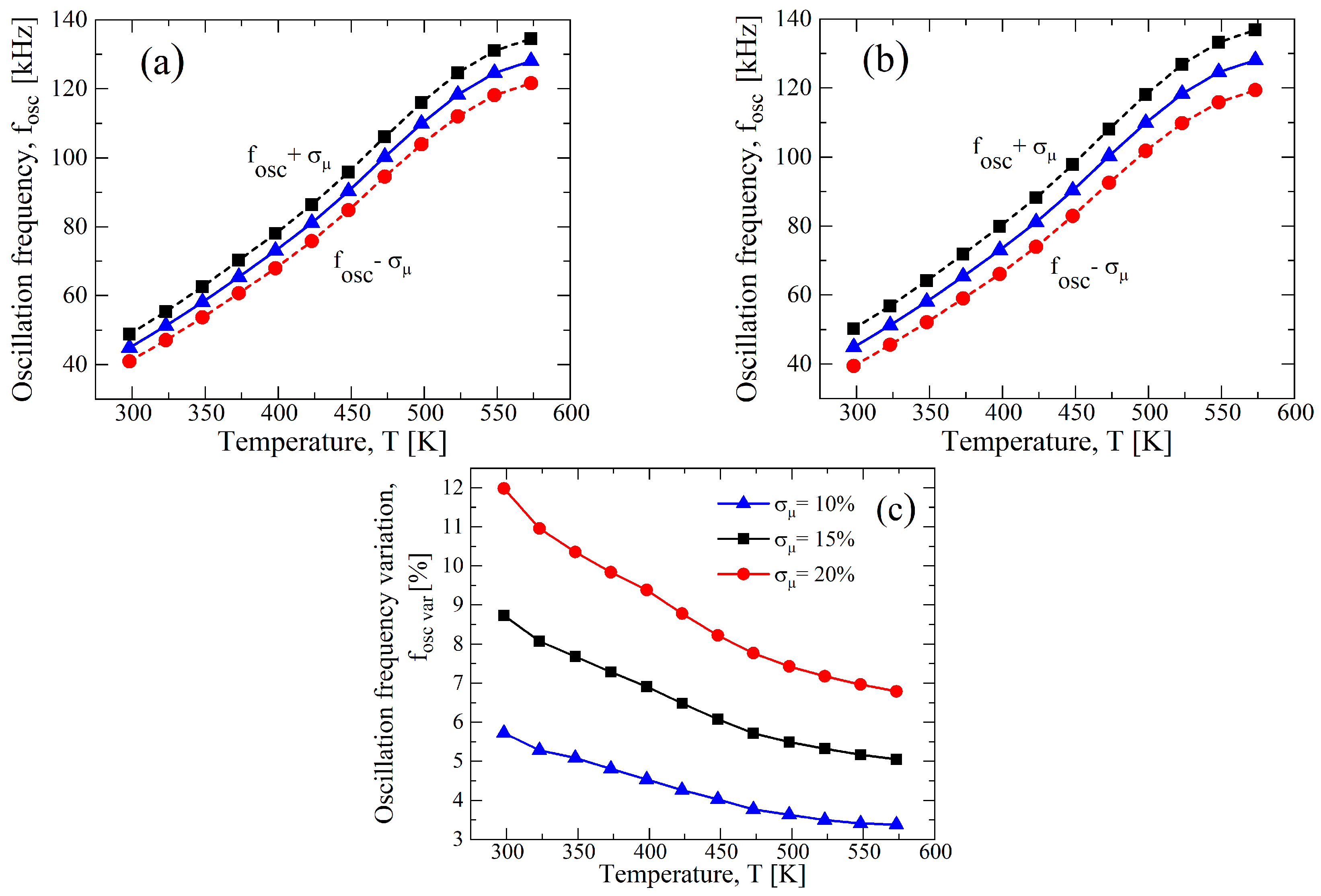
Figure A1.
Comparison between the experimental and Verilog-A numerical model transcharacteristics of lateral 4H-SiC. (a) PMOSFET with m/10 m and (b) NMOSFET with m/10 m. All the curves are at r.t., from 0.1 V to 20 V, and V.
Figure A1.
Comparison between the experimental and Verilog-A numerical model transcharacteristics of lateral 4H-SiC. (a) PMOSFET with m/10 m and (b) NMOSFET with m/10 m. All the curves are at r.t., from 0.1 V to 20 V, and V.
Figure A2.
Comparison between experimental and Verilog-A numerical model output characteristics of lateral 4H-SiC. (a) PMOSFET with m/10 m and (b) NMOSFET with m/10 m. All the curves are at r.t. and V.
Figure A2.
Comparison between experimental and Verilog-A numerical model output characteristics of lateral 4H-SiC. (a) PMOSFET with m/10 m and (b) NMOSFET with m/10 m. All the curves are at r.t. and V.
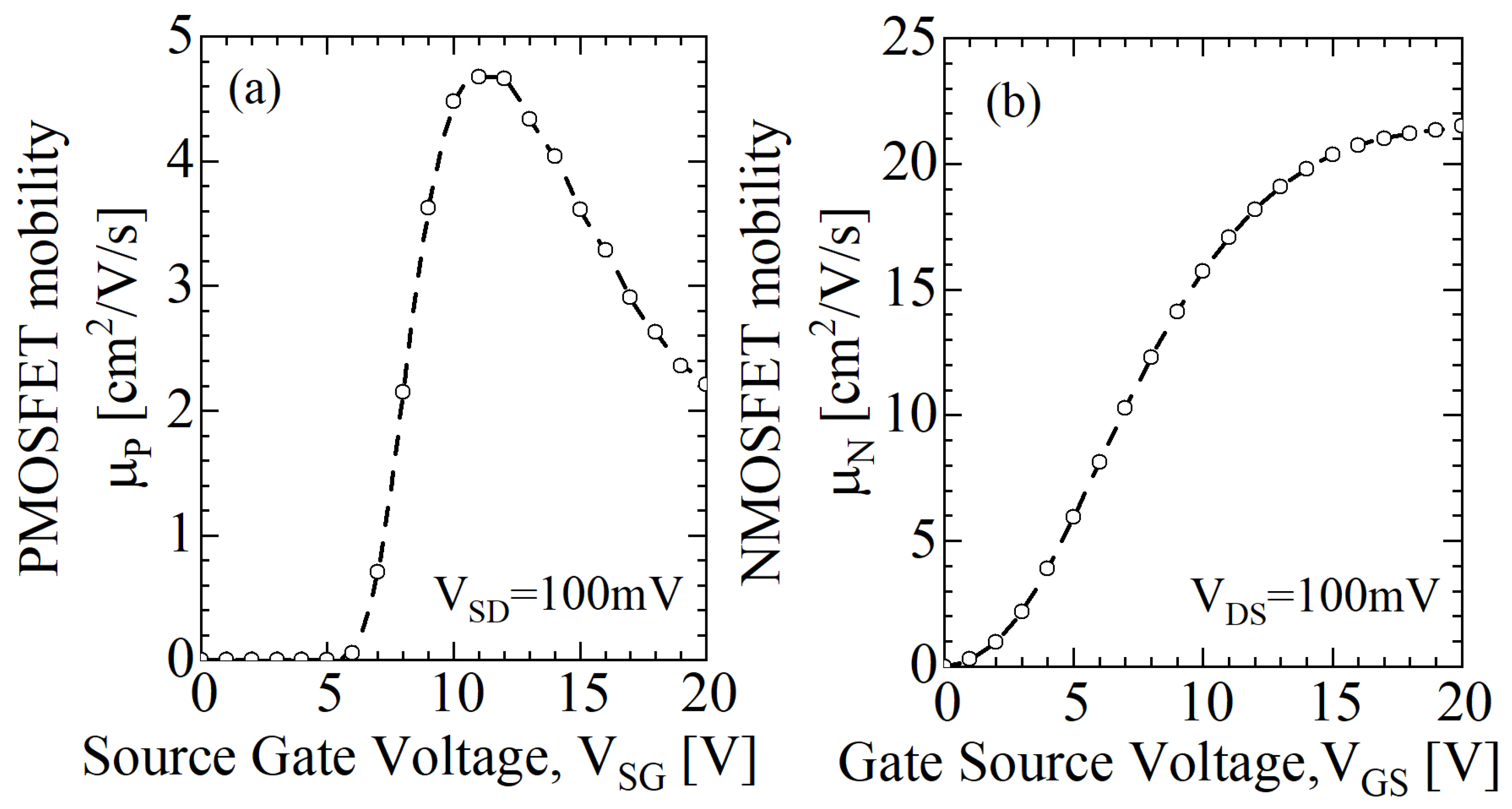
The curves of
Figure A1 at
mV are used to extract both the threshold voltage,
, and the mobility,
. By using the second derivative method [
33], we extracted the threshold voltages reported in
Table A1, whereas the channel mobility dependency on the
is obtained using the following equation:
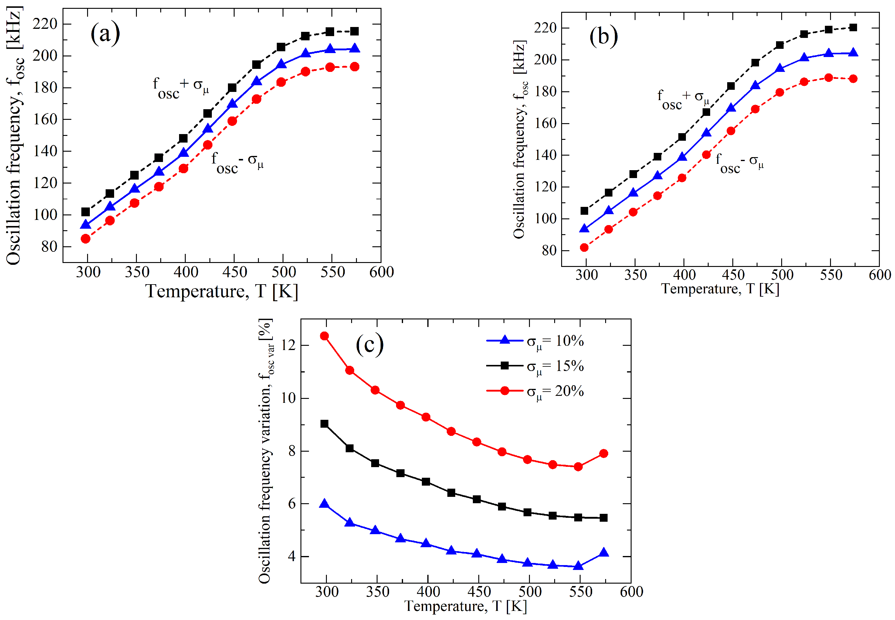
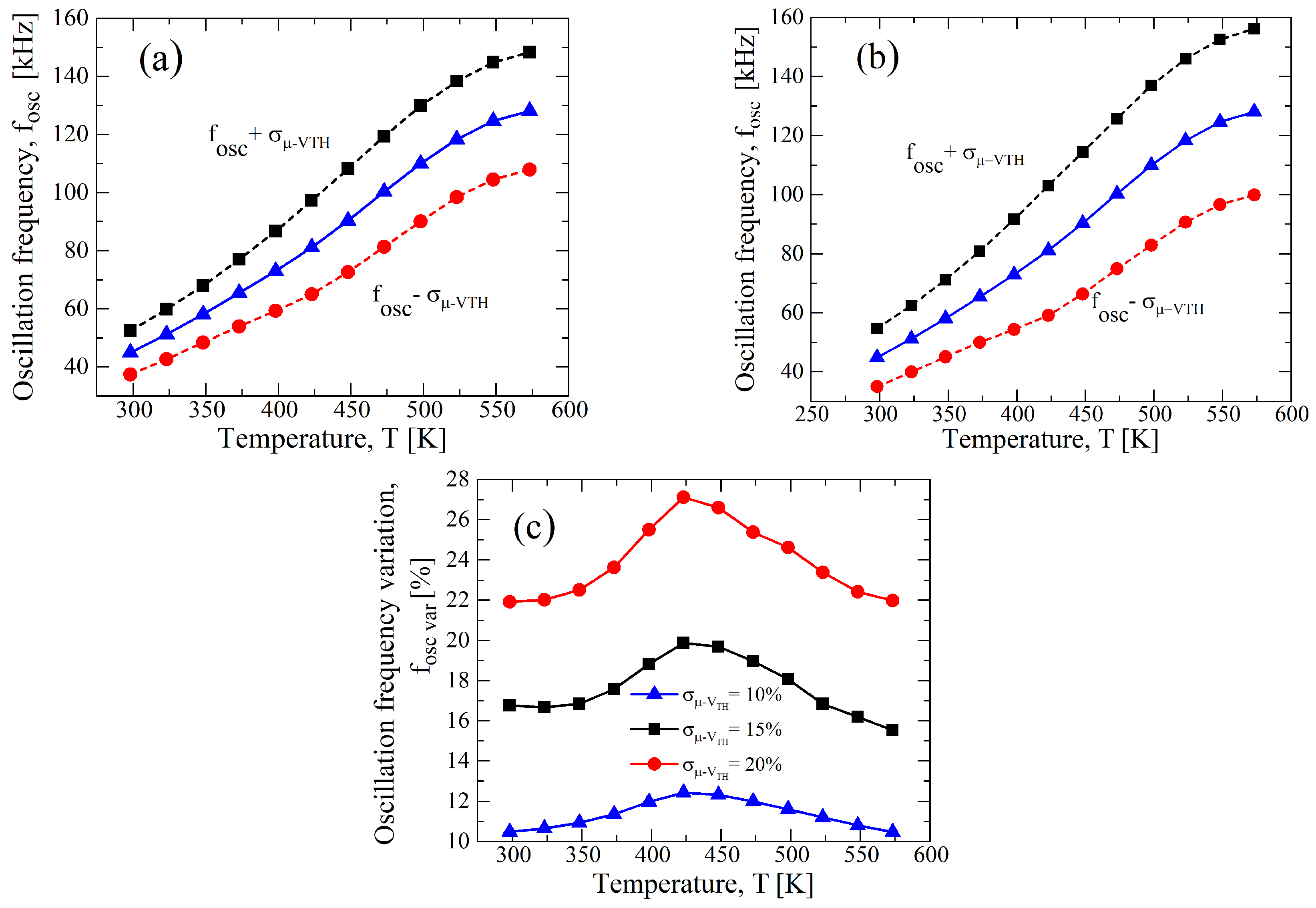
and are reported in
Figure A3a,b for PMOSFET and NMOSFET, respectively. Their mean value is the channel mobility reported in
Table A1 and it is used to design the proposed circuit in
Section 2. In
Figure A3b, the unusual behavior of the NMOSFET channel mobility as a function of
is shown, and it has been described in
Section 3 in order to justify the inconsistency between the expected specification and the numerical simulation results of the design in
Table 2. Indeed, only PMOSFET channel mobility (see
Figure A3a) shows typical step-like behavior, as well as a decrease with the increase in
; instead,
has a continuous increase until it reaches a maximum at around
V.
Figure A3.
Extracted mobility from the transcharacteristics of
Figure A1 by using (
A1) for 4H-SiC. (
a) PMOSFET with
m/10
m and (
b) NMOSFET with
m/10
m at
V,
V, and at r.t.
Figure A3.
Extracted mobility from the transcharacteristics of
Figure A1 by using (
A1) for 4H-SiC. (
a) PMOSFET with
m/10
m and (
b) NMOSFET with
m/10
m at
V,
V, and at r.t.
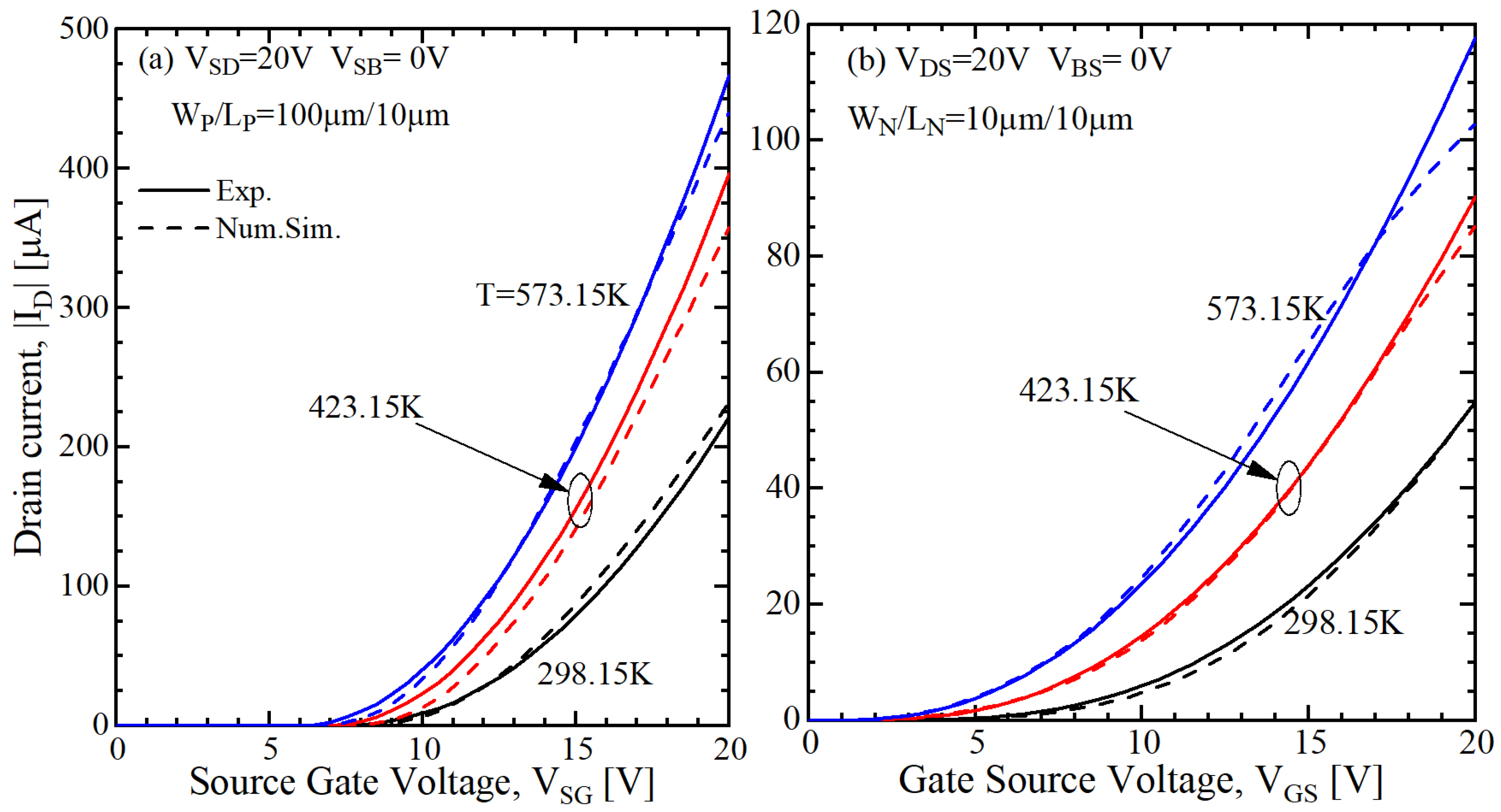
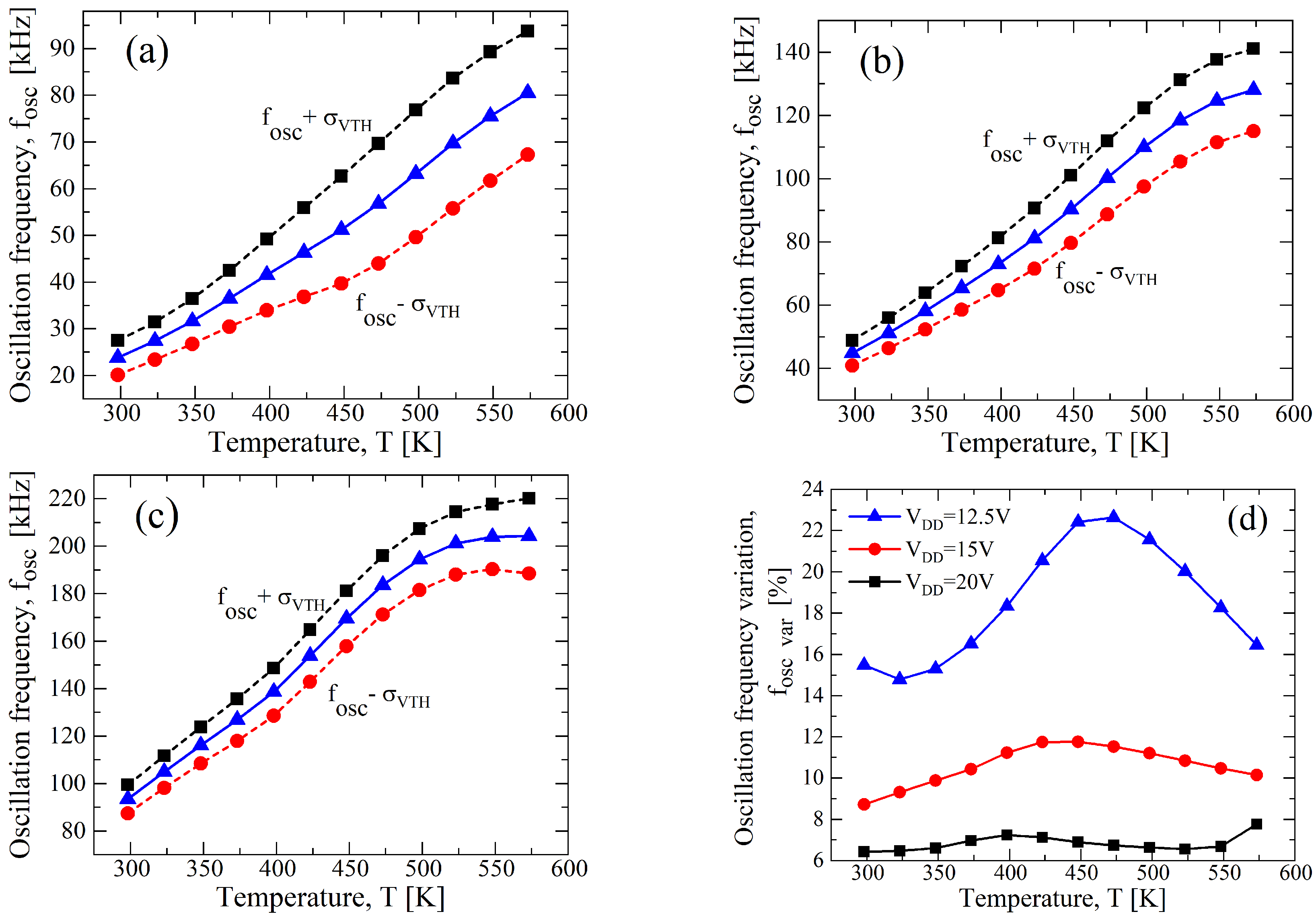
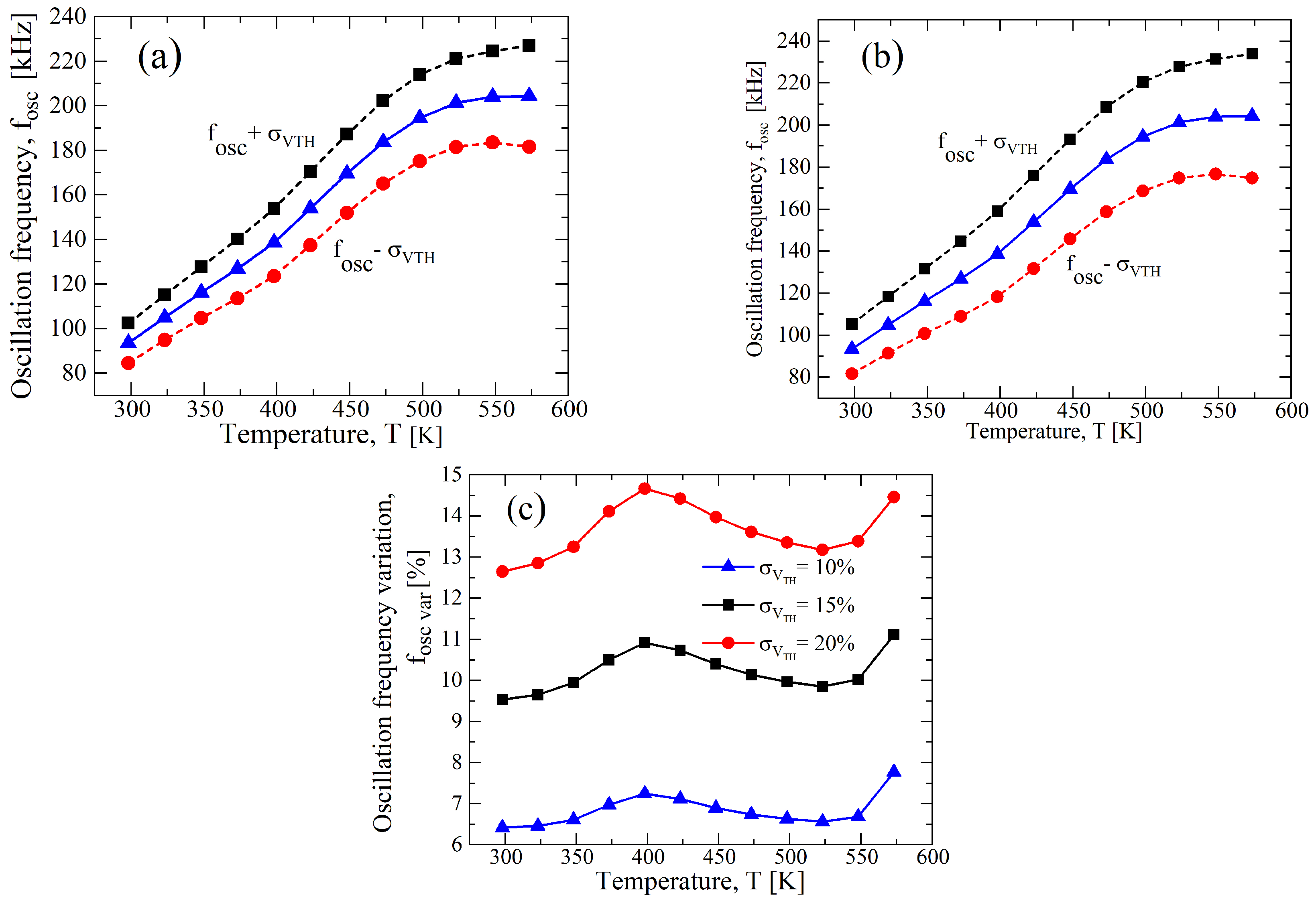
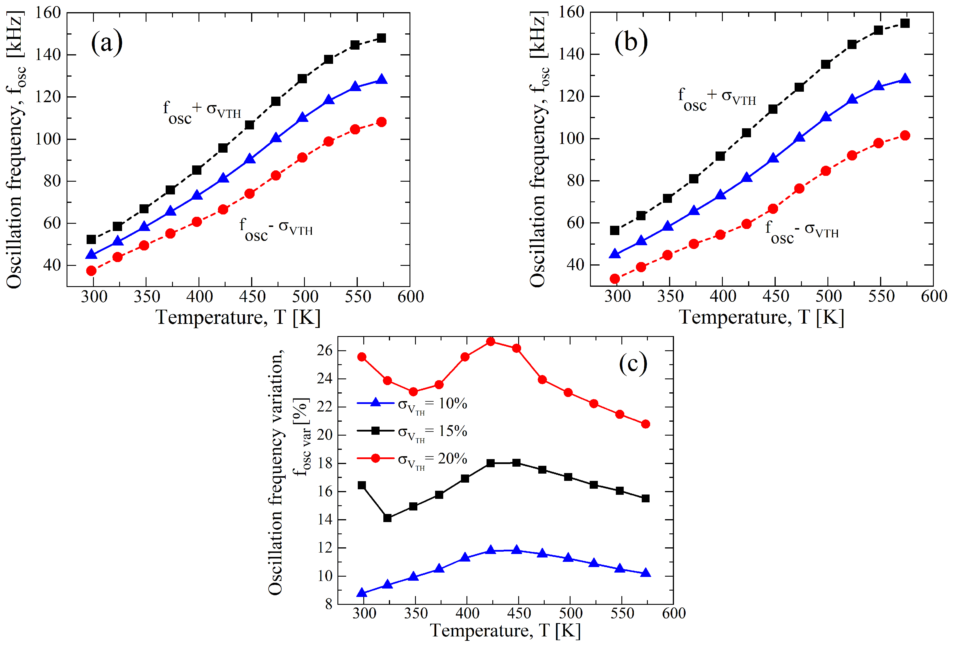
The temperature effect on the transistor currents are reported in
Figure A4 for a
V, and it is clear that the increase in the current with the temperature occurs both for PMOSFET and NMOSFET. Such a behavior is due to a combination of phenomena: on one hand, the channel mobility increases up to 400 K and then decreases, as reported in [
34] for a 4H-SiC lateral NMOS with a bulk doped
cm
; on the other hand, the threshold voltage continuously decreases with the temperature [
35]. In order to take into account such behavior, a temperature dependency of
can be modeled with the following linear function [
24]:
where
is a negative constant and we can neglect it from our analysis in a first approximation, because it is of the order of mV/K; on the other side, the temperature dependency of the channel mobility is modeled as follows [
24,
34]:
where
is a positive fitting parameter and is higher than 1.
It is worth noting that the high density of defects at the
interface is the reason for the improvement in the MOSFETs’ performance with the increase in temperature [
36], whereas 4H-SiC bipolar devices showed worst behaviors under high-temperature operations; in particular, a thermal runaway of the current is observed [
37,
38], limiting their applications under harsh environment conditions.
Figure A4.
Comparison between experimental and Verilog-A numerical model transcharacteristics of lateral 4H-SiC. (a) PMOSFET with m/10 m and (b) NMOSFET with m/10 m at V, V, and for temperature, from 298 K to 573 K.
Figure A4.
Comparison between experimental and Verilog-A numerical model transcharacteristics of lateral 4H-SiC. (a) PMOSFET with m/10 m and (b) NMOSFET with m/10 m at V, V, and for temperature, from 298 K to 573 K.
The numerical simulations performed in Cadence Virtuoso are based on the compact BSIM4SiC model [
22] and they have been opportunely developed by Fraunhofer IISB for the IISB’s 2
m 4H-SiC CMOS technology. It is a extension of the widely used BSIM4 compact model, in which the typical physical phenomena of the 4H-SiC lateral n-channel and p-channel MOSFETs are considered. Indeed, the lower quality of the
interface induces a high density of interface trapped charges, differing significantly, in terms of the transfer and output characteristics, from the Silicon MOSFETs ones.
The effects include mobility degradation, a lower subthreshold slope, soft saturation, and an increase in the flat band and threshold voltages [
22]. For an accurate description of the IISB’s 2
m 4H-SiC CMOS technology, the parameters of the BSIM4SiC model have been determined through a parameter extraction procedure based on the measurement data of n- and p-type transistors. The developed compact model fits the experimental curves quite well, as shown in
Figure A1 and
Figure A2, with a higher accuracy for the NMOSFET case with respect to the PMOSFET case, especially for the output characteristics displayed in
Figure A2a. The modeling of 4H-SiC PMOSFET is generally more challenging, due to the more limited knowledge about the defects at the
interface in the n-type body region with respect to 4H-SiC NMOSFET, which has had much more interest thanks to the power electronics applications. Then, the model also includes channel geometry scaling, which makes the parameter extraction and the achievement of satisfactory results even more complicated for all of the considered geometry. Moreover, in
Figure A4, its validity is shown over a temperature range from 298 K to 573 K.


 ,
, 
