

Dynamic Zero Current Method to Reduce Measurement Error in Low Value Resistive Sensor Array for Wearable Electronics

Abstract
:1. Introduction
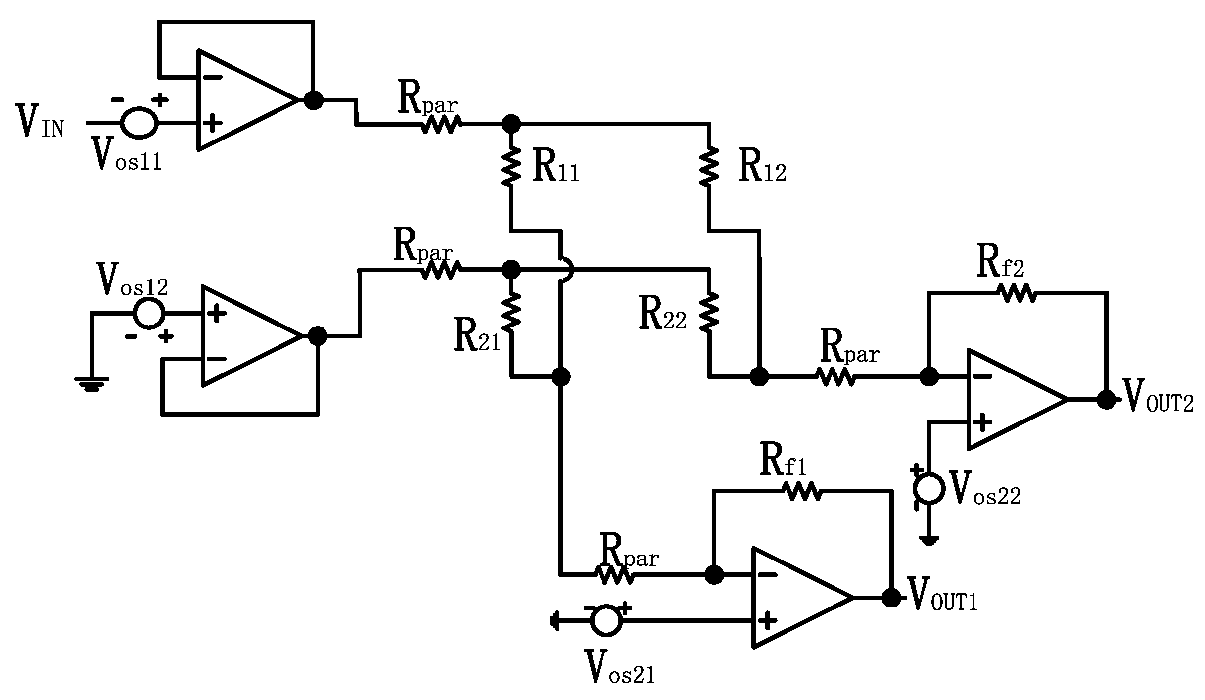
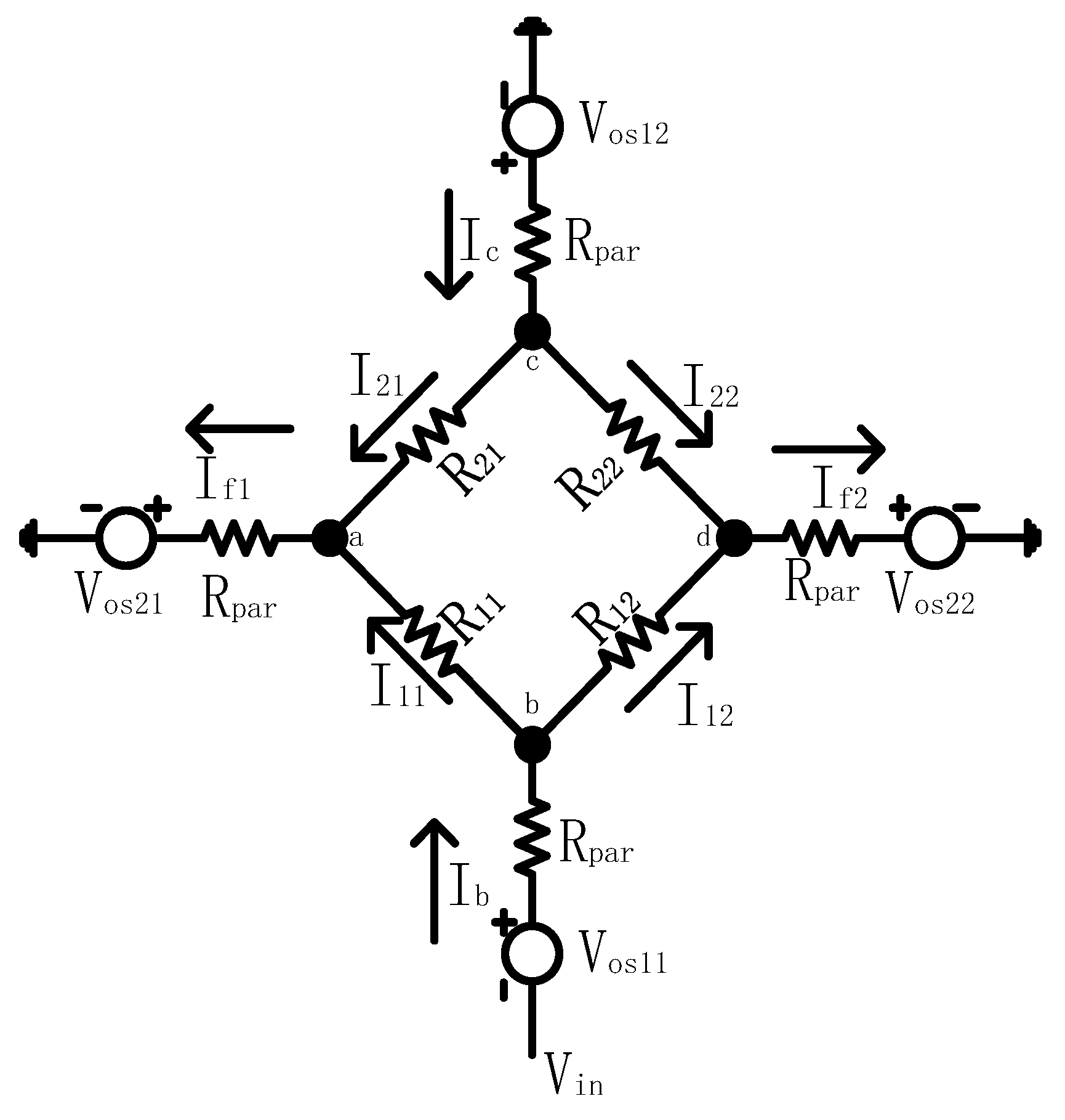
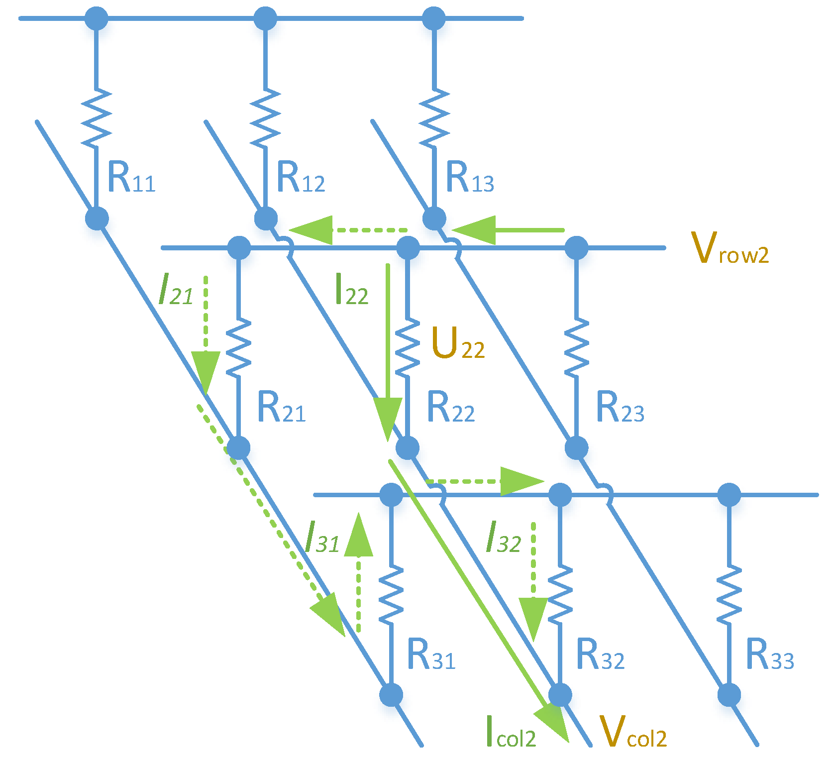
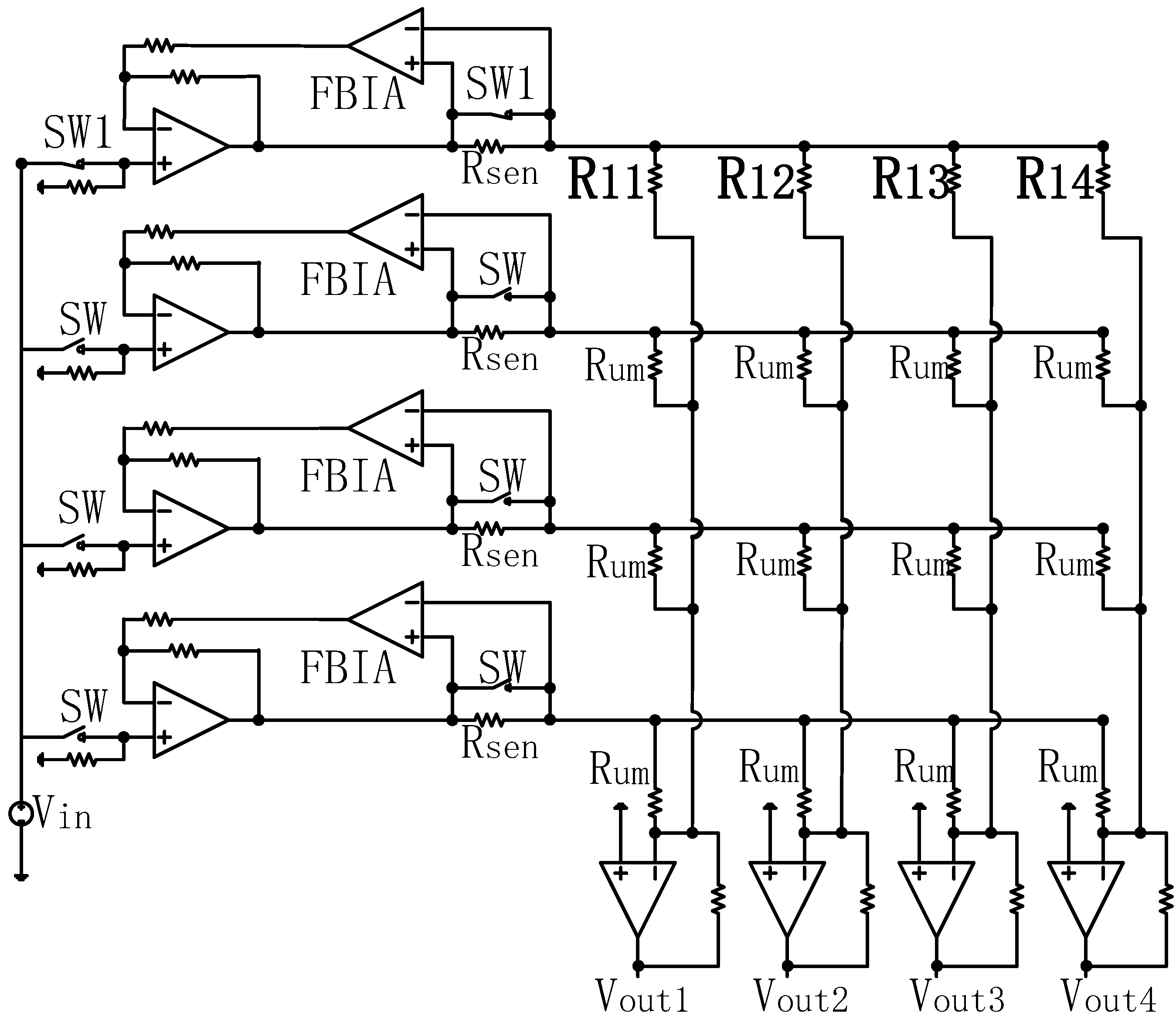
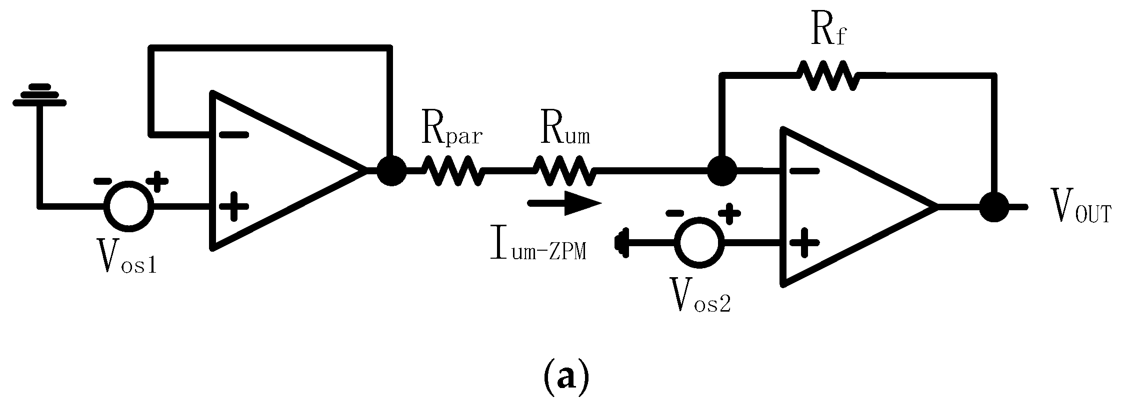
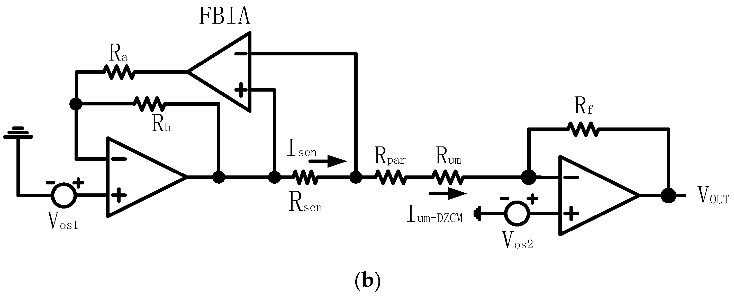
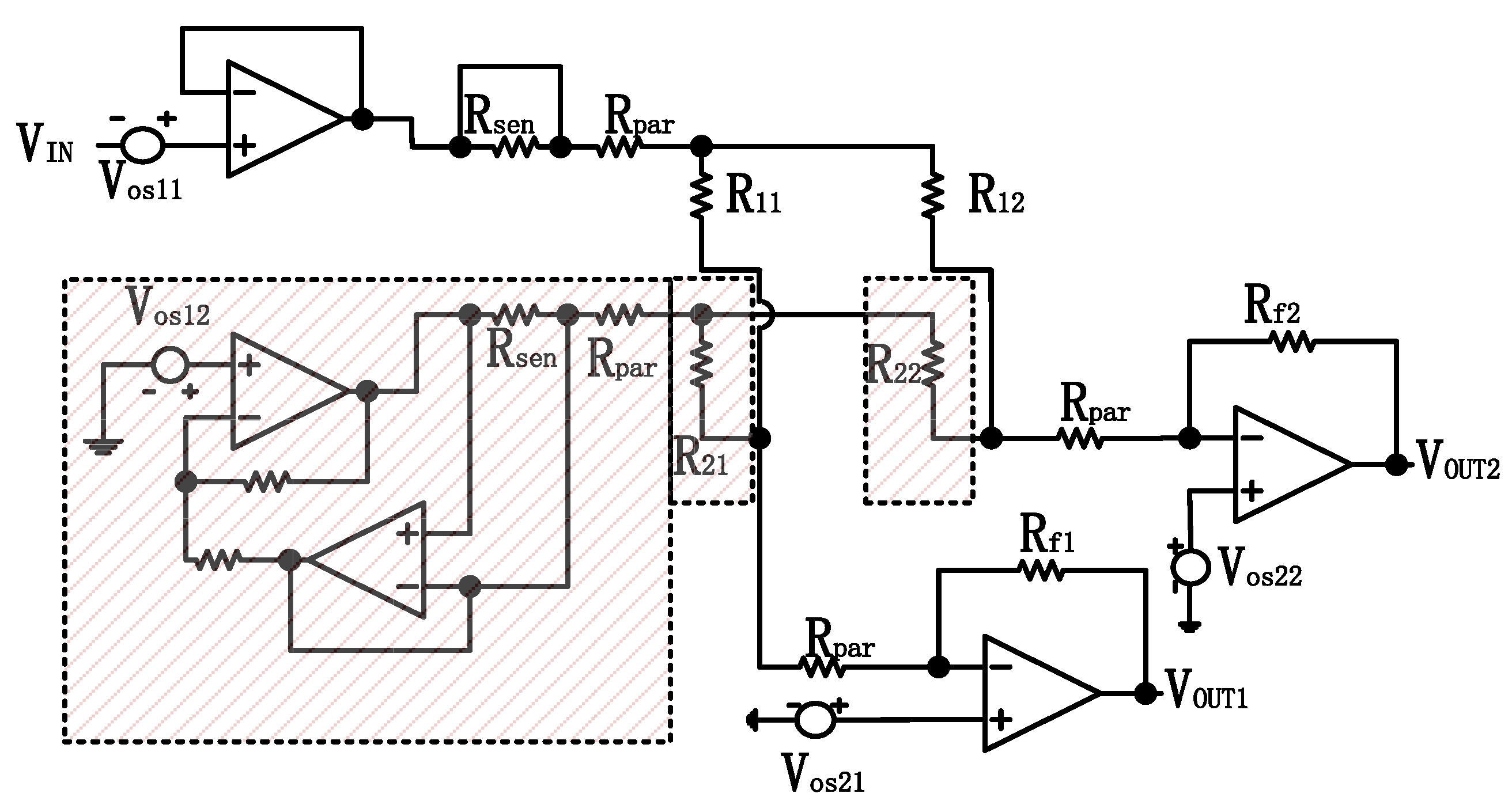
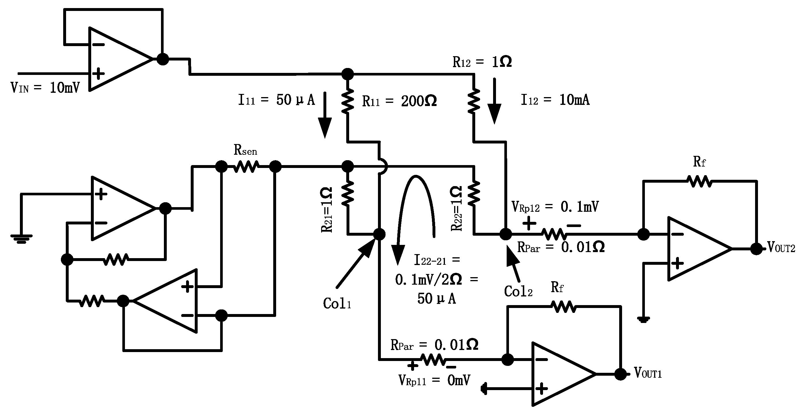
2. Dynamical Zero Current Method
- Parasitic resistance from connection wires and PCB wires contributes a large crosstalk current effect.
- Offset voltage of row and column driving amplifiers induces a crosstalk current effect.
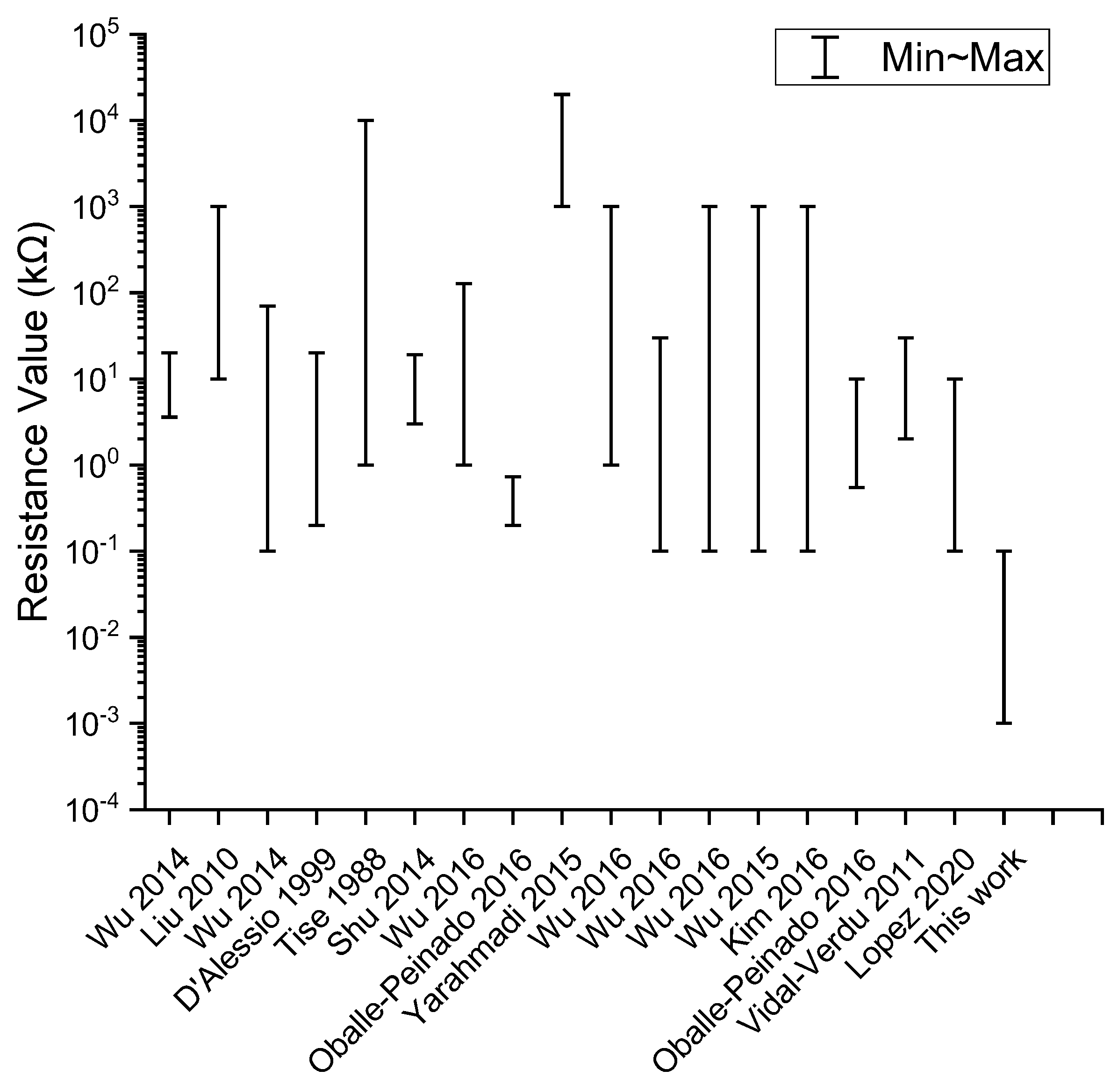
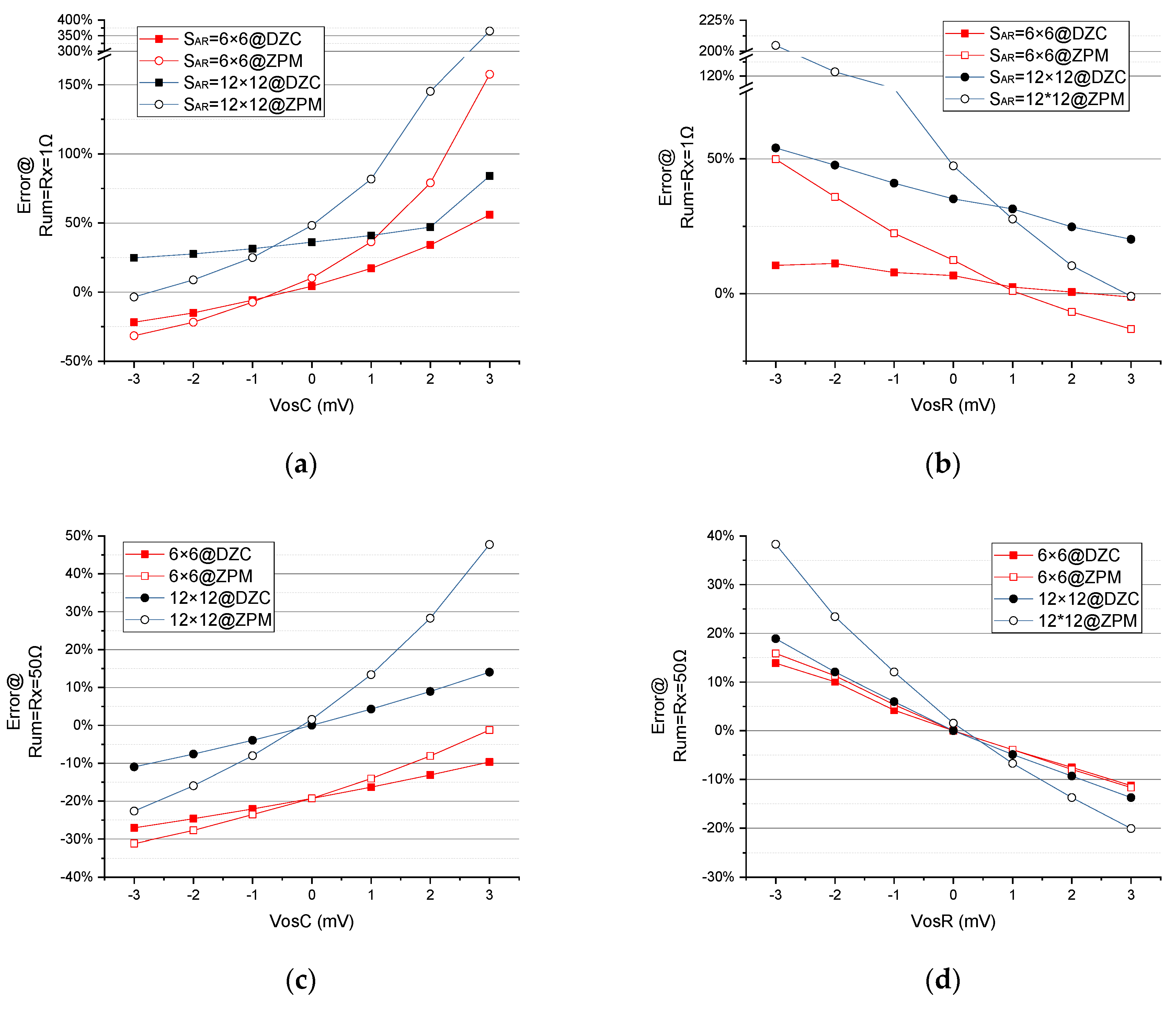
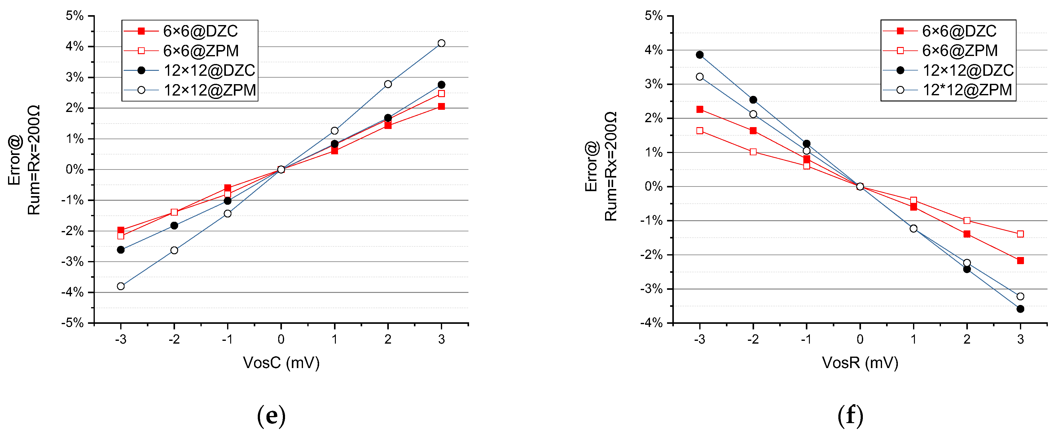
3. Experiments for DZCM/ZPM and Discussion
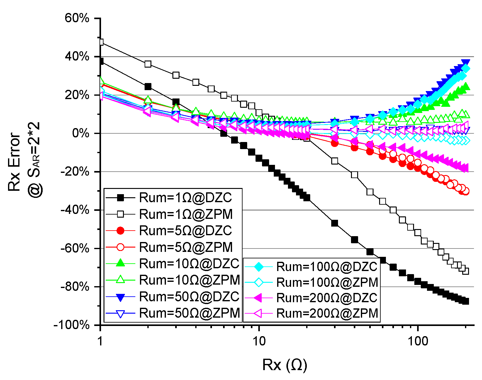
3.1. Experimental Result for DZCM with Ideal Resistors
- i.
- the measurement errors of the DZCM and ZPM are found to be comparable when falls within the range of to . There is no significant improvement on the system performance by the additional feedback network of the DZCM in this range.
- ii.
- As goes beyond to , the e% of the DZCM is noticeably larger than that of the ZPM in all array sizes due to the underlying crosstalk current effect. The crosstalk current in the DZCM feedback network amounts to 25 µA, while the offset voltage of the feedback amplifier ‘AD623′ is 25 µV and the resistance value of the sensing resistor is 1 Ω. This gives rise to an undesired crosstalk current in , as, if and , we will have . Meanwhile, the offset voltage of the ZPM is intentionally and manually compensated to zero to minimize the crosstalk current down to zero. We used an adjustable resistor to form a reference voltage divider and connect it to the positive node of row/column amplifiers, shown as and , as displayed in Figure 4a. The result shows that the ZPM outperforms the DZCM within this range of , i.e., to , with notably smaller measurement error. Nonetheless, this crosstalk current effect in the DZCM can be further suppressed by increasing or in the feedback network.
- i.
- e% of the DZCM is smaller than that of the ZPM within the range of to , showing the advantage of the DZCM feedback network in bringing down the crosstalk current.
- ii.
- As increases from to , measurement error changes from zero to a significant negative value. This unfavorable event also occurs in ZPM circuitry. Moreover, this event occurred in reference [29] Figure 4, Figure 5, Figure 6 and Figure 7 reference [39] Figure 8, reference [21] Figure 9, reference [36] Figure 5, reference [34] Figure 5, reference [30] Figure 9. We name this event the singular values effect (SVE), as it occurs when the measured resistor is tremendously different from the adjacent unmeasured resistors.
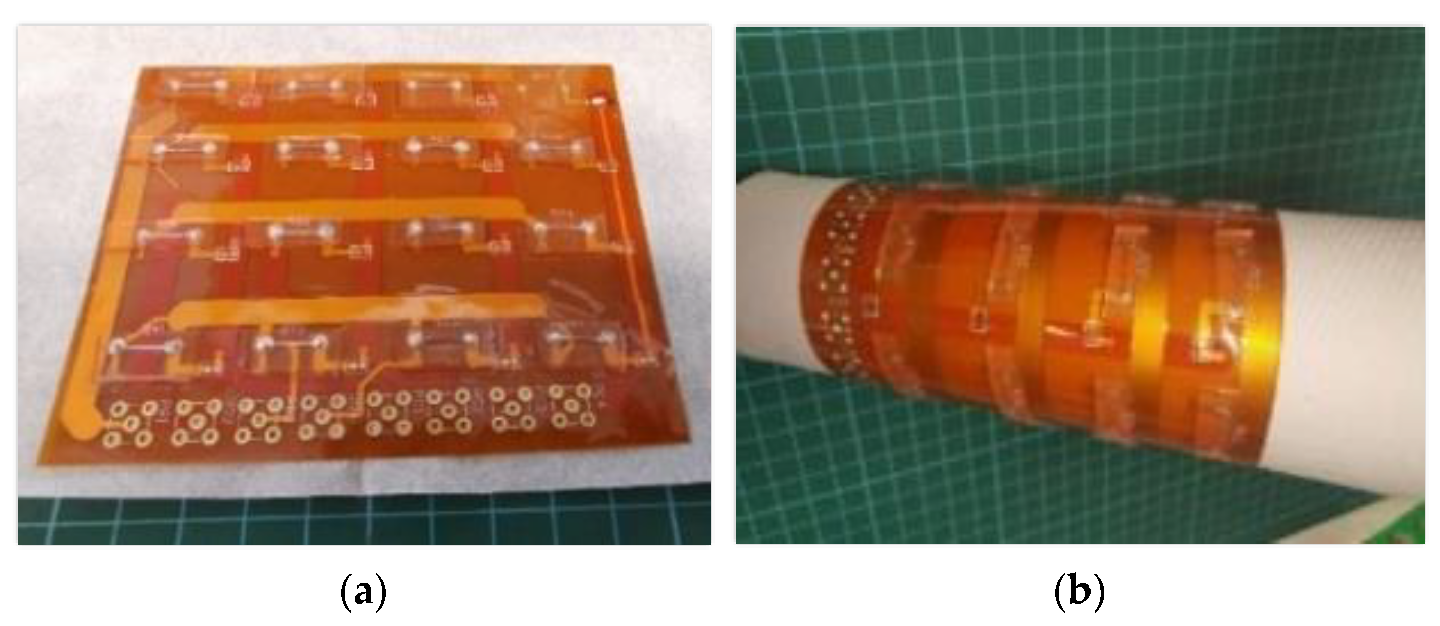
3.2. DZCM and ZPM Application on Liquid Metal EGaIn Based Flexible RSA
- i.
- Single sensor on a flat surface;
- ii.
- single sensor on a curved surface;
- iii.
- RSA with ZPM on a flat surface;
- iv.
- RSA with ZPM on a curved surface;
- v.
- RSA with DZCM on a flat surface;
- vi.
- RSA with DZCM on a curved surface.
3.3. Discussion
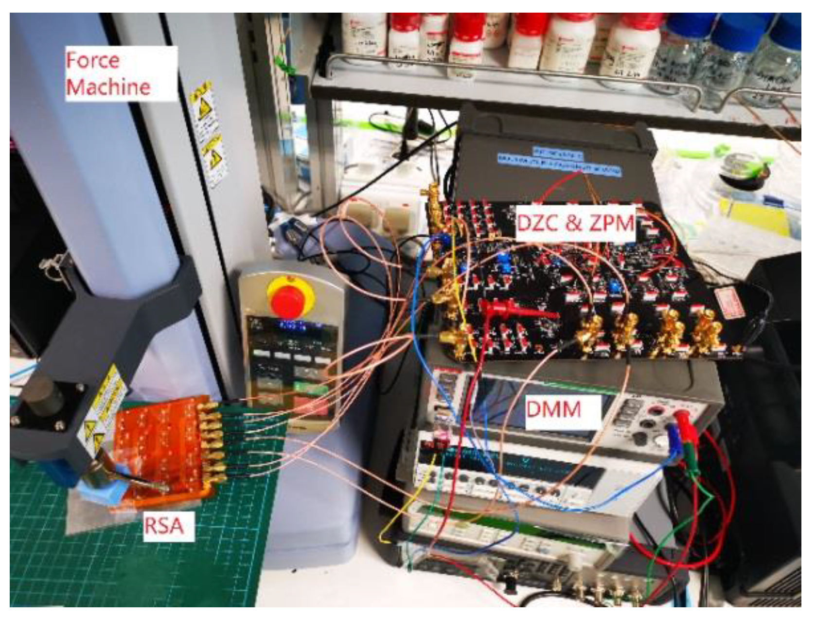
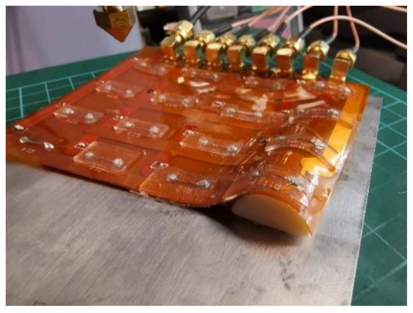
- i.
- Copper wires of 3.6 mm/35 mm/70 µm (width/length/thickness) to connect the resistors to form an RSA on the PCB.
- ii.
- SMA coaxial connector/cable to link RSA PCB to the readout PCB.
- iii.
- Copper wires of 0.15 mm/75 mm/70 µm (width/length/thickness) to connect the SMA connectors and amplifiers on the PCB in the EXP.
- i.
- The larger physical dimensions of an electrical connection lead to lower parasitic resistance. Nevertheless, the use of bulky connecting wires and connectors in wearable systems is not feasible as they defeat the purpose of making an accessory, which is supposed to be comfortable and easy to wear. The DZCM helps to solve this issue as it has higher tolerance for parasitic resistance. In other words, it enables thinner wires and smaller connectors to be used in the wearable.
- ii.
- The input offset voltage of the amplifier varies with the ambient temperature. Consequently, the measurement result is greatly influenced by the operating environment. The input offset voltage also varies in mass production; thus, the measurement result changes with different product batches. By applying the DZCM, that is less sensitive to the fluctuation of the input offset voltage, these issues can be easily resolved.
4. Conclusions
5. Patents
Author Contributions
Funding
Institutional Review Board Statement
Informed Consent Statement
Data Availability Statement
Conflicts of Interest
Appendix A


Appendix B
References
- Dickey, M.D. Stretchable and Soft Electronics using Liquid Metals. Adv. Mater. 2017, 29, 1606425. [Google Scholar] [CrossRef] [PubMed]
- Cheng, S.; Wu, Z. A Microfluidic, Reversibly Stretchable, Large-Area Wireless Strain Sensor. Adv. Funct. Mater. 2011, 21, 2282–2290. [Google Scholar] [CrossRef]
- Roberts, P.; Damian, D.D.; Shan, W.; Lu, T.; Majidi, C. Soft-matter capacitive sensor for measuring shear and pressure deformation. In Proceedings of 2013 IEEE International Conference on Robotics and Automation, Karlsruhe, Germany, 6–10 May 2013; pp. 3529–3534. [Google Scholar] [CrossRef]
- Vogt, D.M.; Park, Y.-L.; Wood, R.J. Design and Characterization of a Soft Multi-Axis Force Sensor Using Embedded Microfluidic Channels. IEEE Sens. J. 2013, 13, 4056–4064. [Google Scholar] [CrossRef] [Green Version]
- Yeo, J.C.; Yu, J.; Koh, Z.M.; Wang, Z.; Lim, C.T. Wearable tactile sensor based on flexible microfluidics. Lab Chip 2016, 16, 3244–3250. [Google Scholar] [CrossRef] [PubMed] [Green Version]
- Yeo, J.C.; Kenry; Yu, J.; Loh, K.P.; Wang, Z.; Lim, C.T. Triple-State Liquid-Based Microfluidic Tactile Sensor with High Flexibility, Durability, and Sensitivity. ACS Sens. 2016, 1, 543–551. [Google Scholar] [CrossRef]
- Yu, L.; Yeo, J.C.; Soon, R.H.; Yeo, T.; Lee, H.H.; Lim, C.T. Highly Stretchable, Weavable, and Washable Piezoresistive Microfiber Sensors. ACS Appl. Mater. Interfaces 2018, 10, 12773–12780. [Google Scholar] [CrossRef]
- Snyder, W.E.; Clair, J.S. Conductive Elastomers as Sensor for Industrial Parts Handling Equipment. IEEE Trans. Instrum. Meas. 1978, 27, 94–99. [Google Scholar] [CrossRef]
- Prutchi, D.; Arcan, M. Dynamic contact stress analysis using a compliant sensor array. Measurement 1993, 11, 197–210. [Google Scholar] [CrossRef]
- Tanaka, A.; Matsumoto, S.; Tsukamoto, N.; Itoh, S.; Chiba, K.; Endoh, T.; Nakazato, A.; Okuyama, K.; Kumazawa, Y.; Hijikawa, M.; et al. Infrared focal plane array incorporating silicon IC process compatible bolometer. IEEE Trans. Electron Devices 1996, 43, 1844–1850. [Google Scholar] [CrossRef]
- Takei, K.; Takahashi, T.; Ho, J.C.; Ko, H.; Gillies, A.G.; Leu, P.W.; Fearing, R.S.; Javey, A. Nanowire active-matrix circuitry for low-voltage macroscale artificial skin. Nat. Mater. 2010, 9, 821–826. [Google Scholar] [CrossRef]
- Wang, C.; Hwang, D.; Yu, Z.; Takei, K.; Park, J.; Chen, T.; Ma, B.; Javey, A. User-interactive electronic skin for instantaneous pressure visualization. Nat. Mater. 2013, 12, 899–904. [Google Scholar] [CrossRef] [PubMed]
- Kane, B.J.; Cutkosky, M.R.; Kovacs, G.T.A. A traction stress sensor array for use in high-resolution robotic tactile imaging. J. Microelectromechanical Syst. 2000, 9, 425–434. [Google Scholar] [CrossRef]
- Vidal-Verdú, F.; Oballe-Peinado, Ó.; Sánchez-Durán, J.A.; Castellanos-Ramos, J.; Navas-González, R. Three realizations and comparison of hardware for piezoresistive tactile sensors. Sensors 2011, 11, 3249–3266. [Google Scholar] [CrossRef] [Green Version]
- Oballe-Peinado, Ó.; Vidal-Verdú, F.; Sánchez-Durán, J.A.; Castellanos-Ramos, J.; Hidalgo-López, J.A. Accuracy and resolution analysis of a direct resistive sensor array to FPGA interface. Sensors 2016, 16, 181. [Google Scholar] [CrossRef] [PubMed] [Green Version]
- Oballe-Peinado, Ó.; Vidal-Verdú, F.; Sánchez-Durán, J.A.; Castellanos-Ramos, J.; Hidalgo-López, J.A. Improved circuits with capacitive feedback for readout resistive sensor arrays. Sensors 2016, 16, 149. [Google Scholar] [CrossRef] [Green Version]
- Shu, L.; Tao, X.; Feng, D.D. A new approach for readout of resistive sensor arrays for wearable electronic applications. IEEE Sens. J. 2014, 15, 442–452. [Google Scholar] [CrossRef]
- Hidalgo-Lopez, J.A.; Romero-Sánchez, J.; Fernández-Ramos, R. New approaches for increasing accuracy in readout of resistive sensor arrays. IEEE Sens. J. 2017, 17, 2154–2164. [Google Scholar] [CrossRef]
- López, J.A.H.; Oballe-Peinado, Ó.; Sánchez-Durán, J.A. A proposal to eliminate the impact of crosstalk on resistive sensor array readouts. IEEE Sens. J. 2020, 20, 13461–13470. [Google Scholar] [CrossRef]
- Lorussi, F.; Rocchia, W.; Scilingo, E.P.; Tognetti, A.; De Rossi, D. Wearable, redundant fabric-based sensor arrays for reconstruction of body segment posture. IEEE Sens. J. 2004, 4, 807–818. [Google Scholar] [CrossRef]
- Tise, B. A compact high resolution piezoresistive digital tactile sensor. In Proceedings of the 1988 IEEE International Conference on Robotics and Automation, Philadelphia, PA, USA, 24–29 April 1988; pp. 760–764. [Google Scholar] [CrossRef]
- Speeter, T.H. Flexible, piezoresitive touch sensing array. In Proceedings of the Optics, Illumination, and Image Sensing for Machine Vision III, Boston, MA, USA, 7–11 November 1988; pp. 31–43. [Google Scholar]
- Speeter, T.H. A tactile sensing system for robotic manipulation. Int. J. Robot. Res. 1990, 9, 25–36. [Google Scholar] [CrossRef]
- Liu, H.; Zhang, Y.-F.; Liu, Y.-W.; Jin, M.-H. Measurement errors in the scanning of resistive sensor arrays. Sens. Actuators A Phys. 2010, 163, 198–204. [Google Scholar] [CrossRef]
- D’Alessio, T. Measurement errors in the scanning of piezoresistive sensors arrays. Sens. Actuators A Phys. 1999, 72, 71–76. [Google Scholar] [CrossRef]
- Jianfeng, W.; Lei, W.; Jianqing, L.; Zhongzhou, Y. A small size device using temperature sensor array. Chin. J. Sens. Actuators 2011, 24, 1649–1652. [Google Scholar]
- Wu, J.; Wang, L.; Li, J. Design and crosstalk error analysis of the circuit for the 2-D networked resistive sensor array. IEEE Sens. J. 2014, 15, 1020–1026. [Google Scholar] [CrossRef]
- Wu, J.; Wang, L.; Li, J.; Song, A. A novel crosstalk suppression method of the 2-D networked resistive sensor array. Sensors 2014, 14, 12816–12827. [Google Scholar] [CrossRef] [PubMed] [Green Version]
- Wu, J.; He, S.; Li, J.; Song, A. Cable crosstalk suppression with two-wire voltage feedback method for resistive sensor array. Sensors 2016, 16, 253. [Google Scholar] [CrossRef] [PubMed] [Green Version]
- Wu, J.; Wang, L.; Li, J. General voltage feedback circuit model in the two-dimensional networked resistive sensor array. J. Sens. 2015, 2015, 913828. [Google Scholar] [CrossRef] [Green Version]
- Lazzarini, R.; Magni, R.; Dario, P. A tactile array sensor layered in an artificial skin. In Proceedings of the 1995 IEEE/RSJ International Conference on Intelligent Robots and Systems. Human Robot Interaction and Cooperative Robots, Pittsburgh, PA, USA, 5–9 August 1995; pp. 114–119. [Google Scholar] [CrossRef]
- Saxena, R.S.; Bhan, R.K.; Saini, N.K.; Muralidharan, R. Virtual ground technique for crosstalk suppression in networked resistive sensors. IEEE Sens. J. 2010, 11, 432–433. [Google Scholar] [CrossRef]
- Yarahmadi, R.; Safarpour, A.; Lotfi, R. An improved-accuracy approach for readout of large-array resistive sensors. IEEE Sens. J. 2015, 16, 210–215. [Google Scholar] [CrossRef]
- Wu, J.; Wang, L. Cable crosstalk suppression in resistive sensor array with 2-wire S-NSDE-EP method. J. Sens. 2016, 2016, 8051945. [Google Scholar] [CrossRef] [Green Version]
- Kim, J.-S.; Kwon, D.-Y.; Choi, B.-D. High-accuracy, compact scanning method and circuit for resistive sensor arrays. Sensors 2016, 16, 155. [Google Scholar] [CrossRef] [PubMed] [Green Version]
- Wu, J.; Wang, Y.; Li, J.; Song, A. A novel two-wire fast readout approach for suppressing cable crosstalk in a tactile resistive sensor array. Sensors 2016, 16, 720. [Google Scholar] [CrossRef] [PubMed] [Green Version]
- Wu, J.; Li, J. Approximate model of zero potential circuits for the 2-D networked resistive sensor array. IEEE Sens. J. 2016, 16, 3084–3090. [Google Scholar] [CrossRef]
- Manapongpun, P.; Bunnjaweht, D. An Enhanced Measurement Circuit for Piezoresistive Pressure Sensor Array. In Proceedings of the 2020 17th International Conference on Electrical Engineering/Electronics, Computer, Telecommunications and Information Technology (ECTI-CON), Phuket, Thailand, 24–27 June 2020; pp. 105–108. [Google Scholar] [CrossRef]
- Warnakulasuriya, A.S.; Dinushka, N.Y.; Dias, A.A.C.; Ariyarathna, H.P.A.R.; Ramraj, C.; Jayasinghe, S.; Silva, A.C.D. A Readout Circuit Based on Zero Potential Crosstalk Suppression for a Large Piezoresistive Sensor Array: Case Study Based on a Resistor Model. IEEE Sens. J. 2021, 21, 16770–16779. [Google Scholar] [CrossRef]
- Hu, Z.; Tan, W.; Kanoun, O. High Accuracy and Simultaneous Scanning AC Measurement Approach for Two-Dimensional Resistive Sensor Arrays. IEEE Sens. J. 2019, 19, 4623–4628. [Google Scholar] [CrossRef]
- Wu, J.-F.; Li, J.-Q.; Song, A.-G. Readout circuit based on double voltage feedback loops in the two-dimensional resistive sensor array: Design, modelling and simulation evaluation. IET Sci. Meas. Technol. 2017, 11, 288–296. [Google Scholar] [CrossRef]


| EXP A (Rpar = 0 Ω, vOS = 0 mV) | EXP B (Rpar = 0 Ω, vOS = 0 mV, SAR = 2 × 2) | EXP C (vOS = 0 mV) | EXP D (Rpar = 0 Ω) | |||||||
|---|---|---|---|---|---|---|---|---|---|---|
| Rx (Ω) | Rum (Ω) | SAR | Rx (Ω) | Rum (Ω) | Rx = Rum (Ω) | RparCol RparRow (Ω) | SAR | Rx = Rum (Ω) | SAR | vOS (mV) |
| 1 to 10, step = 1. 10 to 20, step = 1. 20 to 100, step = 10. 100 to 200, step = 10. | 1 200 | 2 × 2 4 × 4 8 × 8 | 1 to 10, step = 1. 10 to 20, step = 1. 20 to 100, step = 10. 100 to 200, step = 10. | 1 5 10 50 100 200 | 1 50 200 | 0, 0.5 1,1.5 2, 2.5 3, 3.5 | 6 × 6 12 × 12 | 1 50 200 | 6 × 6 12 × 12 | 0 ±1.0 ±2.0 ±3.0 |
| Array Size | |||||
|---|---|---|---|---|---|
| DZCM | ZPM | DZCM | ZPM | ||
| 1 | 6×6 | 1.83 | 9.82 | 12.16 | 29.55 |
| 12×12 | 4.18 | 25.37 | 7.32 | 45.45 | |
| 50 | 6×6 | 3.59 | 3.93 | 3.08 | 5.30 |
| 12×12 | 4.66 | 8.34 | 3.57 | 10.05 | |
| 200 | 6×6 | 0.63 | 0.43 | 0.58 | 0.66 |
| 12×12 | 1.06 | 0.92 | 0.77 | 1.13 | |
Disclaimer/Publisher’s Note: The statements, opinions and data contained in all publications are solely those of the individual author(s) and contributor(s) and not of MDPI and/or the editor(s). MDPI and/or the editor(s) disclaim responsibility for any injury to people or property resulting from any ideas, methods, instructions or products referred to in the content. |
© 2023 by the authors. Licensee MDPI, Basel, Switzerland. This article is an open access article distributed under the terms and conditions of the Creative Commons Attribution (CC BY) license (https://creativecommons.org/licenses/by/4.0/).
Share and Cite
Zhang, H.; Teoh, J.C.; Wu, J.; Yu, L.; Lim, C.T. Dynamic Zero Current Method to Reduce Measurement Error in Low Value Resistive Sensor Array for Wearable Electronics. Sensors 2023, 23, 1406. https://doi.org/10.3390/s23031406
Zhang H, Teoh JC, Wu J, Yu L, Lim CT. Dynamic Zero Current Method to Reduce Measurement Error in Low Value Resistive Sensor Array for Wearable Electronics. Sensors. 2023; 23(3):1406. https://doi.org/10.3390/s23031406
Chicago/Turabian StyleZhang, Huanqian, Jee Chin Teoh, Jianfeng Wu, Longteng Yu, and Chwee Teck Lim. 2023. "Dynamic Zero Current Method to Reduce Measurement Error in Low Value Resistive Sensor Array for Wearable Electronics" Sensors 23, no. 3: 1406. https://doi.org/10.3390/s23031406