Abstract
This article proposes a novel fixed-frequency beam scanning leakage antenna based on a liquid crystal metamaterial (LCM) and adopting a metal column embedded microstrip line (MCML) transmission structure. Based on the microstrip line (ML) transmission structure, it was observed that by adding two rows of metal columns in the dielectric substrate, electromagnetic waves can be more effectively transmitted to reduce dissipation, and attenuation loss can be lowered to improve energy radiation efficiency. This antenna couples TEM mode electromagnetic waves into free space by periodically arranging 72 complementary split ring resonators (CSRRs). The LC layer is encapsulated in the transmission medium between the ML and the metal grounding plate. The simulation results show that the antenna can achieve a 106° continuous beam turning from reverse −52° to forward 54° at a frequency of 38 GHz with the holographic principle. In practical applications, beam scanning is achieved by applying a DC bias voltage to the LC layer to adjust the LC dielectric constant. We designed a sector-blocking bias feeder structure to minimize the impact of RF signals on the DC source and avoid the effect of DC bias on antenna radiation. Further comparative experiments revealed that the bias feeder can significantly diminish the influence between the two sources, thereby reducing the impact of bias voltage introduced by LC layer feeding on antenna performance. Compared with existing approaches, the antenna array simultaneously combines the advantages of high frequency band, high gain, wide beam scanning range, and low loss.
1. Introduction
Antennas are vital in wireless communication, transmitting and receiving electromagnetic waves [1,2,3,4,5,6]. Different applications require various antenna functionalities, among which beam scanning performance is crucial to the system function [7,8,9,10]. Since the 1940s, the leaky-wave antenna has garnered significant attention due to its exceptional radiation characteristics and impressive beam scanning capability [11,12,13]. Recently, various leaky-wave antennas have emerged, offering advantages such as high efficiency, low profile, compact size, and simplified feed structure [14,15]. Nevertheless, conventional leaky-wave antennas are limited to frequency beam scanning, which restricts their usability in scenarios with limited spectrum resources. Therefore, there is a need to explore fixed-frequency beam scanning leakage antennas [16,17,18,19,20].
Two methods are commonly used in the production of fixed-frequency beam-scanning leakage antennas, i.e., loading active devices and utilizing tunable materials. The active device loading method mainly uses PIN diodes and varactor diodes [21,22,23,24]. The diode based fixed-frequency scanning leakage antenna has the advantages of stable electromagnetic performance and low cost, but its main disadvantage is that it is not used in high frequency bands, and it cannot be used in millimeter bands or even higher frequency bands. Tunable materials include ferrite, graphene, and LC materials. Nil Apaydin and other scholars proposed a fixed-frequency scanning leakage antenna based on ferrite [25], which achieves beam scanning by applying a static magnetic field at 1.79 GHz. The scanning angle can reach 80°. However, this antenna has a large volume, high power consumption, and a complex external magnetic field structure, which is not conducive to system integration. Esquius Morote proposed a sine modulated graphene leakage antenna with fixed-frequency beam-scanning capability. The antenna operates at terahertz frequencies and sinusoidally modulates the surface reactance of graphene through the field effect of graphene, providing multifunctional beam scanning capability [26]. However, most graphene-based antennas are currently in the theoretical stage, and their electrical modulation characteristics can only be used in terahertz frequency bands [27,28,29]. LC materials are gaining popularity, as they make fixed-frequency beam scanning possible when used in conjunction with leaky-wave antennas [30,31,32]. This is due to the fact that, compared with other electronically controlled materials, LC materials can be utilized from Ku-band all the way up to the optical band, and the insertion loss decreases as the frequency band rises. Therefore, LC materials have shown promise in the design of high-frequency microwave devices [25,33,34]. Significant progress has been made in single-beam scanning leaky-wave antennas using LC materials [35,36,37,38]. In the initial stage, the gain of beam-scanning leakage antennas based on LC materials is primarily low. Yan Gao proposed an electron beam scanning leakage antenna based on composite left- and right-handed rectangular waveguides, operating at 9.7 GHz and offering a beam scanning range of −19 ° to 12° [39]. Yaling Liu designed an LC-based leakage antenna featuring 13 rectangular slits, operating at 10.4 GHz, with a beam pointing range from 30° to 60° and a gain of up to 5 dB [40]. Feng Gao developed a microstrip line cell with LCs, operating at 19.8 GHz and 21.8 GHz. This design yielded a holographic metamaterial antenna with reconfigurable directional maps thanks to the periodic arrangement of 16 cells. The antenna offered a scanning range of −25° to 60° and a gain of up to 8 dB [41].
Subsequent researchers have focused on beam gain and achieved high-gain beam scanning. The authors of [42] used a half-mode comb substrate integrated waveguide circuit as a leaky transmission line, achieving beam scanning from 2° to 20° at 21.5 GHz with a peak gain of up to 12 dB. While their technology has a high gain, the beam scanning range remains narrow, and the operating frequency band is limited. With further development, the operating frequency of leakage antennas is progressing toward higher frequency bands, resulting in numerous notable research achievements. Qi Liu designed an LC-based beam-scanning ML leakage antenna comprising 64 units operating at 30 GHz. This design achieved beam scanning from −27° to 38°, with a gain ranging from 9.5 dB to 12.5 dB [43]. However, the scanning range of the leakage antenna was narrow. Weiyi Zhang proposed an LC substrate integrated waveguide leakage antenna based on holographic theory, operating at 35 GHz. This design achieved a beam scanning range from −45° to 51°, with a maximum gain exceeding 9 dBi and a reflection coefficient below −10 dB [44]. A microstrip line leakage antenna based on the etched complementary open resonant ring of LC materials is proposed in [45]. The antenna works in the Ka-band, and by arranging 56 antenna units to form a periodic leakage antenna, it can achieve a scanning angle between −53° and 60° at 34.7 GHz, and the gain can reach 12.63 dB.
Current research on beam scanning leakage antennas based on LC materials has achieved an excellent level; these advances have the advantages of wide beam scanning range, high gain, and high-frequency band. The authors of [45] achieved excellent beam scanning performance. Low attenuation loss transmission of electromagnetic waves was accomplished by embedding two rows of metal columns in the medium on the basis of a traditional ML transmission structure. However, that study did not consider the bias feeder problem introduced by the LC layer feed, only illustrating that the bias feed has a negligible effect; as such, those authors did not further investigate how much the antenna radiation performance was affected by the LC layer feed voltage. In this article, we follow the transmission structure proposed in this thesis. To realize the feeding of the LC layer more conveniently, we encapsulated the LC layer in the transmission medium of the microstrip line and the metal ground plane. Introducing a bias feeder on the ML [43,46] forms a voltage difference with the metal grounding plate, thus allowing voltage control of the LC layer. To further minimize the impact of the introduced bias voltage on the RF source and the radiation performance of the antenna, we adopted a sector-blocking bias feed structure [47,48]. This structure can significantly reduce the influence between the two sources, thus reducing the impact of the bias voltage introduced due to the LC feed on the antenna performance.
2. Liquid Crystal and Holographic Antenna Principle
2.1. Liquid Crystal
LC is a kind of organic compound between a crystal and a liquid, with both the fluidity of liquid and the anisotropy of crystal [49]. When DC voltage or low-frequency AC voltage is applied to both ends of the LC layer, the long-axis direction of the LC molecules will change, as will the dielectric constant of the LC [50]. When the electromagnetic wave passes through the LC layer as the transmission medium of a microwave device, the transmission characteristics of the electromagnetic wave will change with the change of voltage, thereby changing the transmission characteristics of the electromagnetic wave.
There are many ways to categorize LC materials. According to the difference in how the molecules are arranged within the LC, LC materials can be classified into three types: nematic LCs, near-crystalline LCs, and cholesteric LCs. Nematic LCs are composed of polar rod-shaped molecules with a dipole moment. The center of gravity of each LC molecule has no rules, so the mutual binding between molecules is relatively small, the viscosity is low, and it is easy to rotate under external force [51]. In the design of microwave millimeter waves, nematic LCs are usually selected. The LC material chosen in the design of this paper was also a nematic LC. The electromagnetic properties (behavior) of nematic LCs are modelled as vectors [52,53,54]:
where the unit vector , called the director, represents the average orientation of LC molecules, is the transposition of , is the LC dielectric permittivity tensor, is the identity matrix, and () is the LC complex permittivity felt by the perpendicular (parallel) electric field component to the director. The complex permittivities are:
where are the LC loss tangents. The tuning ability of the microwave device depends not only on its design but also mainly on the degree of the tuning ability of the tunable material. Generally, the absolute and relative tuning abilities of LC material are defined as:
Table 1 shows the parameters of different nematic LC materials at room temperature (20 °C). This paper adopted the No. GT3-23001 LC material with a more extensive tuning range. The relative dielectric constant of the LC material can be changed from 2.5 to 3.3 under applied voltage.

Table 1.
Parameters of different LC models.
2.2. Holographic Antenna Principle
Beam scanning may be realized based on the holographic antenna principle [55]. Holographic technology was first used in optics; it is a kind of light that records all the information about an object and can restore an image of the object’s technology. Holographic technology mainly includes shooting and imaging, i.e., two processes. Shooting uses reference light and object light interference in the holographic film to record all the information. Imaging refers to the use of reference light to irradiate the holographic film process. Due to the diffraction phenomenon of light, the reference light can be restored to the original image of the object through a holographic film. The primary focus of holographic antenna design is to generate a holographic image that records the information of the target wave. The target wave can be restored by illuminating the holographic image with a reference wave source [56,57]. The reference wave equation, target wave equation, and interference wave equation for energy recording can respectively be expressed as follows:
where represents the position information of the recording point on the holographic structure, represents the propagation constant of the reference wave, and represents the propagation constant of the object wave, which is the free-space propagation constant. represents the beam direction of the object wave, which is the expected beam direction.
The holographic antenna principle is a technique that achieves the desired beam pointing by combining the amplitude-weighting technique, which assigns a weighted value to each antenna element based on its contribution to the expected beam direction. By varying the radiated energy of each antenna element, the cells that contribute to the expected beam direction are given a higher radiated power, while those that do not contribute are given a lower radiated power. This may be achieved by taking the real part of the Equation (3) to get and performing binary discretization processing. In the amplitude-weighted technique, a threshold is often used to determine which parts of the antenna signal should be retained and which should be suppressed. The choice of this threshold can affect the effectiveness of signal processing, so it needs to be chosen carefully; 0.5 is usually chosen, because this value balances the retention and rejection of the antenna signal. If the threshold is too low, too much noise and clutter will be retained, resulting in inaccurate signal processing results. If the threshold is too high, too many valuable signals will be suppressed, resulting in severe signal attenuation and ineffective subsequent processing. Therefore, if , the state of the cell at that position is “closed”. It is considered that this unit is not conducive to “reproducing” the antenna beam direction, and the excitation amplitude value of this unit is set to “0”. If , the state of the cell at the position is “open”. It is considered that this unit is conducive to “reproducing” the antenna beam direction, and the excitation amplitude value of this unit is set to “1”.
3. Design and Simulation Results
3.1. Antenna Unit Cell
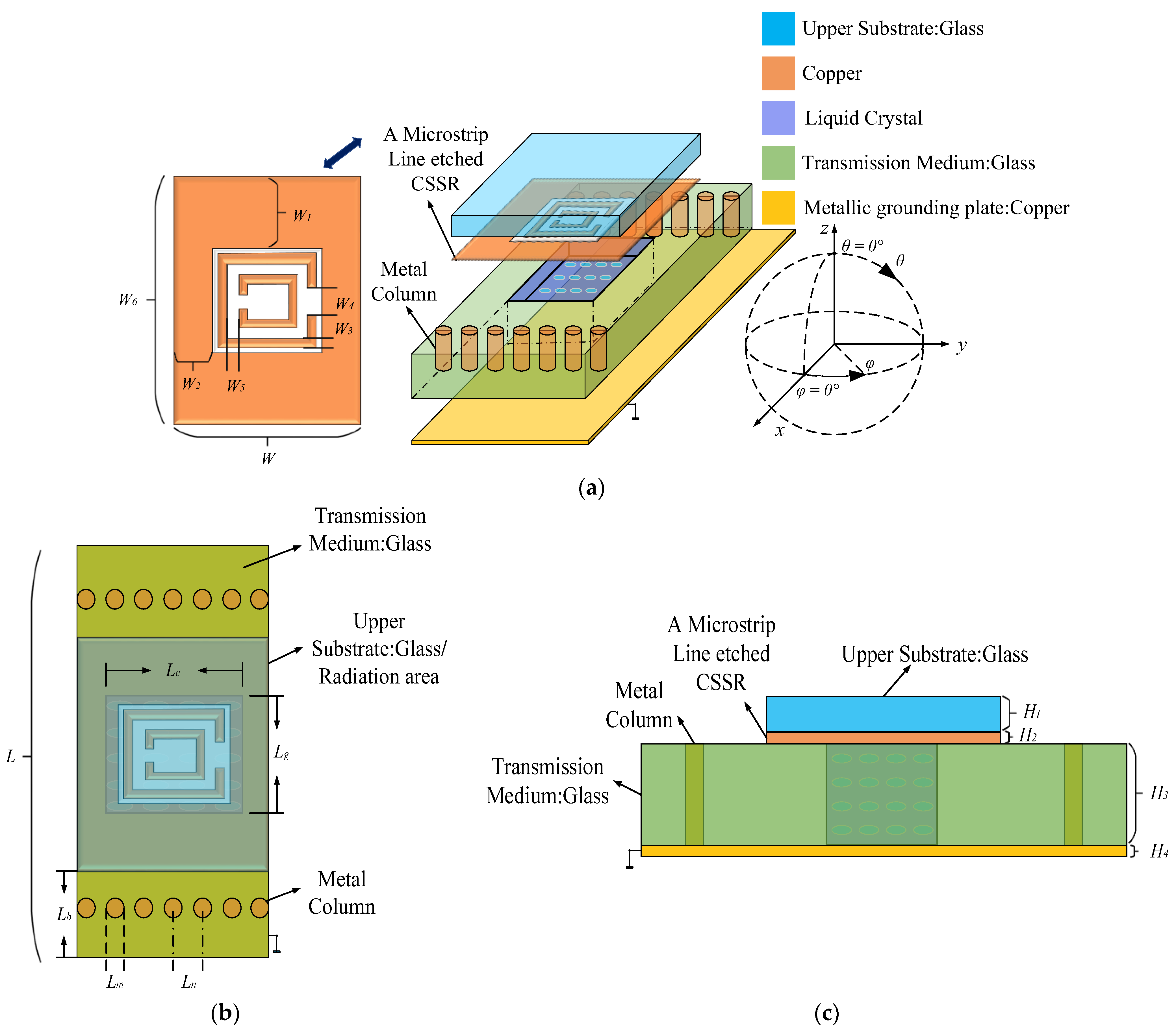
The leakage antenna designed in this paper utilizes an ML transmission structure. The ML transmission structure has the advantages of low cost, easy integration, and high flexibility, but the attenuation loss (such as dielectric loss, conductor loss, and scattering loss) is large. Recently, the substrate-integrated waveguide (SIW) transmission structure has been popularized for low energy loss. It connects the upper and lower layers of metal by placing two rows of metal columns in the substrate to realize electromagnetic wave transmission [8,58,59]. However, this structure has the disadvantages of a complicated fabrication process and poor flexibility in unit configuration. To combine the advantages of the two structures, we propose a metal-column embedded microstrip line (MCML) transmission structure based on the traditional ML structure by borrowing the structural characteristics, i.e., by placing two rows of metal posts in the SIW [45]. It is worth noting that, unlike SIW, the metal columns of the MCML structure do not play the role of connecting the upper and lower metal layers. Rather, they have two main roles: (1) limiting the electromagnetic wave propagation region, so that the electromagnetic wave is concentrated in the radiation region, thereby transmitting the electromagnetic wave more efficiently and decreasing the dissipation of energy, thus reducing the radiation loss; and (2) reducing the attenuation loss and improving the efficiency of energy radiation.
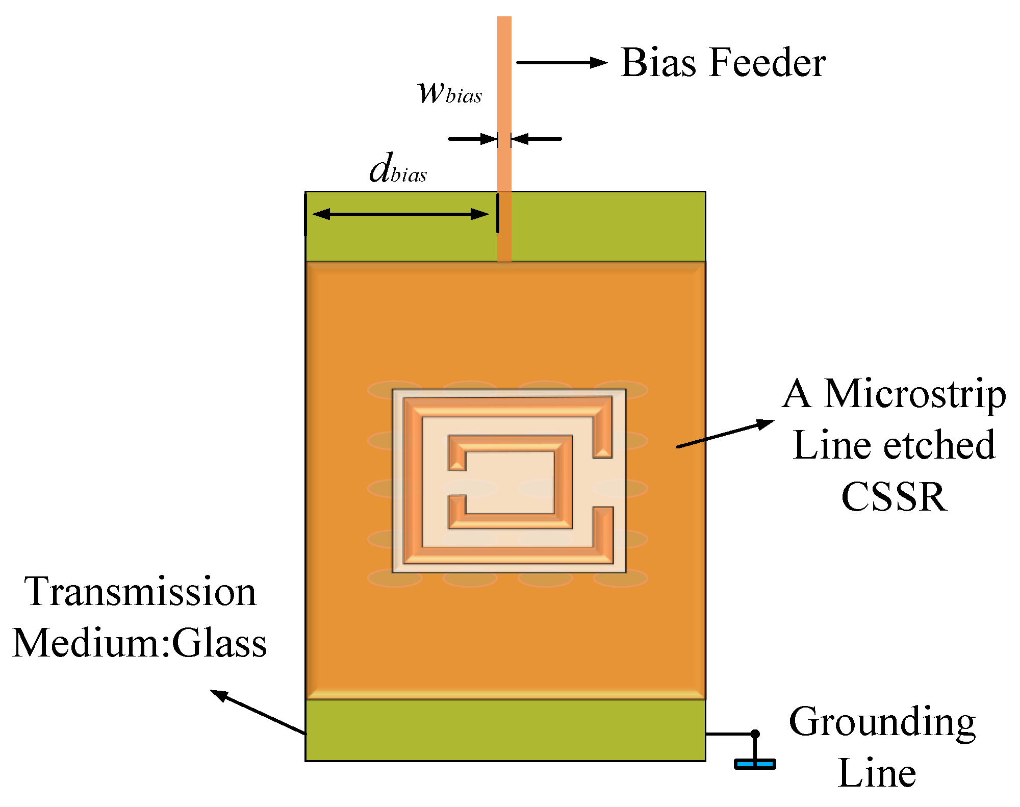
Figure 1 depicts the leakage antenna unit comprising a copper ground floor, a dielectric substrate, an ML etched with the CSRR structure, and an LC layer. The dielectric substrate consists of a 1.5-mm-thick glass with a relative dielectric constant of 5.5. A 0.035-mm-thick copper plate is placed at the bottom of the dielectric substrate as the ground floor. The ML etched the CSRR is made of metallic copper with a thickness of 2 μm and is topped with a 0.2 mm-thick glass layer. The LC layer is encapsulated in a dielectric substrate and filled between the ML and the ground metal plate. By introducing a bias voltage to form a pressure difference between the ML and the metal plate, the direction of the LC layer molecules can be controlled to change the antenna resonant frequency. Two rows of metal columns are placed on a dielectric substrate for a more efficient transmission of electromagnetic waves. The detailed dimensions of the antenna structure are shown in Table 2.
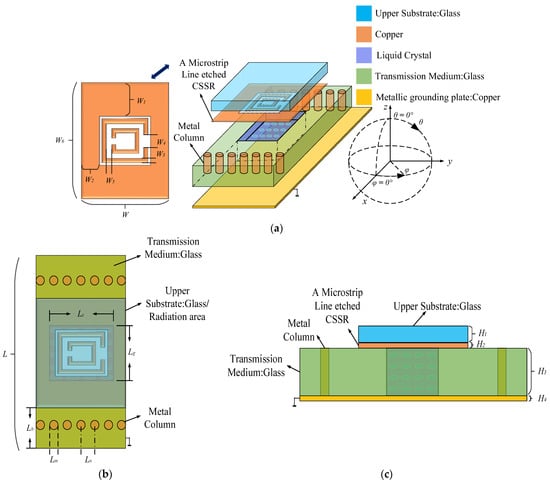
Figure 1.
The antenna cell structure. (a) Main view; (b) Top view; (c) left view.
Table 2.
Antenna cell parameters.
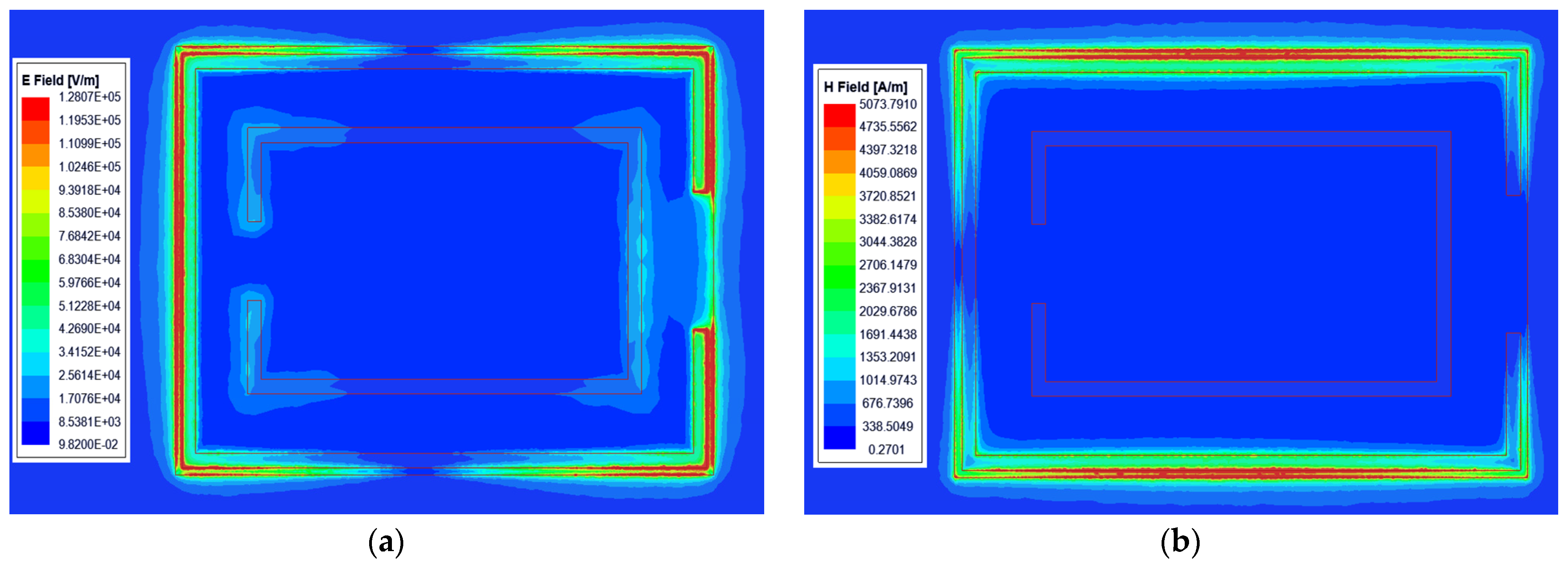
The Complementary Split Ring Resonator (CSRR) is a complementary form of the Split Ring Resonator (SRR) [60]. The SRR comprises two metal rings with identical centers and back-to-back openings and has negative magnetic permeability characteristics similar to those observed in CSRR. When excited by an axial magnetic field, the CSRR can be regarded as a magnetic dipole. At the same resonant frequency, the CSRR composed of multiple metal rings with the same center of the circle is compact compared to that composed of a single metal ring, rendering the device more miniaturized [61]. The electric and magnetic fields at the CSRR-shaped gap on the microstrip line are shown in Figure 2. The E field intensity is greatest at the open resonant ring of the CSRR slot (Figure 2a). This time-varying e-field can be expressed as a capacitance by the extended Ampere law. At the same time, the magnetic field is mainly distributed in the upper and lower sides of the outer ring of the gap (Figure 2b), which can be expressed as inductance by Faraday’s induction law. Therefore, CSRR gaps can be modelled with inductance (L), radiation resistance (R), and capacitance (C). By changing the geometrical parameters of the gap, L, R, and C will change, and the resonant frequency and coupling strength will also change.
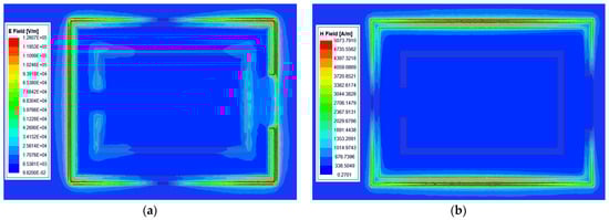
Figure 2.
Electric and magnetic field energy distribution at the CSRR slot. (a) Electric field energy distribution; (b) Magnetic field energy distribution.
The RF energy input to the antenna unit is set to Pin, the energy radiated from the CSRR slit to Prad, the dielectric loss to Pdie, the scattering loss to Psca, and the conductor loss to Pcon. Pdie, Psca, and Pcon are collectively referred to as the unwanted attenuation loss, denoted by Patt. S11 represents the reflection coefficient of the antenna, and S21 denotes the transmission coefficient. The radiation efficiency of the antenna can be expressed as:
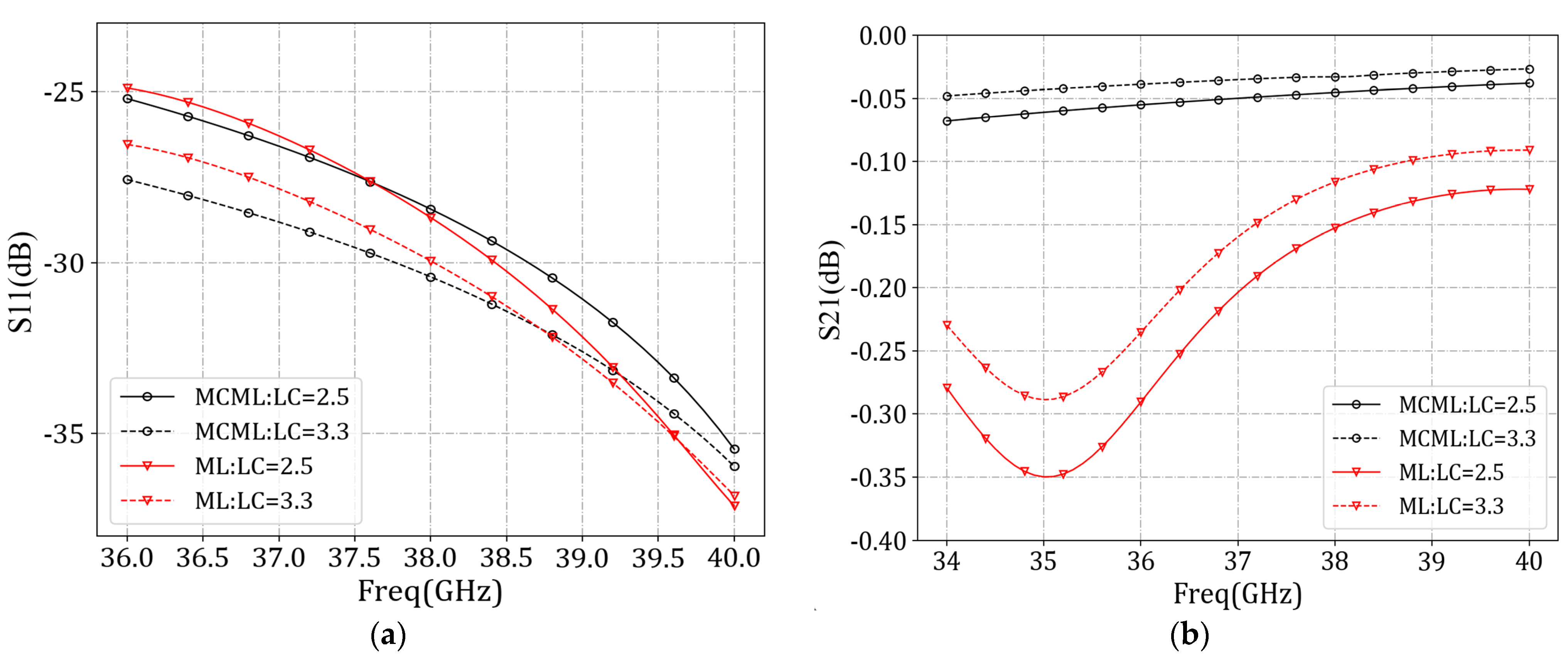
To verify the advantages of the MCML transmission structure, we removed the CSRR slot of the ML in the antenna structure to avoid the energy leakage from the microstrip line to free space, i.e., Prad was approximated to be 0. At the same time, the antenna element of the ML structure was used as a contrast structure. The difference between the two structures was that the MCML structure had two rows of metal columns. We used HFSS simulation software (Version 2020R1) to simulate and obtain the S11 (Figure 3a) and S21 (Figure 3b) comparison diagrams of the two structures. According to Figure 3a, there was very little difference in the S11 parameters between the two structures. At 38 GHz, the reflection coefficient of the MCML structure was smaller, indicating that the impedance-matching performance of the MCML structure was better at this frequency. From Figure 3b, it can be concluded that the change of LC dielectric constant had little effect on the transmission coefficient (S21), and the S21 parameters of the MCML structure was much higher than that of the ML structure in the whole frequency range of 35–45 GHz. According to Equation (8), Prad is approximated to be 0. The Pin of two structures was the same, the difference of S11 was negative, and the S21 parameters of the MCML were much higher than those of the ML, which indicated that the attenuation loss Patt of the ML structure was larger. Meanwhile, the MCML structure could reduce the useless attenuation of electromagnetic waves and improve energy utilization efficiency.
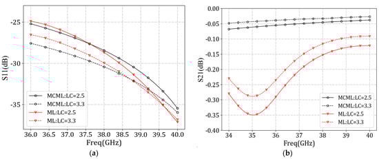
Figure 3.
Comparison of MCML and ML performance after removing the CSRR slot. (a) S11 parameters; (b) S21 parameters.
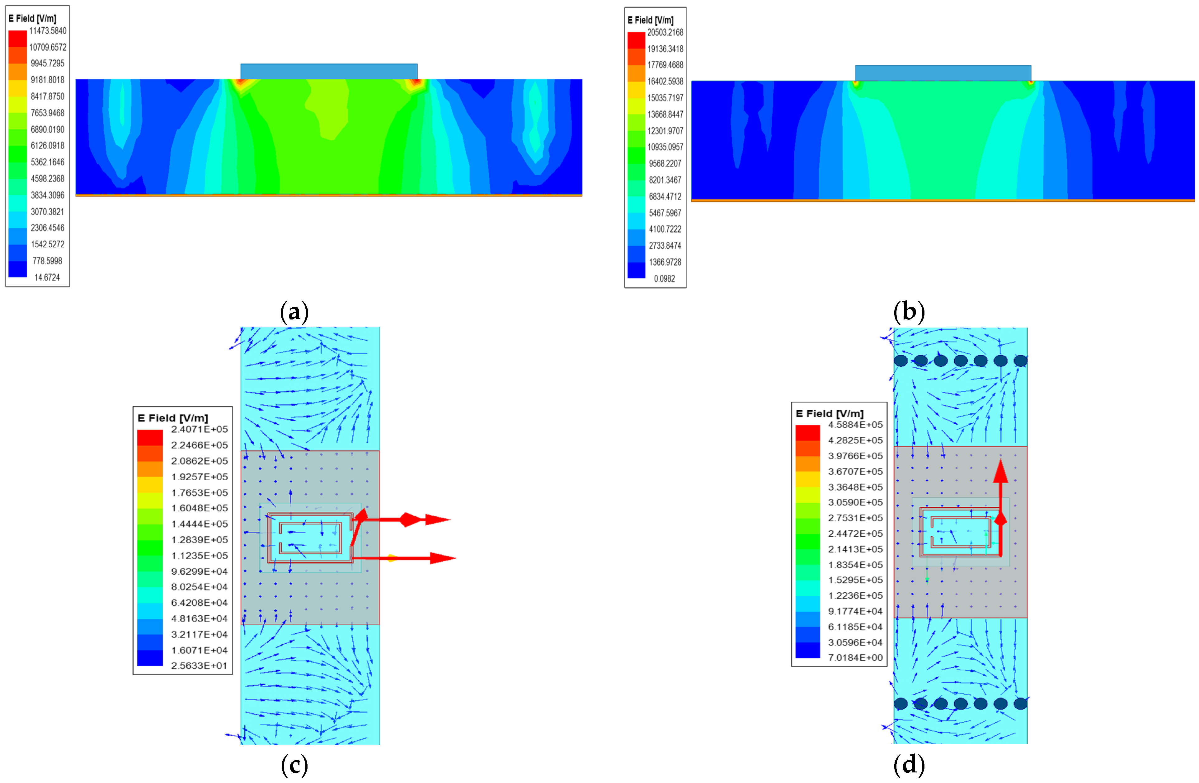
The interaction between the metal columns and the transmission medium in MCML structures can increase the energy coupling effect. By reasonably designing the shape and position of the metal columns, the propagation path of electromagnetic waves can be controlled, allowing energy to be more concentrated and transmitted to the target area, reducing beam diffusion. Figure 4a–d represent the electric field energy maps of ML and MCML at the output wave port, as well as the electric field vector maps of the antenna surface, respectively. Figure 4b shows that the MCML structure can concentrate electromagnetic wave energy more in the middle radiation region, reduce the beam diffusion degree, and increase the electric field energy value. Figure 4d shows more intuitively that the MCML structure can better control the transmission of electromagnetic waves, resulting in higher peak values of the electric field vector.
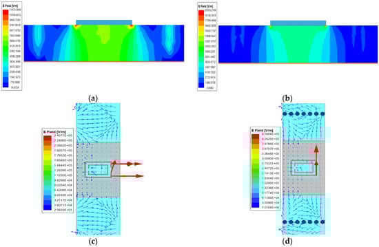
Figure 4.
Comparison of electromagnetic wave transmission between MCML and ML structures. (a) ML electric field energy map; (b) MCML electric field energy map; (c) ML electric field vector map; (d) MCML electric field vector map.
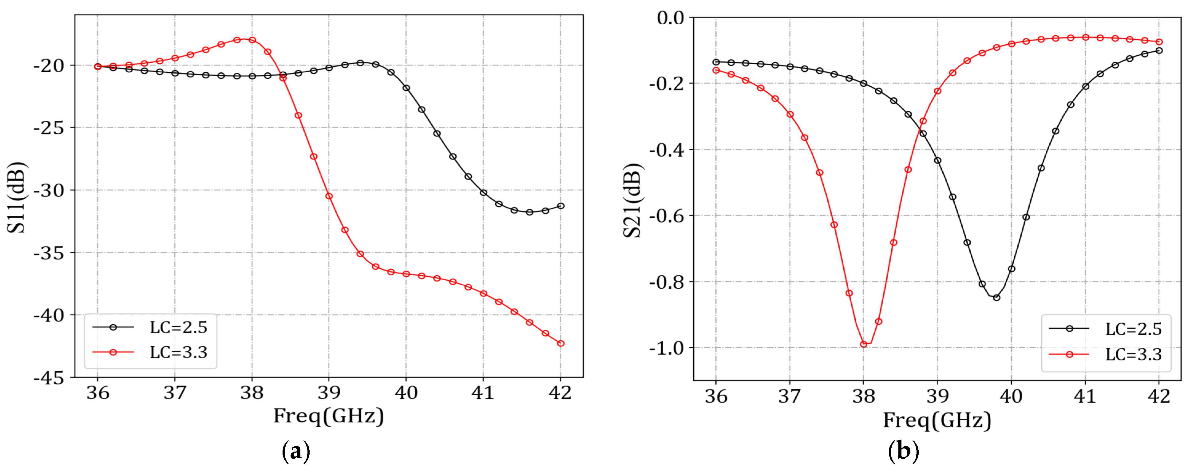
A simulation of the MCML structure yielded the S11 parameters (Figure 5a) and S21 parameters (Figure 5b). The antenna design employed GT3-23001 LC material. Altering the voltage applied to the upper and lower surfaces of the LC material induces a change in its dielectric constant from 2.5 to 3.3. This variation in dielectric constant leads to a shift in the resonant frequency of the resonator, subsequently impacting the energy coupled out from the slots and the radiation efficiency.
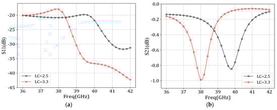
Figure 5.
MCML cell performance simulation. (a) S11 parameters; (b) S21 parameters.
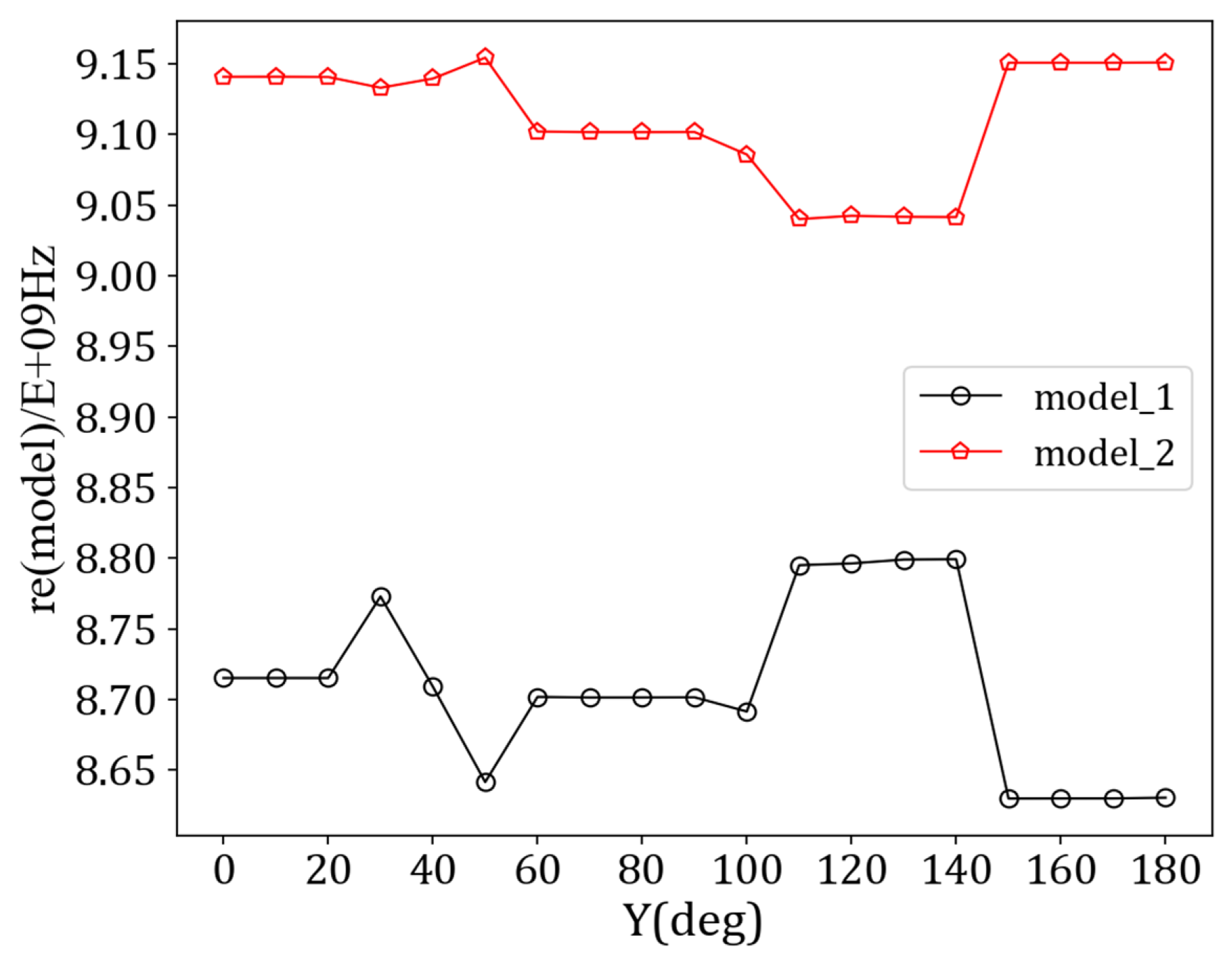
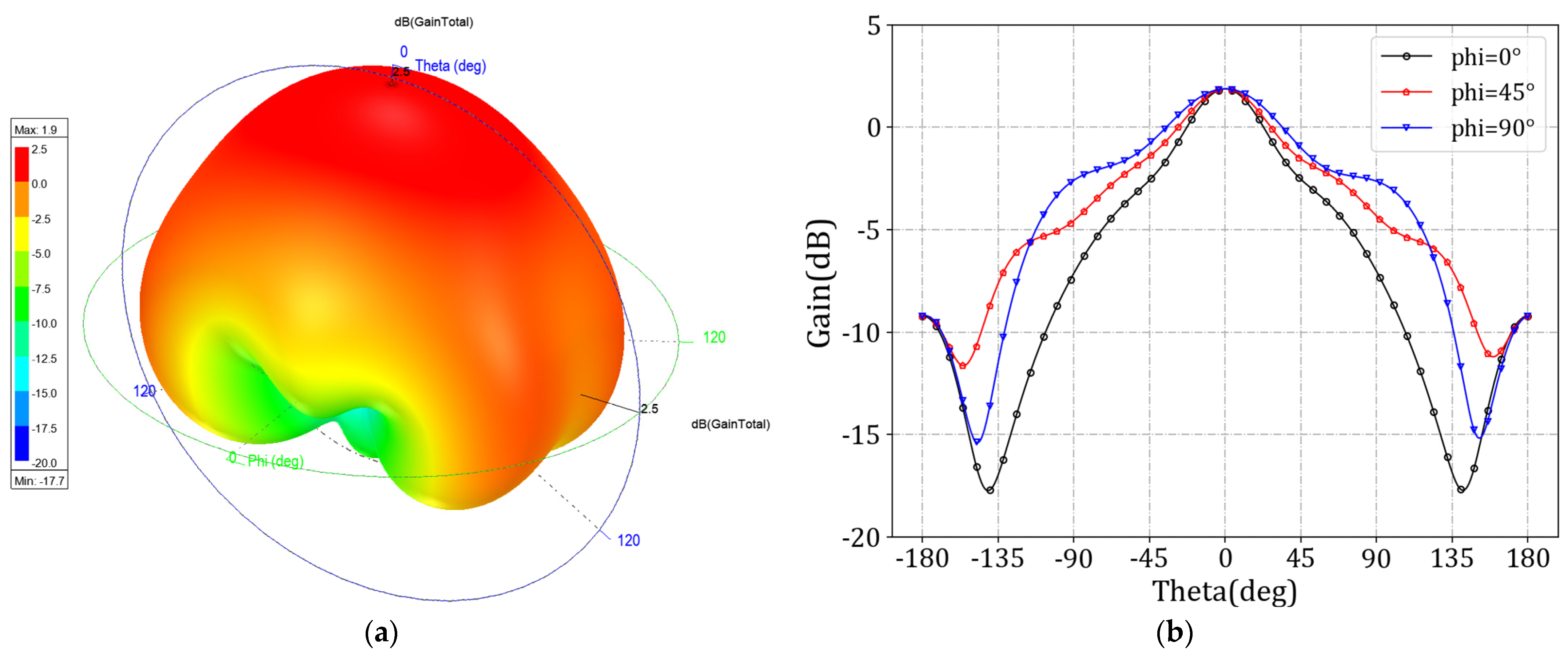
When the dielectric constant of the LC is 2.5, the antenna exhibits significant resonance characteristics at 38 GHz. The S11 parameters corresponding to this frequency are below −20 dB, indicating that the antenna unit has excellent impedance-matching performance. Figure 6 shows the dispersion curves of the antenna unit in both modes. The leaky-wave antenna designed in this paper is arranged periodically along the Y-axis direction, so the master–slave boundary condition is set in the Y direction. The angle parameter is taken from 0° to 180° in steps of 10°, and the dispersion curve is the result of a line scanning from 0°–180° parameter, with the vertical axis being the frequency. The three-dimensional far-field radiation diagram of the antenna is shown in Figure 7a. Due to the limited radiation energy of a single antenna unit, the antenna gain is low. Figure 7b shows the E-plane radiation map at different azimuth angles (phi), with slight changes in the E-plane radiation map as the azimuth angle changes.

Figure 6.
Dispersion curve of antenna unit.

Figure 7.
Radiation diagrams of MCML cell. (a) 3D plot; (b) 2D plot.
3.2. Antenna Array
The design and optimization of a leakage antenna cell with an MCML structure was described in the previous Section 3.1. This device may be used for 1D array configuration (see Figure 7). The radiation emitted by this array into free space can be conceptualized as a periodic LWA.
The structure of the periodic leakage antenna undergoes periodic changes as a whole. Considering an infinitely long periodic leakage antenna, the electromagnetic waves propagate in the y direction. The period length of the antenna is denoted as d and the propagation constant as , and the attenuation constant is assumed to be 0, with only a phase difference, described as . If the electric field in the first period is represented by E(z), then the electric field at that same position in the subsequent period is represented by . Formula (9) represents the field distribution in the leakage structure.
where Ed(x,y,z) is a function of period length d, which can be expanded by Fourier series as:
Substituting Formula (10) into Formula (9), the expression for the electric field distribution is given in Formula (11).
In the above formula,
It can be observed from Formulas (11) and (12) that the electric field E(x,y,z) is comprised of multiple harmonics, each with corresponding propagation constant. These propagation constants are determined by the fundamental mode propagation constants and the period between elements.
In accordance with the radiation conditions of leakage antennas, for periodic leakage antennas to radiate in the region where z is greater than 0, wave number kzn must also be greater than 0. Otherwise, electromagnetic waves will rapidly decay along the z direction. The free space propagation constant is denoted as k0, and the relationship between wave number kzn and phase constant βn are obtained as shown in Formula (13).
The radiation condition under which harmonics can be obtained is:
The fundamental mode of a periodic leakage antenna is typically a slow wave, with the propagation constant of the fundamental mode being βy > k0. The radiation condition for the n harmonics can be derived from Formula (14).
Formula (15) indicates that d becomes negative when n is greater than 0, which is not practical. When n is less than 0, the antenna can generate radiation for n harmonics by appropriately designing the period d. In this case, the value of βn can be greater than 0, equal to 0, or less than 0. Therefore, the periodic leakage antenna exhibits zero-cross-scanning characteristics.
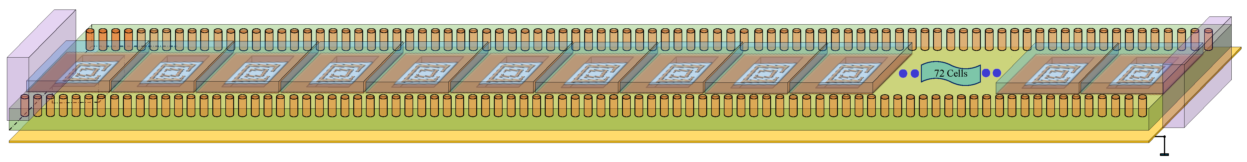
Arranging the 72 antenna units in one dimension, according to the principle of periodic leakage antennas, the choice of unit spacing greatly influences the antenna’s radiation characteristics. Take, for example, n = −1, so that the antenna array can generate −1 harmonic radiation. After optimizing the design, the spacing between units is 2 mm, and the antenna length is 123 mm, as shown in Figure 8.
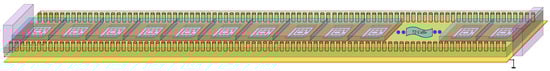
Figure 8.
Structure of the periodic leakage antenna array.
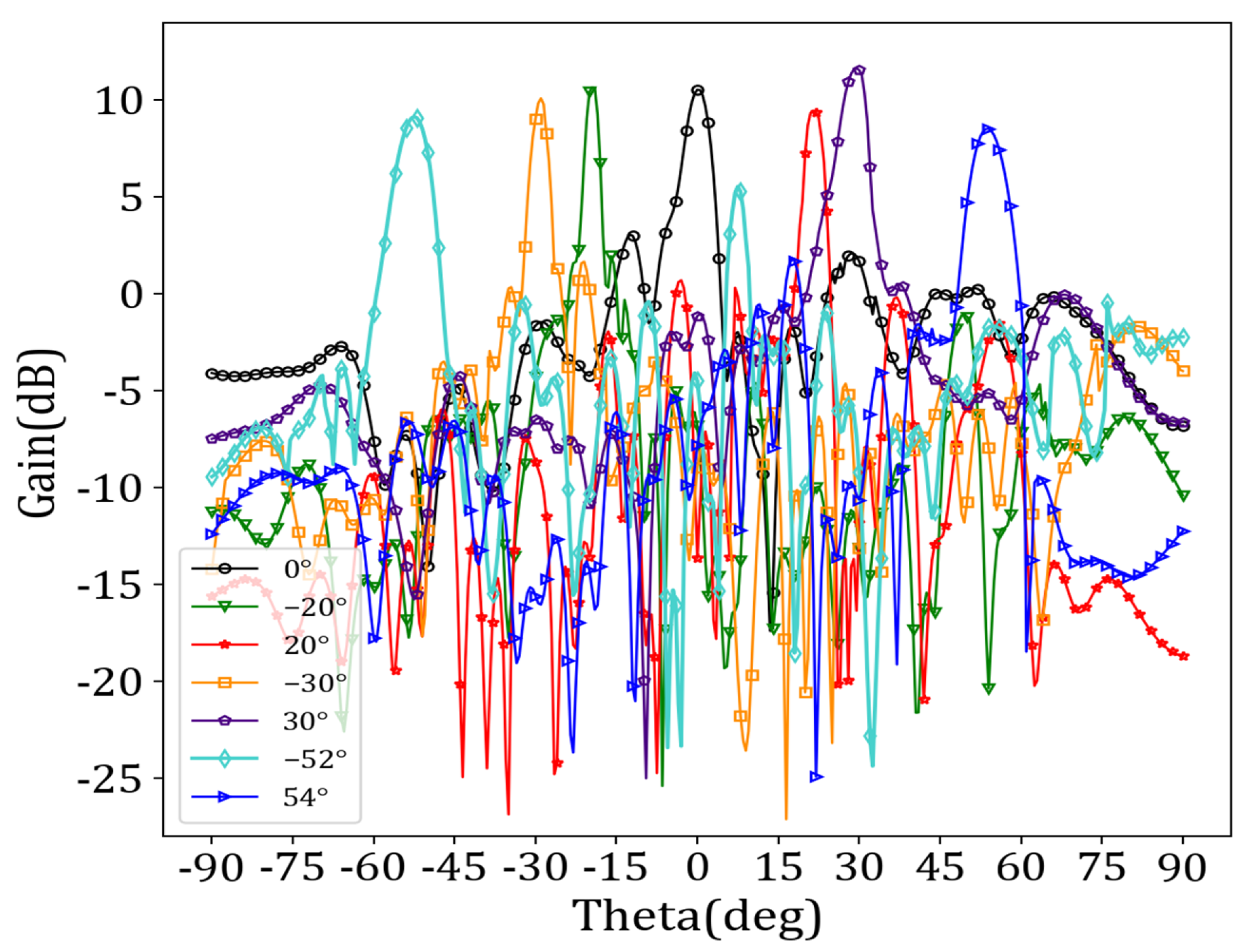
We set the operating frequency to 38 GHz and simulated the antenna performance using HFSS. The preset angles for beam scanning were −55°, −30°, −20°, 0°, 20°, 30°, and 60°, respectively. Table 3 displays the antenna unit‘s encoding sequence “0/1”, corresponding to each beam direction. The relative dielectric constant of the LC corresponding to “0” was 3.3, and the relative dielectric constant of the LC corresponding to “1” was 2.5. Figure 9 illustrates the radiation spatial beam gain maps corresponding to different beam directions.
Table 3.
Binary discrete amplitude-weighted sequences of 72 cells with different beam directions.
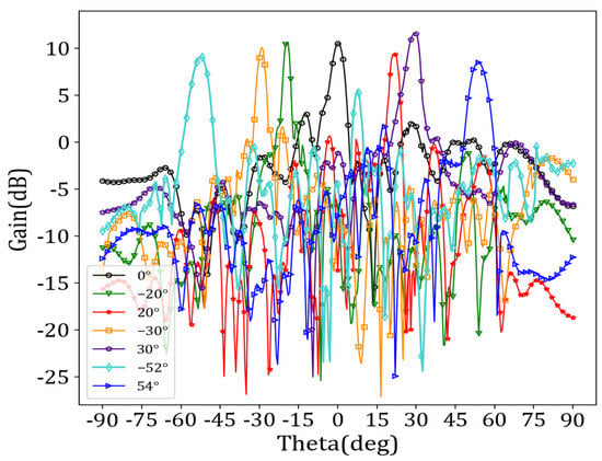
Figure 9.
Beam gain maps corresponding to different beam directions.
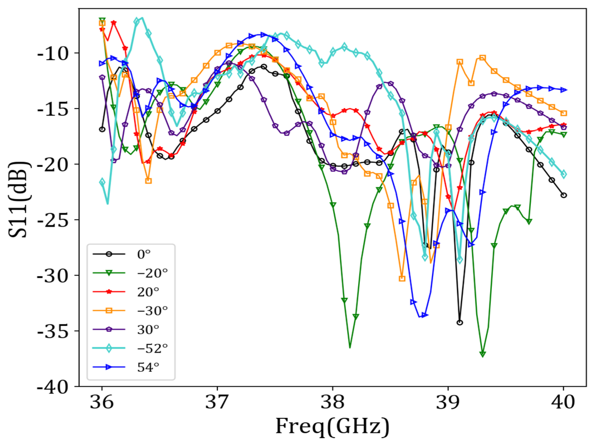
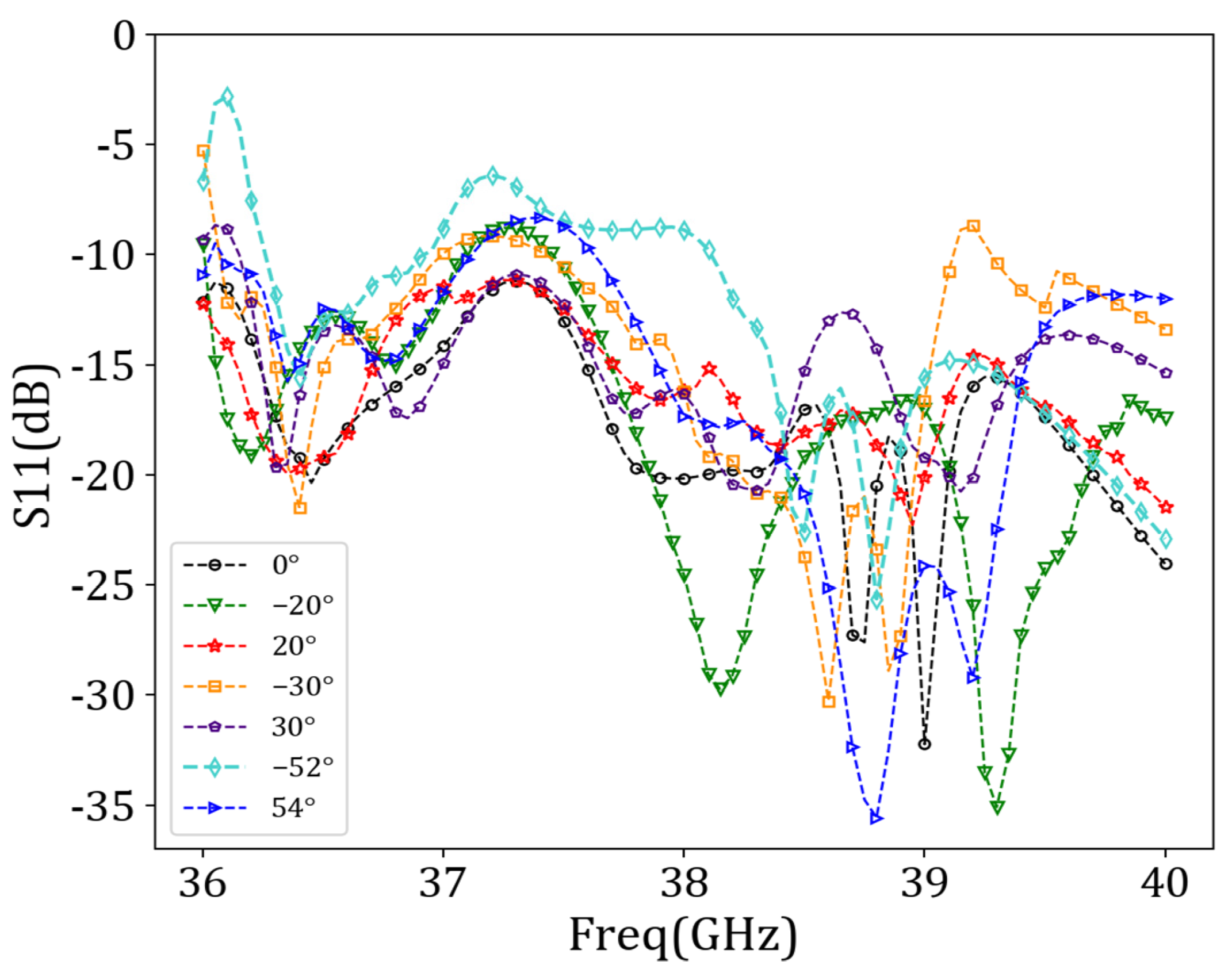
Figure 10 shows that the reflection coefficient (i.e., the S11 parameters) was essentially below −10 dB in the 36 GHz–40 GHz frequency range over a beam sweep from −52° to 54°, indicating an excellent impedance match.
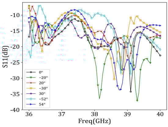
Figure 10.
Reflection coefficients corresponding to different beam directions.
As shown in Figure 9, the different beam directions aligned with expectations and exhibited a gain above 10 dB overall. Particularly at an angle of 30°, there was an angle deviation of just 0.4°, and a gain reaching as high as 11.65 dB could be achieved. Simulation experiments showed that the angle scanning range of the antenna could not reach −55° and 60°, and the angle scanning between −52° and 54° could be realized when working at 38 GHz. Table 4 shows specific angle deviations and main beam gains for different directions.
Table 4.
Angle deviations and gains corresponding to different beam directions.
3.3. Bias Feeder Design and Comparative Experiments
During the antenna testing, it was necessary to apply appropriate bias voltages between the metal ground plate and the ML to control the dielectric constant of the LC at each unit. This required loading a suitable bias feeder onto the antenna. However, introducing bias feeders to the antenna unavoidably affects its radiation characteristics to some extent. Hence, this section primarily investigates how to load the bias feeder onto the antenna structure and the actual impact on the antenna after loading the bias feeder.
The design of bias feeders mainly involves two aspects: the position of the loading of the bias feeder and the structure of the bias feeder. Firstly, it is necessary to determine the position of the bias feeder by applying bias voltage on the ML to control the variation of the LC dielectric constant. Since electromagnetic waves primarily radiate into free space through the CSRR slot on the ML, determining the position of the bias feeder on the ML is particularly important. As shown in Figure 2, the radiated energy mainly distributes around the open resonant rings of the CSRR structure. Therefore, it is not advisable to use the long side of the ML as the feeding point for the bias feeder, as this would significantly impact the radiation characteristics. Thus, the bias feeding point was placed on the short side of the ML, as illustrated in Figure 11. The width of the bias feeder was set to wbias, and the distance from the long side of the rectangular patch was set to dbias. We next determined the position that minimally affected the antenna’s radiation characteristics by simulating and analyzing different lengths of dbias values and wbias values.
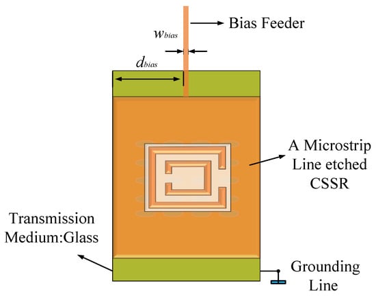
Figure 11.
Bias feeder structure.
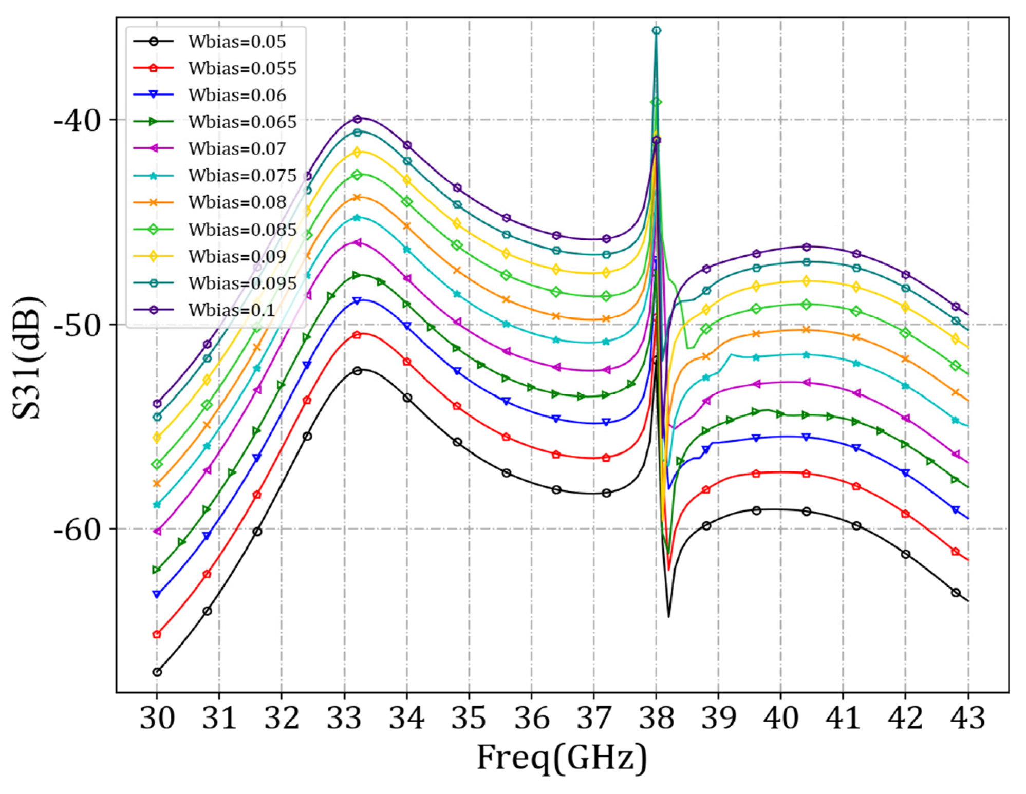
We first set dbias at 1 mm and set wbias values at 0.05 mm, 0.055 mm, 0.06 mm, 0.065 mm, 0.07 mm, 0.075 mm, 0.08 mm, 0.085 mm, 0.09 mm, 0.095 mm, and 0.1 mm, respectively, for simulation of the antenna unit. By scanning the values of wbias, the minimum S31 curve was identified in the simulation results. A smaller S31 value indicates a more minor influence between the bias feed voltage and the RF source, resulting in a lesser impact on the antenna radiation characteristics introduced by the bias feeder. Figure 12 demonstrates that as the width of the bias feeder decreased, the S31 parameters decreased, indicating a lesser influence between the bias feed voltage and the RF source. However, considering practicality, excessively narrow wbias values would pose challenges in processing and storage. Therefore, a value of 0.07 mm was applied.
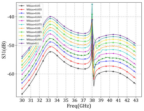
Figure 12.
Comparison curves of S31 parameters under different wbias values.
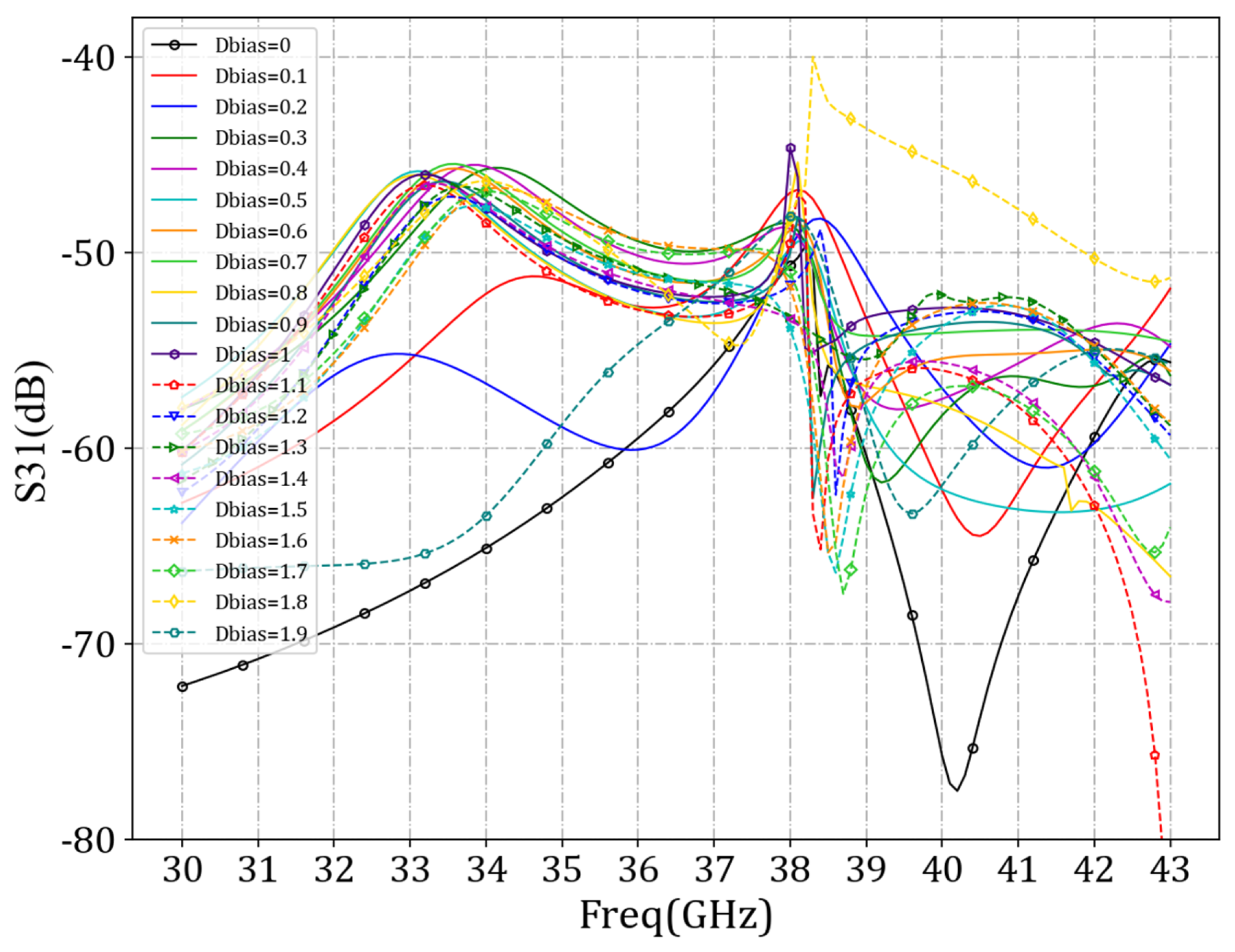
We next set wbias at 0.07 mm and dbias values at 0 mm, 0.1 mm, 0.2 mm, 0.3 mm, 0.4 mm, 0.5 mm, 0.6 mm, 0.7 mm, 0.8 mm, 0.9 mm, 1 mm, 1.1 mm, 1.2 mm, 1.3 mm, 1.4 mm, 1.5 mm, 1.6 mm, 1.7 mm, 1.8 mm, and 1.9 mm, respectively, for our simulation of the antenna unit. By scanning the values of dbias, the minimum S31 parameter value was found in the simulation results. As shown in Figure 13, when dbias was set to 1.5 mm, the S31 parameter value was minimized at 38 GHz.
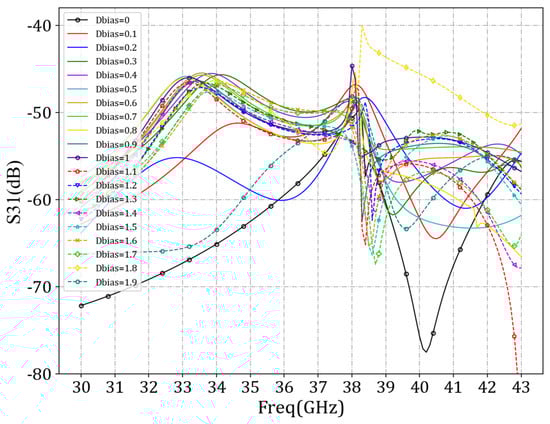
Figure 13.
Comparison curves of S31 parameters under different dbias values.
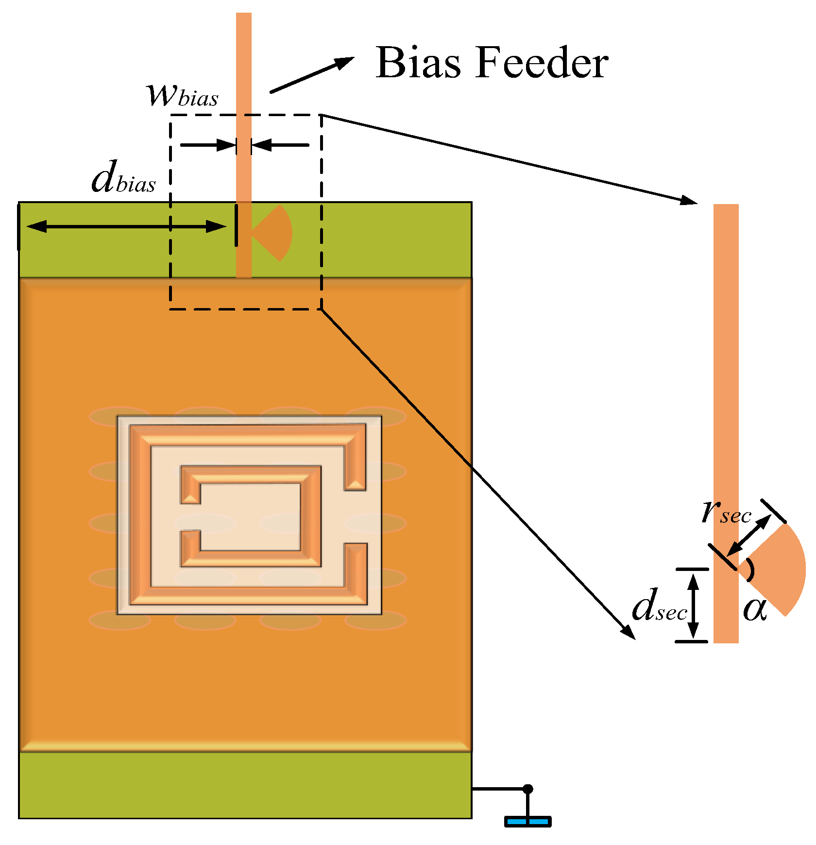
To further minimize the impact of RF signals on the DC source while avoiding the DC bias voltage becoming part of the RF circuit as much as possible, ensuring the stable operation of the antenna, it was necessary to place a blocking structure at the appropriate position of the bias feeder. Assuming the bias feeder as a transmission line, for RF signals, the end connecting to the ML served as the RF input port. According to transmission line principles, when the electrical length of the ML is λg/4 (where λg is the guided wavelength), the output end becomes short-circuited, and the input end exhibits a high impedance state. By placing a low impedance component at λg/4, it can be approximately considered that the transmission line is short-circuited at λg/4, blocking the RF signal from entering the bias feeder. We utilized a sector-shaped structure to achieve this blocking function. This sector-shaped patch can be equivalent to a low-impedance component. As shown in Figure 14, we placed the sector-shaped patch at a distance of λg/4 from the narrow edge of the ML, i.e., dsec = λg/4, with the radius rsec and an angle α of 90°.

Figure 14.
Sector-blocking bias feeder structure.
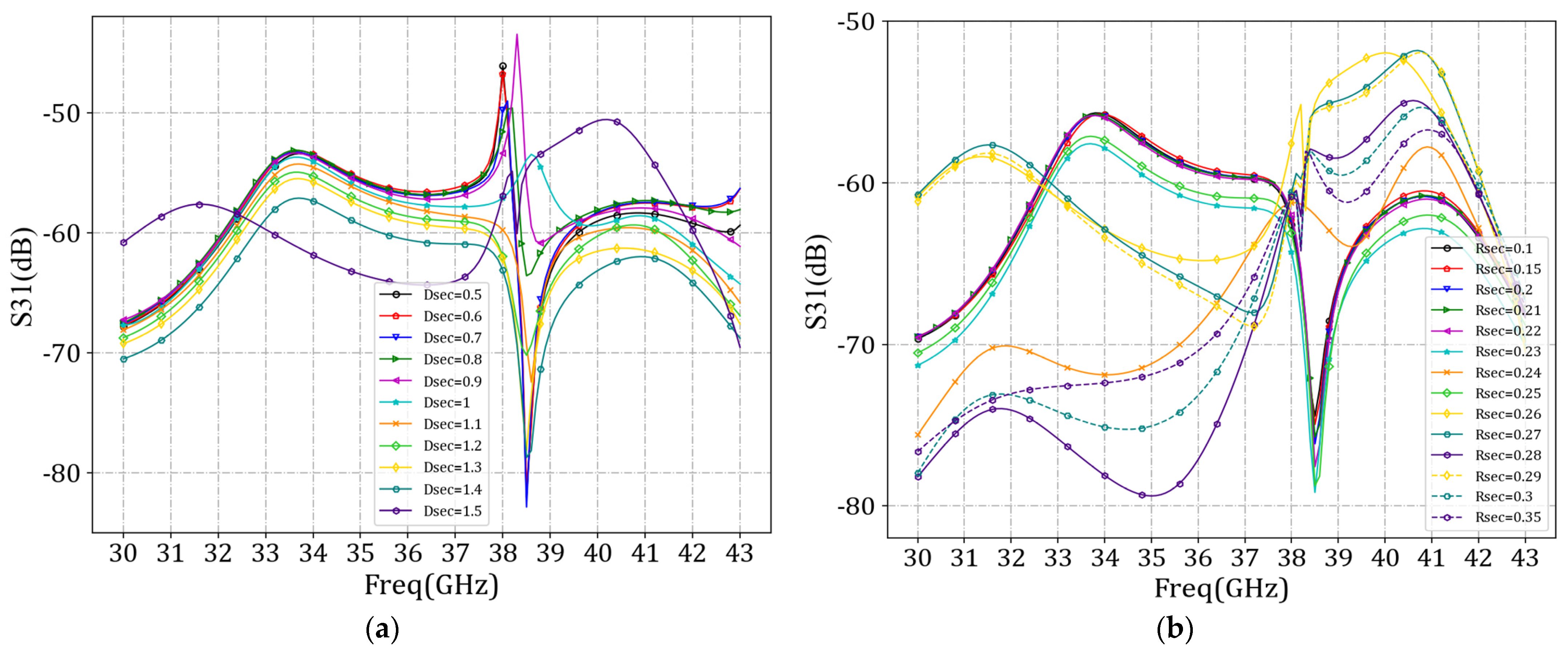
We then set dbias at 1.5 mm and determined the values of dsec and rsec. Due to the loading of the bias feeder, the actual value of the guided wavelength of the antenna unit could not be precisely calculated. The value of dsec had to be scanned to obtain the minimum S31 curve in the simulation results. Before scanning the value of dsec, it was necessary to determine the scanning range. Calculating the guided wavelength at 38 GHz without loading the bias feeder yielded a value of 3.6 mm. Therefore, the range of dsec was set from 0.5 mm to 1.5 mm, with a scanning interval of 0.1 mm. Initially, rsec was set to 0.25 mm. The scanning results are shown in Figure 15a. When the value of dsec was 1.4 mm, the S31 parameter was minimized at 38 GHz. With dsec fixed at 1.4 mm, we determined the value of rsec. The range of rsec was set from 0.1mm to 0.35 mm. The scanning results, as shown in Figure 15b, indicated that the S31 parameter was minimized at 38 GHz when the value of rsec was 0.23 mm.
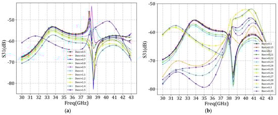
Figure 15.
Comparison curves of S31 parameters under different dsec and rsec values. (a) dsec; (b) rsec.
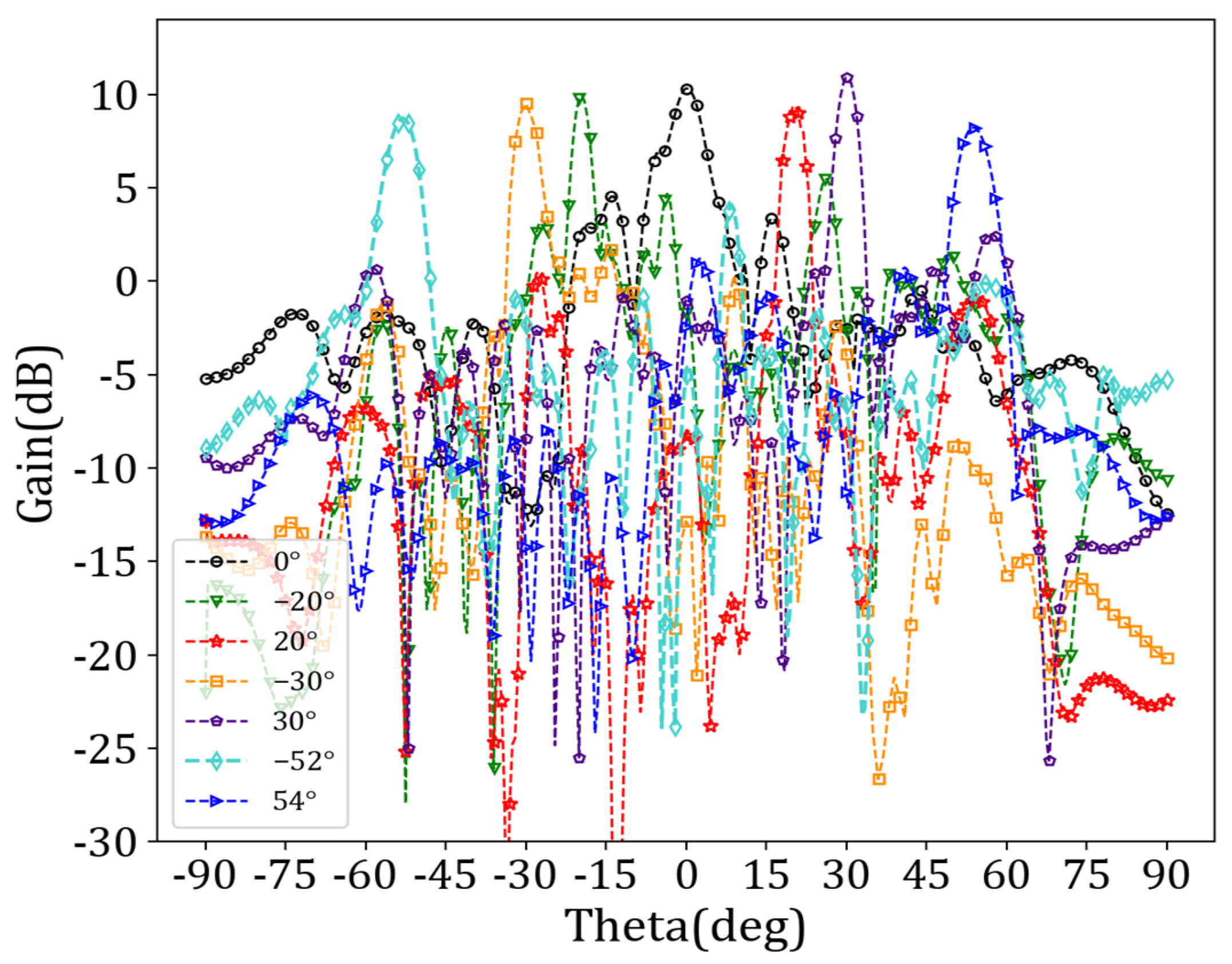
Finally, we set wbias to 0.07 mm and dbias to 1.5 mm, dsec to 1.4 mm, and rsec to 0.23 mm. After determining the position and structure of the bias feeder, the antenna cell with the bias feeder was assembled into an array, and the overall structure of the antenna was simulated to analyze the impact of the bias network on antenna radiation. Preset angles were set to −55°, −30°, 0°, 30°, and 60°. We employed the binary beam control method to reconstruct the target beam. Figure 16 and Figure 17 show the beam scanning results and reflection coefficients, respectively.
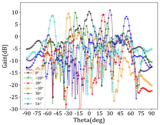
Figure 16.
Beam gain diagrams corresponding to different beam directions after adding bias feeder.
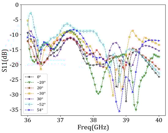
Figure 17.
Reflection coefficients corresponding to different beam directions after adding bias feeder.
Figure 16 indicates that the angle scanning range of the antenna array remained within the range of −52° to 54° after adding the bias feeder network. However, there was a slight deviation in the specific angle scanning range, from −51.7° to 53.8°. The impedance-matching performance was satisfactory. Table 5 provides particular angle deviations and main beam gains for different beam directions.
Table 5.
The angle deviations and gains corresponding to different beam directions.
Table 5 provides the specific beam scanning range and each angle’s gain. Compared to the antenna gain values presented in Table 4, there was a certain degree of decrease in the actual gain at each angle, with the maximum decrease being 0.758 dB and an average reduction of 0.451 dB. Overall, the impact on the antenna radiation performance after adding bias feeders was minimal, which is crucial for practical engineering applications.
4. Conclusions
This paper presents a fixed-frequency beam scanning leakage antenna based on LC. The antenna used 72 CSRRs arranged periodically to achieve beam scanning. The LC layer was encapsulated in the transmission medium between the ML and the metal ground floor. By adding a bias voltage to the ML, the voltage difference between the upper and lower surfaces of the LC layer could be formed to realize the feeding of the LC layer. Combined with the holographic principle, the antenna could achieve continuous beam scanning at 38 GHz from −52° to 54°. We designed the sector-blocking bias feeder structure to minimize the interaction between the introduced bias voltage and the RF source. The beam scanning performance of the antenna was re-simulated after the addition of the bias network. Experiments showed that the bias feeder’s effect on the antenna radiation performance was tiny.
Author Contributions
Conceptualization, S.H.; methodology, S.H.; software, S.H.; validation, Y.L.; formal analysis, Z.M.; resources, S.F.; data curation, J.L.; writing-original draft preparation, S.H.; writing-review and editing, S.H.; supervision, Y.F.; funding acquisition, S.F. All authors have read and agreed to the published version of the manuscript.
Funding
This research is funded by Key Basic Research Projects of the Basic Strengthening Program, grant number 2020-JCJQ-ZD-071.
Institutional Review Board Statement
Not applicable.
Informed Consent Statement
Not applicable.
Data Availability Statement
Data are contained within the article.
Conflicts of Interest
The authors declare no conflict of interest.
References
- Shen, F.; Hu, Q.; Gong, C. Determining the Antenna Phase Center for the High-Precision Positioning of Smartphones. Sensors 2024, 24, 2243. [Google Scholar] [CrossRef] [PubMed]
- Wei, D.; Zhang, P. A Linearly and Circularly Polarization-Reconfigurable Leaky Wave Antenna Based on SSPPs-HSIW. Electronics 2023, 12, 2602. [Google Scholar] [CrossRef]
- Menzione, F.; Paonni, M. 3D Galileo Reference Antenna Pattern for Space Service Volume Applications. Sensors 2024, 24, 2220. [Google Scholar] [CrossRef] [PubMed]
- Al-Gburi, A.J.A.; Zakaria, Z.; Alsariera, H.; Akbar, M.F.; Ibrahim, I.M.; Ahmad, K.S.; Al-Bawri, S.S. Broadband circular polarised printed antennas for indoor wireless communication systems: A comprehensive review. Micromachines 2022, 13, 1048. [Google Scholar] [CrossRef] [PubMed]
- Ushikoshi, D.; Higashiura, R.; Tachi, K.; Fathnan, A.A.; Mahmood, S.; Takeshita, H.; Wakatsuchi, H. Pulse-driven self-reconfigurable meta-antennas. Nat. Commun. 2023, 14, 633. [Google Scholar] [CrossRef] [PubMed]
- Munoz-Martin, J.F.; Onrubia, R.; Pascual, D.; Park, H.; Camps, A.; Rüdiger, C.; Monerris, A. Untangling the incoherent and coherent scattering components in GNSS-R and novel applications. Remote Sens. 2020, 12, 1208. [Google Scholar] [CrossRef]
- Xu, F.; Wu, K.; Zhang, X. Periodic leaky-wave antenna for millimeter wave applications based on substrate integrated waveguide. IEEE Trans. Antennas Propag. 2009, 58, 340–347. [Google Scholar]
- Liu, J.; Jackson, D.R.; Long, Y. Substrate integrated waveguide (SIW) leaky-wave antenna with transverse slots. IEEE Trans. Antennas Propag. 2011, 60, 20–29. [Google Scholar] [CrossRef]
- Morshed, K.M.; Karmokar, D.K.; Esselle, K.P.; Matekovits, L. Beam-Switching Antennas for 5G Millimeter-Wave Wireless Terminals. Sensors 2023, 23, 6285. [Google Scholar] [CrossRef]
- Hu, C.C.; Jou, C.F.; Wang, C.J.; Lee, S.H.; Wu, J.J. Coplanar waveguide to coplanar strips-fed active leaky-wave antenna. Microw. Opt. Technol. Lett. 1998, 19, 335–338. [Google Scholar] [CrossRef]
- Xiao, S.; Wang, B.Z.; Yang, X.S.; Wang, G. A novel reconfiguration CPW leaky-wave antenna for millimeter-wave application. Int. J. Infrared Millim. Waves 2002, 23, 1637–1648. [Google Scholar] [CrossRef]
- Ali, M.Z.; Khan, Q.U. High gain backward scanning substrate integrated waveguide leaky wave antenna. IEEE Trans. Antennas Propag. 2020, 69, 562–565. [Google Scholar] [CrossRef]
- Fu, Z.; Jiang, D.; Zhang, T.; Li, X. Ku-band liquid-crystal-based frequency reconfigurable comb siw slot leaky-wave antenna. In Proceedings of the 2018 International Conference on Microwave and Millimeter Wave Technology (ICMMT), Chengdu, China, 7–11 May 2018; pp. 1–3. [Google Scholar]
- Geng, Y.; Wang, J.; Li, Z.; Li, Y.; Chen, M.; Zhang, Z. Dual-beam and tri-band SIW leaky-wave antenna with wide beam scanning range including broadside direction. IEEE Access 2019, 7, 176361–176368. [Google Scholar] [CrossRef]
- Ranjan, R.; Ghosh, J. SIW-based leaky-wave antenna supporting wide range of beam scanning through broadside. IEEE Antennas Wirel. Propag. Lett. 2019, 18, 606–610. [Google Scholar] [CrossRef]
- Xu, J.; Hong, W.; Tang, H.; Kuai, Z.; Wu, K. Half-mode substrate integrated waveguide (HMSIW) leaky-wave antenna for millimeter-wave applications. IEEE Antennas Wirel. Propag. Lett. 2008, 7, 85–88. [Google Scholar]
- Cheng, Y.J.; Hong, W.; Wu, K.; Fan, Y. Millimeter-wave substrate integrated waveguide long slot leaky-wave antennas and two-dimensional multibeam applications. IEEE Trans. Antennas Propag. 2010, 59, 40–47. [Google Scholar] [CrossRef]
- Saghati, A.P.; Mirsalehi, M.M.; Neshati, M.H. A HMSIW circularly polarized leaky-wave antenna with backward, broadside, and forward radiation. IEEE Antennas Wirel. Propag. Lett. 2014, 13, 451–454. [Google Scholar] [CrossRef]
- Liu, C.Y.; Chu, Q.X.; Huang, J.Q. Double-side radiating leaky-wave antenna based on composite right/left-handed coplanar-waveguide. Prog. Electromagn. Res. Lett. 2010, 14, 11–19. [Google Scholar] [CrossRef]
- Cheng, Y.J.; Guo, Y.X.; Bao, X.Y.; Ng, K.B. Millimeter-wave low temperature co-fired ceramic leaky-wave antenna and array based on the substrate integrated image guide technology. IEEE Trans. Antennas Propag. 2013, 62, 669–676. [Google Scholar] [CrossRef]
- Malhat, H.A.; Elhenawy, A.S.; Zainud-Deen, S.H.; Al-Shalaby, N.A. Planar reconfigurable plasma leaky-wave antenna with electronic beam-scanning for MIMO applications. Wirel. Pers. Commun. 2023, 128, 1–18. [Google Scholar] [CrossRef]
- Cao, X.W.; Deng, C.J.; Kamal, S. Fixed-frequency beam steering leaky-wave antenna with integrated 2-bit phase shifters. IEEE Trans. Antennas Propag. 2022, 70, 11246–11251. [Google Scholar] [CrossRef]
- Du, H.; Wang, J.; Li, Z.; Zheng, W.; Zhang, L. A Broadband Fixed-Beam Leaky-Wave Antenna with Switchable Beam Direction. IEEE Antennas Wirel. Propag. Lett. 2023, 23, 169–173. [Google Scholar] [CrossRef]
- Zheng, W.; Wang, J.H.; Zhao, H.Y.; Zheng, L.; Geng, Y.J.; Li, Y.J.; Chen, M.; Zhan, Z. A leaky-wave antenna with capability of fixed frequency beamforming scanning. IEEE Trans. Antennas Propag. 2023, 71, 7585–7590. [Google Scholar] [CrossRef]
- Apaydin, N.; Sertel, K.; Volakis, J.L. Nonreciprocal and magnetically scanned leaky-wave antenna using coupled CRLH lines. IEEE Trans. Antennas Propag. 2014, 62, 2954–2961. [Google Scholar] [CrossRef]
- Esquius-Morote, M.; Gómez-Dı, J.S.; Perruisseau-Carrier, J. Sinusoidally modulated graphene leaky-wave antenna for electronic beamscanning at THz. IEEE Trans. Terahertz Sci. Technol. 2014, 4, 116–122. [Google Scholar] [CrossRef]
- Cheng, Y.; Wu, L.S.; Tang, M.; Zhang, Y.P.; Mao, J.F. A sinusoidally-modulated leaky-wave antenna with gapped graphene ribbons. IEEE Antennas Wirel. Propag. Lett. 2017, 16, 3000–3004. [Google Scholar] [CrossRef]
- Soleimani, H.; Homayoon, O. A novel 2D leaky wave antenna based on complementary graphene patch cell. J. Phys. D Appl. Phys. 2020, 53, 255301. [Google Scholar] [CrossRef]
- Al-Shalaby, N.A.; Elhenawy, A.S.; Zainud-Deen, S.H.; Malhat, H.A. Electronic beam-scanning strip-coded graphene leaky-wave antenna using single structure. Plasmonics 2021, 16, 1427–1438. [Google Scholar] [CrossRef]
- Fuscaldo, W.; Tofani, S.; Zografopoulos, D.C.; Baccarelli, P.; Burghignoli, P.; Beccherelli, R.; Galli, A. Tunable Fabry–Perot cavity THz antenna based on leaky-wave propagation in nematic liquid crystals. Antennas Wirel. Propag. Lett. 2017, 16, 2046–2049. [Google Scholar] [CrossRef]
- Martini, E.; Pavone, S.; Albani, M.; Maci, S.; Martorelli, V.; Giodanengo, G.; Ferraro, A.; Beccherelli, R.; Toso, G.; Vecchi, G. Reconfigurable antenna based on liquid crystals for continuous beam scanning with a single control. In Proceedings of the 2019 IEEE International Symposium on Antennas and Propagation and USNC-URSI Radio Science Meeting, Atlanta, GA, USA, 7–12 July 2019; pp. 449–450. [Google Scholar]
- Torabi, E.; Rozhkova, A.; Chen, P.-Y.; Erricolo, D. Compact and reconfigurable leaky wave antenna based on a tunable substrate integrated embedded metasurface. In Proceedings of the 2020 IEEE International Symposium on Antennas and Propagation and North American Radio Science Meeting, Toronto, ON, Canada, 5–10 July 2020; pp. 163–164. [Google Scholar]
- Fu, J.H.; Li, A.; Chen, W.; Lv, B.; Wang, Z.; Li, P.; Wu, Q. An electrically controlled CRLH-inspired circularly polarized leaky-wave antenna. IEEE Antennas Wirel. Propag. Lett. 2016, 16, 760–763. [Google Scholar] [CrossRef]
- Zvolensky, T.; Chicherin, D.; Räisänen, A.V.; Simovski, C. Leaky-wave antenna based on micro-electromechanical systems-loaded microstrip line. IET Microw. Antennas Propag. 2011, 5, 357–363. [Google Scholar] [CrossRef]
- Li, J.; He, M.; Wu, C.; Zhang, C. Radiation-pattern-reconfigurable graphene leaky-wave antenna at terahertz band based on dielectric grating structure. IEEE Antennas Wirel. Propag. Lett. 2017, 16, 1771–1775. [Google Scholar] [CrossRef]
- Damm, C.; Maasch, M.; Gonzalo, R.; Jakoby, R. Tunable composite right/left-handed leaky wave antenna based on a rectangular waveguide using liquid crystals. In Proceedings of the 2010 IEEE MTT-S International Microwave Symposium, Anaheim, CA, USA, 23–28 May 2010; pp. 13–16. [Google Scholar]
- Roig, M.; Maasch, M.; Damm, C.; Jakoby, R. Steerable Ka-Band leaky wave antenna based on liquid crystal material. In Proceedings of the 2013 7th International Congress on Advanced Electromagnetic Materials in Microwaves and Optics, Piscataway, NJ, USA, 16–21 September 2013; pp. 540–545. [Google Scholar]
- Liu, X.X. Study of Liquid Crystal Electronically Controlled Scanning Leaky-Wave Antennas. Ph.D. Thesis, Harbin Institute of Technology, Harbin, China, 2015; pp. 22–49. [Google Scholar]
- Gao, Y.; Lyu, Y.L.; Meng, F.Y.; Wu, Q. Electrically steerable leaky-wave antenna capable of both forward and backward radiation based on liquid crystal. Asia-Pac. Microw. Conf. (APMC) 2015, 2, 1–3. [Google Scholar]
- Liu, Y.L.; He, Z.Y.; Feng, W.; Li, K.; WANG, D.C. Design of Microstrip Leaky Wave Antenna Based on Liquid Crystal Material. Proc. Natl. Microw. Millim. Wave Conf. 2017, 2, 49–52. [Google Scholar]
- Gao, F. Reconfigurable Holographic Metamaterial Antenna Research. Master’s Thesis, Nanjing University of Aeronautics and Astronautics, Nanjing, China, 2018. [Google Scholar]
- Wang, Z.; Fu, Z.H.; Wu, T.H.; Jiang, D. Beam-scanning leaky-wave antennas based on liquid crystal materials. In Proceedings of the 2019 Annual National Conference on Antennas, Atlanta, GA, USA, 16–18 October 2019; pp. 292–294. [Google Scholar]
- Liu, Q. Study of Liquid Crystal-Based Beam-Scanning Holographic Hypersurface Leaky-Wave Antennas. Master’s Thesis, University of Electronic Science and Technology of China, Chengdu, China, 2020. [Google Scholar]
- Zhang, W.; Yang, W.; Jiang, D.; Hu, W.; Pan, P. Design of mm-wave Reconfigurable holographic antenna based on liquid crystal material. In Proceedings of the 2022 IEEE Conference on Antenna Measurements and Applications (CAMA), Guangzhou, China, 14–17 November 2022; pp. 1–5. [Google Scholar]
- Hou, S.; Fang, S.; Wang, Y.; Wang, M.; Wang, Y.; Tian, J.; Feng, J. A Ka-band one-dimensional beam scanning leaky-wave antenna based on liquid crystal. Sci. Rep. 2024, 14, 3937. [Google Scholar] [CrossRef] [PubMed]
- Deo, P.; Mirshekar-Syahkal, D. 60 GHz beam-steering slotted patch antenna array using liquid crystal phaseshifters. In Proceedings of the 2012 IEEE International Symposium on Antennas and Propagation, Chicago, IL, USA, 8–14 July 2012; pp. 1–2. [Google Scholar]
- Ma, S.; Zhang, S.-Q.; Ma, L.-Q.; Meng, F.-Y.; Erni, D.; Zhu, L.; Fu, J.-H.; Wu, Q. Compact planar array antenna with electrically beam steering from backfire to endfire based on liquid crystal. IET Microw, Antennas Propag 2018, 12, 1140–1146. [Google Scholar] [CrossRef]
- Sleasman, T.; Imani, M.F.; Xu, W.; Hunt, J.; Driscoll, T.; Reynolds, M.S.; Smith, D.R. Waveguide-fed tunable metamaterial element for dynamic apertures. Antennas Wirel. Propag. Lett 2015, 15, 606–609. [Google Scholar] [CrossRef]
- Manoochehri, O.; Farzami, F.; Erricolo, D.; Salari, M.A. A substrate integrated waveguide slot array with voltage-controlled liquid crystal phase shifter. In Proceedings of the 2018 IEEE International Symposium on Antennas and Propagation & USNC/URSI National Radio Science Meeting, Boston, MA, USA, 8–13 July 2018; pp. 2123–2124. [Google Scholar]
- Zografopoulos, D.C.; Ferraro, A.; Beccherelli, R. Liquid-crystal high-frequency microwave technology: Materials and characterization. Adv. Mat. Technol 2019, 4, 1800447. [Google Scholar] [CrossRef]
- Moessinger, A.; Marin, R.; Freese, J.; Mueller, S.; Manabe, A.; Jakoby, R. Investigations on 77 GHz tunable reflectarray unit cells with liquid crystal. In Proceedings of the 2006 First European Conference on Antennas and Propagation, Nice, France, 6–10 November 2006; pp. 1–4. [Google Scholar]
- Pavone, S.C.; Martini, E.; Caminita, F.; Albani, M.; Maci, S. Surface wave dispersion for a tunable grounded liquid crystal substrate without and with metasurface on top. IEEE Trans. Antennas Propag 2017, 65, 3540–3548. [Google Scholar] [CrossRef]
- Bellini, B.; Beccherelli, R. Modelling, design and analysis of liquid crystal waveguides in preferentially etched silicon grooves. J. Phys. D Appl. Phys. 2009, 42, 045111. [Google Scholar] [CrossRef]
- Torabi, E.; Erricolo, D.; Chen, P.Y. Reconfigurable beam-steerable leaky-wave antenna loaded with metamaterial apertures using liquid crystal-based delay lines. Opt. Express 2022, 30, 28966–28983. [Google Scholar] [CrossRef] [PubMed]
- Kamalzadeh, S.; Soleimani, M. A Novel SIW Leaky-Wave Antenna for Continuous Beam Scanning from Backward to Forward. Electronics 2022, 11, 1804. [Google Scholar] [CrossRef]
- Cheng, W.; Ni, J.; Song, C.; Ahsan, M.M.; Chen, X.; Nie, Z.; Liu, Y. Conical Statistical Optimal Near-Field Acoustic Holography with Combined Regularization. Sensors 2021, 21, 7150. [Google Scholar] [CrossRef] [PubMed]
- Ahmed, Z.; McEvoy, P.; Ammann, M.J. A Wide Frequency Scanning Printed Bruce Array Antenna with Bowtie and Semi-Circular Elements. Sensors 2020, 20, 6796. [Google Scholar] [CrossRef] [PubMed]
- Wang, H.; Fang, D.G.; Zhang, B. Dielectric loaded substrate integrated waveguide (SIW) H-plane horn antennas. IEEE Trans. Antennas Propag. 2009, 58, 640–647. [Google Scholar] [CrossRef]
- Heidari, H.R.; Rezaei, P.; Kiani, S. A monopulse array antenna based on SIW with circular polarization for using in tracking systems. AEU-Int. J. Electron. Commun. 2023, 162, 154563. [Google Scholar] [CrossRef]
- Bahrami, H.; Hakkak, M.; Pirhadi, A. Analysis and design of highly compact bandpass waveguide filter using complementary split ring resonators (CSRR). Prog. Electromagn. Res. 2008, 80, 107–122. [Google Scholar] [CrossRef]
- Han, X.; Liu, K.; Zhang, S. CSRR Metamaterial Microwave Sensor for Measuring Dielectric Constants of Solids and Liquids. IEEE Sens. J. 2024, 24, 14167–14176. [Google Scholar] [CrossRef]
Disclaimer/Publisher’s Note: The statements, opinions and data contained in all publications are solely those of the individual author(s) and contributor(s) and not of MDPI and/or the editor(s). MDPI and/or the editor(s) disclaim responsibility for any injury to people or property resulting from any ideas, methods, instructions or products referred to in the content. |
© 2024 by the authors. Licensee MDPI, Basel, Switzerland. This article is an open access article distributed under the terms and conditions of the Creative Commons Attribution (CC BY) license (https://creativecommons.org/licenses/by/4.0/).