Article

Vacuum-Free Quantum Dots Planar Hybrid Solar Cells: Improving Charge Transport Using Reduced Graphene Oxide and PEO as the Buffer Layer

1
School of Chemical Engineering, Yeungnam University, 280 Daehak-ro, Gyeongsan 38541, Korea
2
Korea Institute of Energy Technology (KENTECH), 200 Hyeokshin-ro, Naju 58330, Korea
3
Faculty of Mechanical Engineering, Ho Chi Minh City University of Technology and Education, 01 Vo Van Ngan Street, Thu Duc, Ho Chi Minh City 700000, Vietnam
*
Authors to whom correspondence should be addressed.
These authors are equally contributed (M.K. & N.T.N.T).
Appl. Sci. 2022, 12(3), 1185; https://doi.org/10.3390/app12031185
Submission received: 17 December 2021 / Revised: 18 January 2022 / Accepted: 19 January 2022 / Published: 24 January 2022
(This article belongs to the Section Energy Science and Technology)

Abstract

:
In this work, reduced graphene oxide (rGO) was synthesized using a modified Hummer method and its morphological and structural properties were investigated using transmission electron microscopy (TEM), high-resolution TEM (HR-TEM) and X-ray diffraction (XRD). The rGO was used as the hole transport buffer layer (HTBL) and poly(ethylene oxide) (PEO) was used as the electron transport buffer layer (ETBL) for the vacuum-free quantum dot planar hybrid (VFQPH) solar cells (SCs) fabrication. PbS quantum dots (Qdots) were prepared using a hot-injection method, which was used as the p-type material and PCBM ([6,6]-Phenyl-C61-butyric acid methyl ester) was used as the n-type material. The effects of the hole transport buffer layer and electron transport buffer layer on the morphological and electrical properties of the device were investigated. A device with a structure of glass/indium tin oxide (ITO)/HTBL/PbS: PCBM/ETBL/E-GaIn was fabricated and the maximum power conversion efficiency of about 4.34% was obtained.

1. Introduction

Quantum dot (QD) solar cells have been extensively investigated owing to their many advantages compared with organic solar cells, such as cheap, abundant materials and low-cost processability [1,2,3]. Colloidal quantum dots (QDs) have generated great interest in the past decade for applications in electronic devices because of their tunable band-gap energy structures and their multiple exciton generation properties. Lead sulfide (PbS) QD nanoparticle is a semiconductor with a band-gap energy ranging from about 1.1 to 1.3 eV; it is earth-abundant, has a high absorption coefficient and a strong quantum confinement property [4,5]. PbS nanoparticles could be synthesized by facile solution process, which makes them a promising candidate for many applications in an electronic device, including solar cells [6,7,8]. There are many research groups that have investigated PbS quantum dot solar cells, such as simple Schottky junction, bulk heterojunction, tandem structure, etc. [9,10,11]. In particular, a planar hybrid heterojunction device is still low efficiency in comparison with organic SCs. Improving the contact between the active layer and electrode, decreasing sheet resistance and controlling the active layer surface morphology are the most important factors to enhance device performance.
There are a lot of ideas to improve the performance of PbS quantum dot solar cells, such as controlling the band-gap energy of PbS NPs by varied size, sharpness and ligand exchange [12,13]. However, the PCE of solar cells remains low compared with inorganic solar cells. The good interface between the photoactive layer and electrode of the device should be well studied, and improving the efficiency of electron-hole charge transport to the electrodes should be considered because it limits the leakage of current of the device, making it difficult to achieve higher efficiency.
For these reasons, the improvement of the contact between the active layer and electrode is an important research area. The fullerene derivative was used as the electron transport layer, and the thiol treatment and annealing process were used to control the surface morphology of the photoactive layer and electrode, which led to the enhancement of device performance [12].
In this work, PbS quantum dots of 3–8 nm in size were synthesized using a modified hot-injection method and applied to VFQPH solar cells as a light-absorption material (p-type material). PCBM was used as the n-type material. The contact between the photoactive layer and the device’s electrode was enhanced by adding the reduced graphene oxide and PEO layers. The effects of the rGO and PEO layers on the morphological and electrical properties of the device were investigated. The rGO/PEDOT:PSS layer increased the device’s efficiency from 1.52% to 2.14%, which has been demonstrated in detail. To enhance the device’s performance, the surface roughness of the (PbS: PCBM) layer was well controlled by coating with a thin layer of PEO. Finally, 4.34% maximum efficiency was obtained in the optimized condition.

2. Materials and Methods

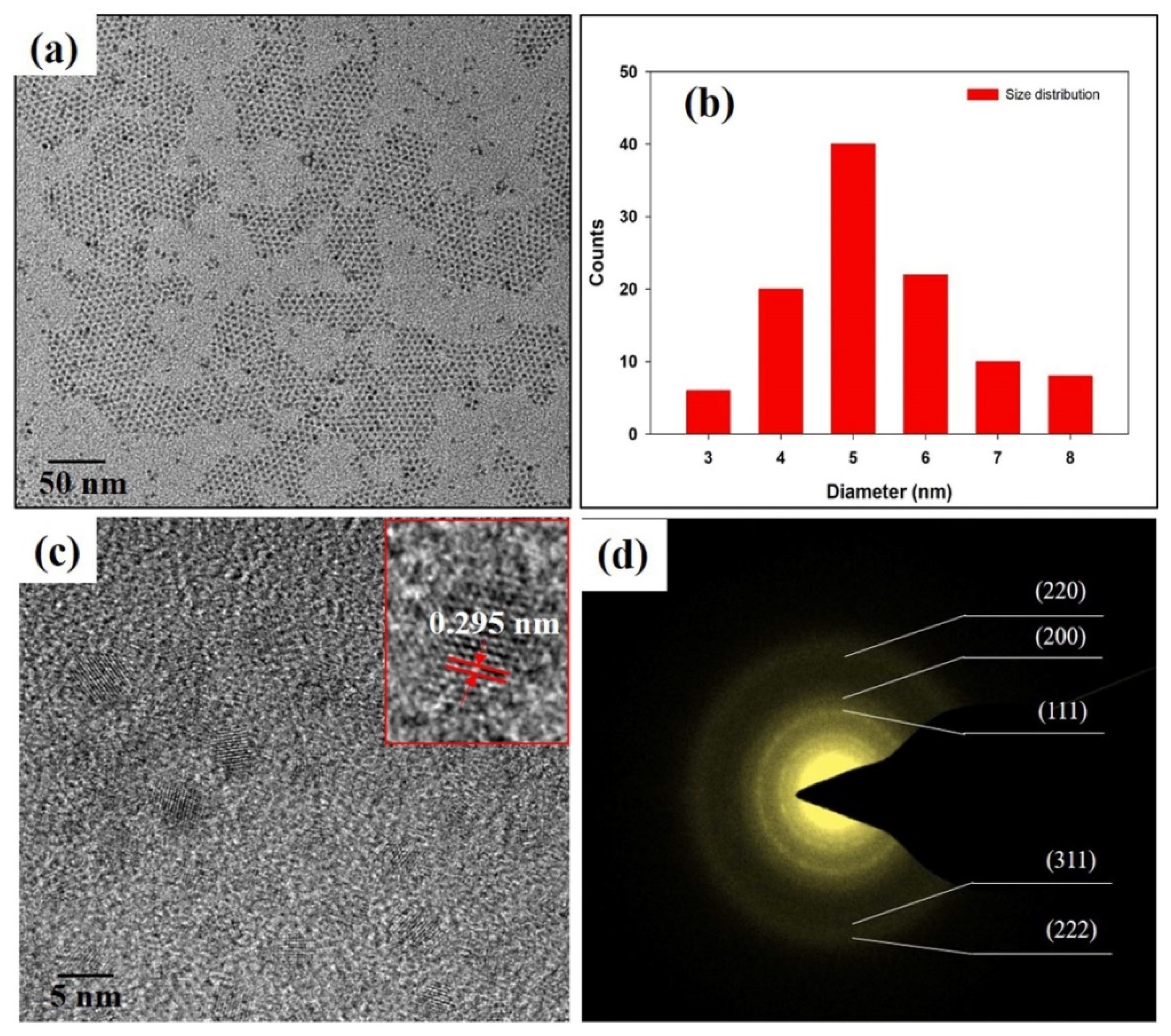
2.1. Synthesis of PbS Nanoparticles

PbS quantum dot NPs were synthesized using the modified hot-injection method [13]. In detail, 0.15 g thioacetamide was mixed with 1 mL oleylamine and 4 mL (ODE) 1-octadodecence. The mixture was stirred at ~50 °C overnight to form a sulfide (S) precursor clear solution. In a parallel step, a mixture of 0.446 g PbO, 15 mL ODE and 2 mL (OA) 1-oleic acid was stirred at 120 °C for 1 h to form a Pb precursor transparent solution. The S precursor solution was injected into the Pb precursor solution, stirred at 120 °C for 1 h and cooled down to room temperature. The product was washed four times with chloroform and dried at 70 °C to form the PbS nanoparticles.

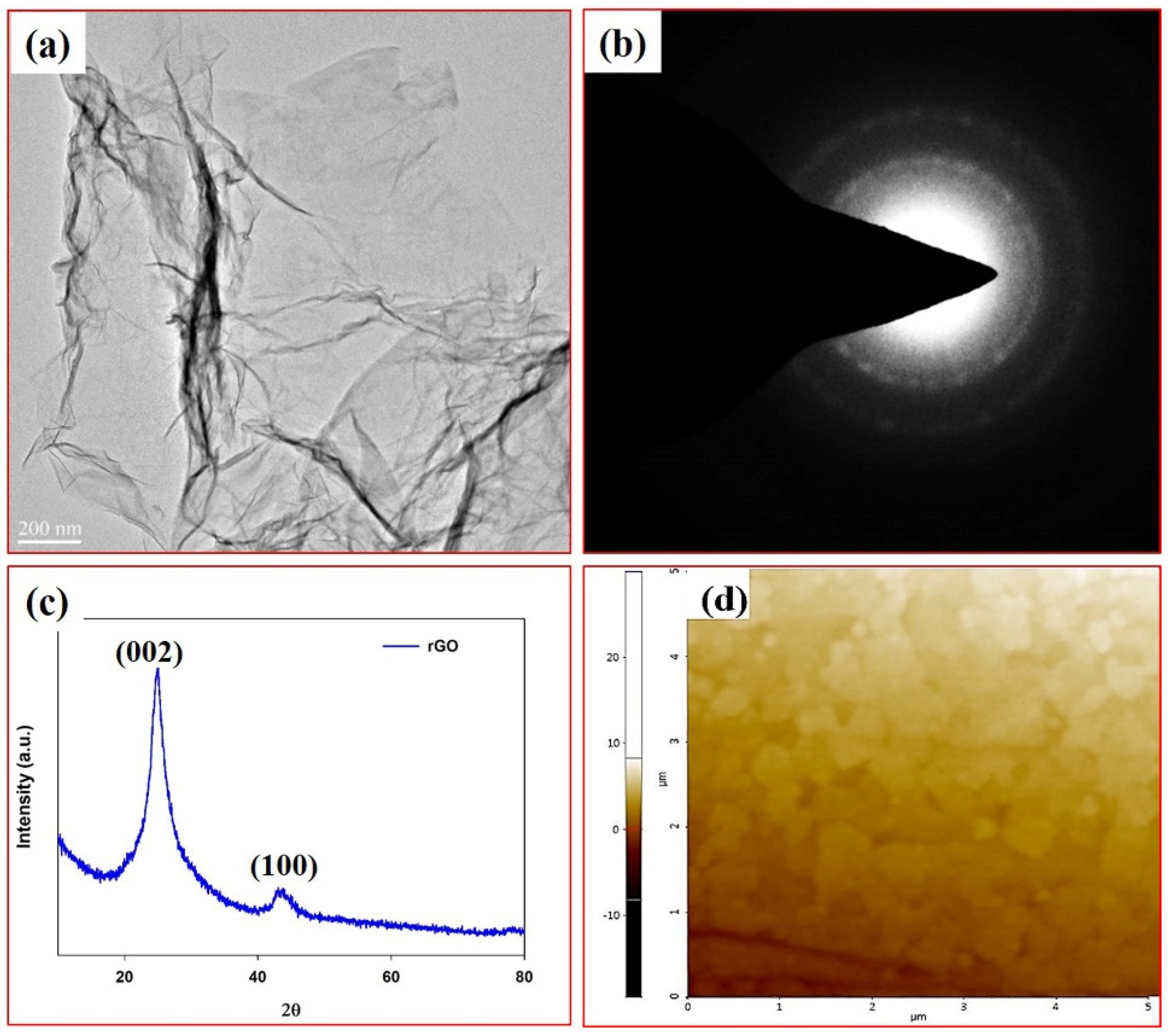
2.2. Preparation of Graphene Oxide (GO) and Reduced Graphene Oxide (rGO)

There are many modifications of the Hummers method to synthesize graphene oxide from industrially expanded graphite, which are reported elsewhere [14,15,16]. The GO sheet layer was filtered through a polycarbonate membrane filter, then dried at 90 °C for 6 h. The dried GO sheet film was processed in a Na2S2O4 solution at 70 °C for 10 min to form reduced GO. The rGO sheet layer was washed five times using deionized water and dried at 80 °C overnight in a vacuum oven.

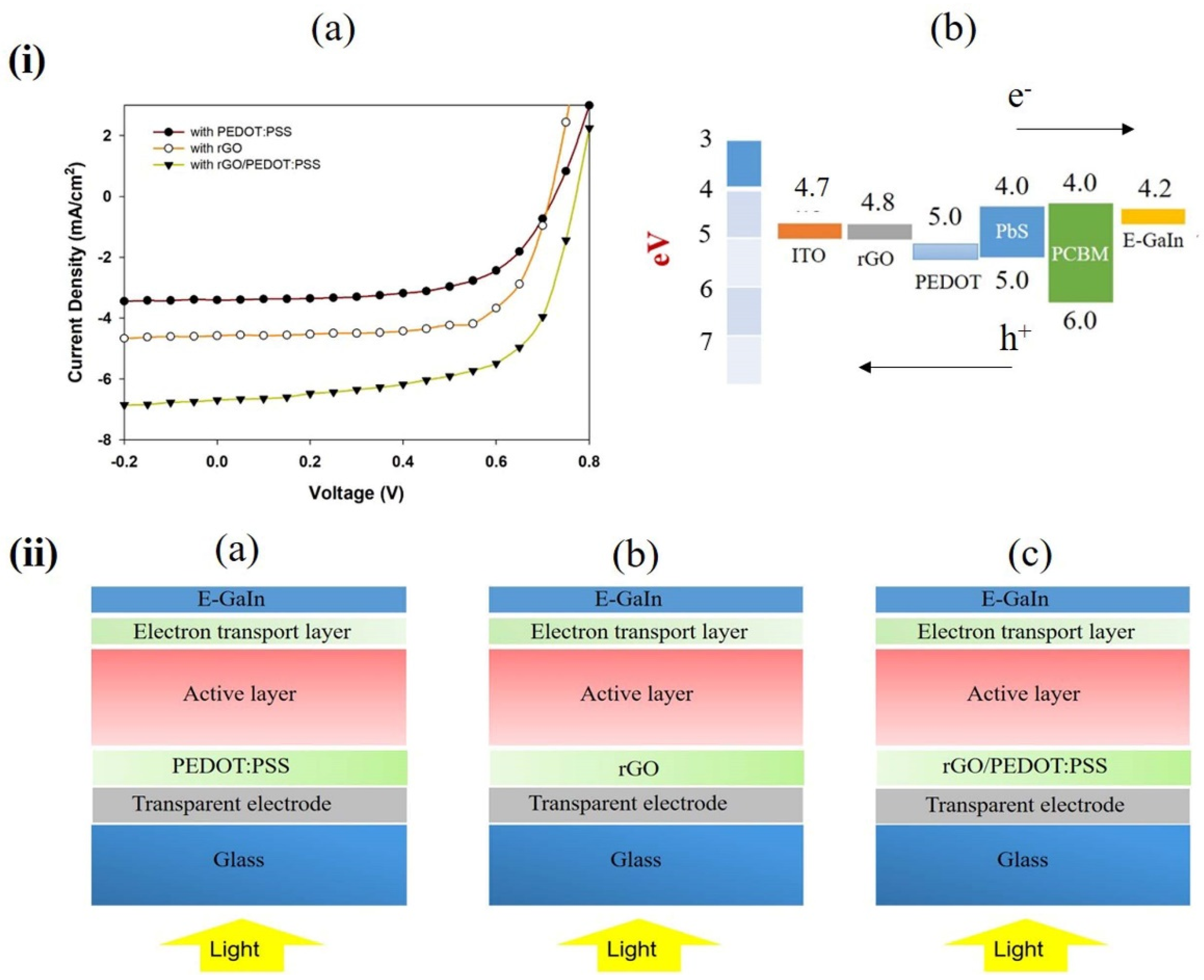
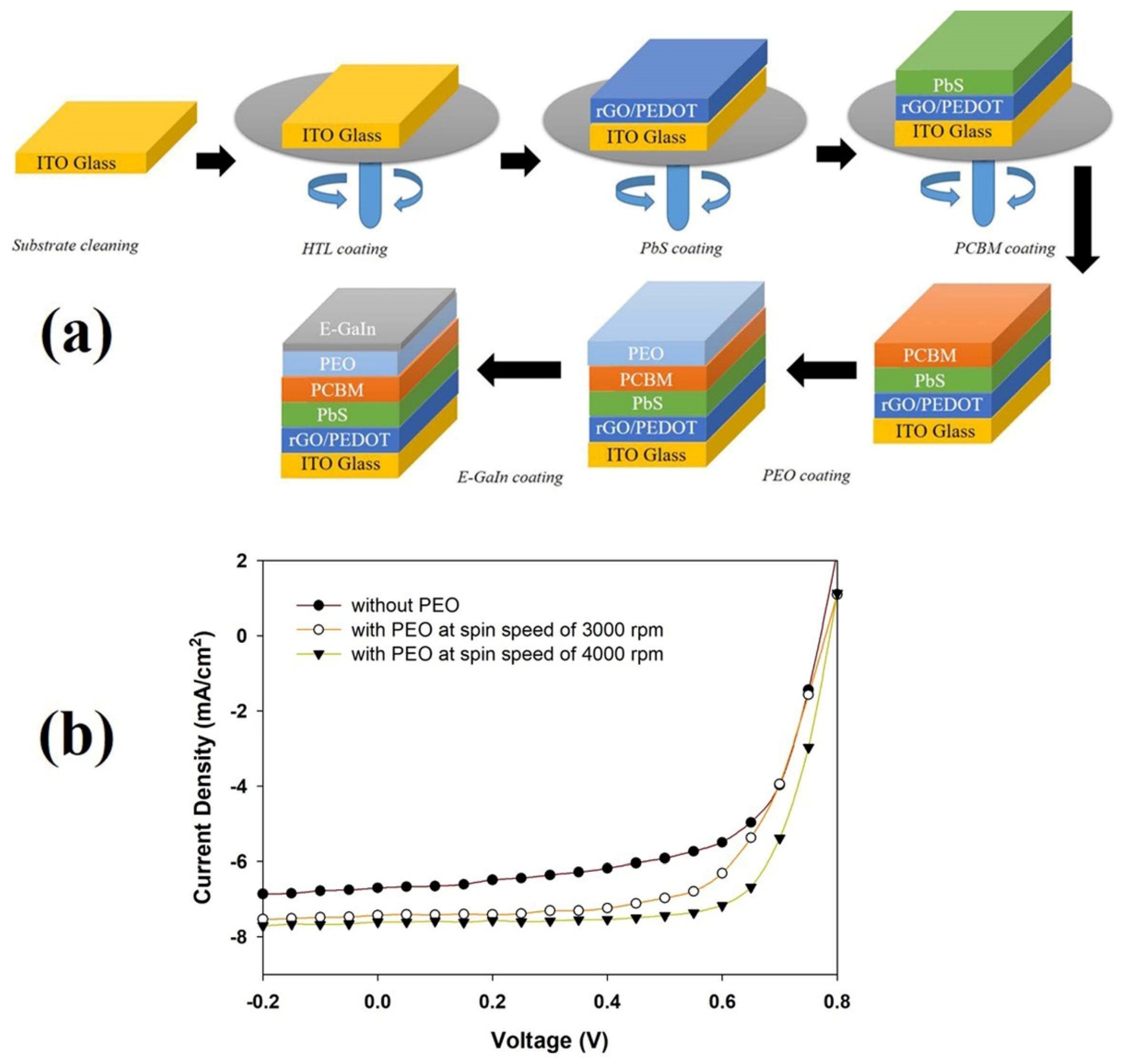
2.3. Solar Cell Fabrication

The HTLs of the rGO, PEDOT:PSS and rGO/PEDOT:PSS were coated on top of cleaned glass/ITO substrates at the speed of 4000 rpm (round per minute) for 40 s and dried at 100 °C for 30 min under nitrogen environment by using a hotplate located in the glovebox.
The PbS solution was prepared using 30 mg of PbS in 4 mL of chloroform and stirred using a hotplate at room temperature for 24 h before being coated on glass/ITO/HTL at 3000 rpm for 60s and dried at 120 °C for 30 min to form the PbS thin film. The PCBM solution was prepared using 10 mg of PCBM in 10 mL of chloroform and stirred using a hotplate at room temperature for 30 min before being coated on glass/ITO/HTL/PbS at 4000 rpm for 60 s and dried at 120 °C for 30 min to form the device active layer of glass/ITO/HTL/PbS:PCBM. Then, PEO was coated with a different spin speed for 40 s and dried at 120 °C for 30 min to form the buffer layer. Finally, E-GaIn film was deposited to complete the device’s structure of glass/ITO/HTL/(PbS:PCBM)/PEO/E-GaIn.

2.4. Characterization
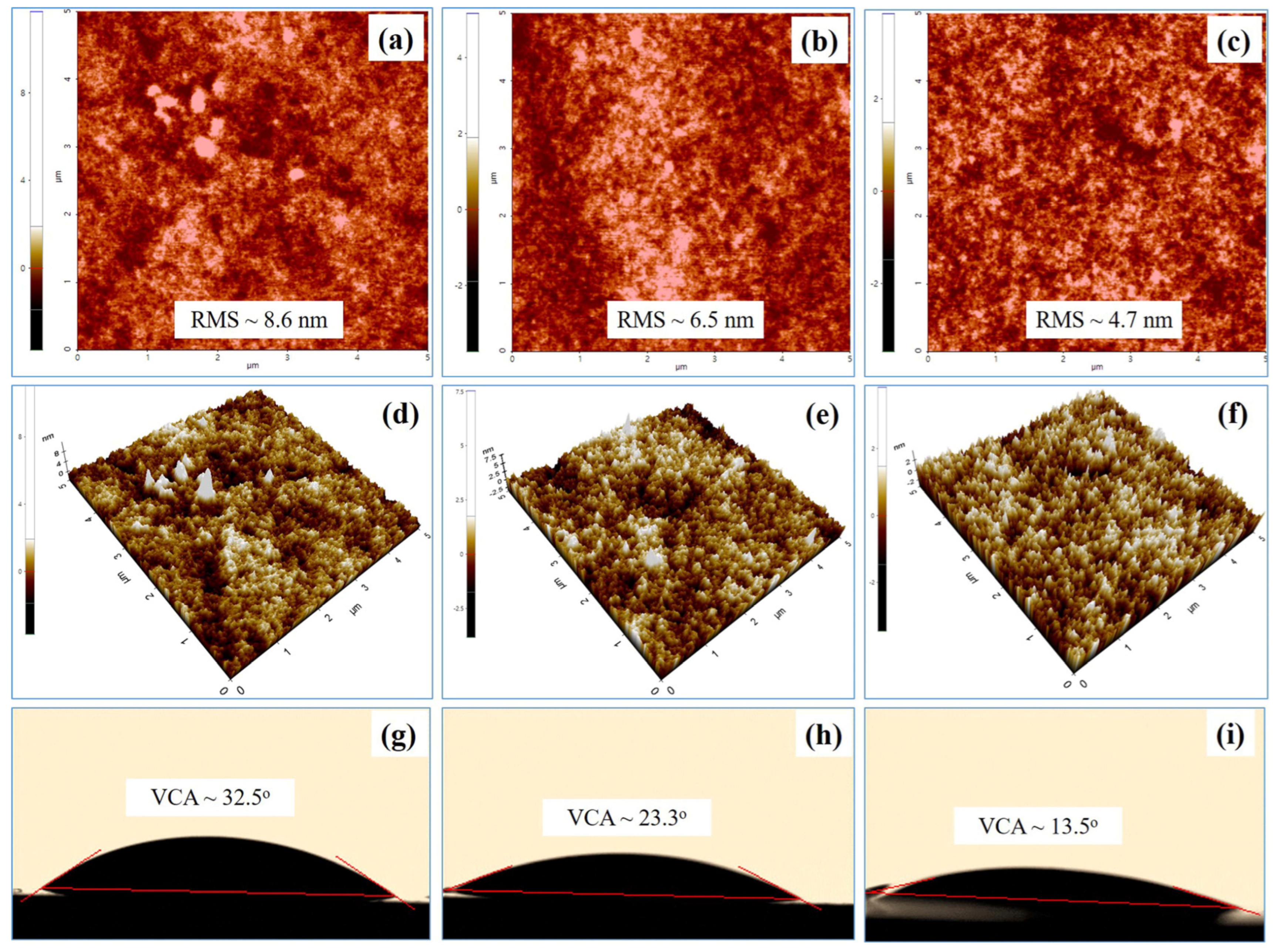
The morphological and structural properties of the PbS Qdots and rGO were measured using transmission electron microscopy (TEM), high-resolution TEM (HR-TEM) (Field Emission Transmission Electron Microscope; Model: FEI company) and X-ray diffraction (XRD) (Model: PANalytical X’ pert PRO). The topography and three-dimensionality (3D) of the surface roughness morphology (RMS) were analyzed using the atomic force microscopy (AFM) technique (Model: Park NX10). The device’s parameters, such as (FF) fill factor (%), (Jsc) short-circuit current density (mA/cm2), (Voc) open-circuit voltaic (V) and (PCE) power conversion efficiency (%) were measured using a solar simulator (Keithley 69911) (Beaverton, OR, USA) under AM 1.5 illumination at 100 mW/cm2.

3. Results

Figure 1 depicts the morphology, size and structure of the PbS QD nanocrystals, which were measured using TEM and the high-resolution TEM technique. Figure 1a shows the size of the QD in the range of 3~8 nm; it is spherical of shape and very uniform. Figure 1b is the size distribution histogram of more than 100 nanoparticles of PbS, which demonstrates that the nanoparticles are highly monodisperse and high purity, with an average diameter of 4.2 ± 0.3 nm. The high-resolution TEM image (Figure 1c—inset) of one nanoparticle reveals that the material is highly crystalline with lattice spacing of 0.295 nm. The diffraction rings in the selected-area electron diffraction pattern of the nanoparticles (Figure 1d) show the corresponding cubic rock-salt structure of bulk PbS. The pattern shows the clear planes of (111), (200), (220), (311) and (222) of PbS. This result matches well with the X-ray diffraction result in our previous work [13].
Furthermore, Figure 2a–d shows the transmission electron microscopy images of rGO. From Figure 2a, it is observed that rGO is a transparent thin sheet-layered structure, which is prepared from graphene oxide [17]. Figure 2b shows the selected area electron diffraction (SAED) pattern of the rGO, which has two rings. The outer ring is indicated by the (0001) face, whereas the inner ring is assigned to the (1100) face. The X-ray diffraction pattern of rGO is displayed in Figure 2c. There are two diffraction peaks: the first peak at the position of 2θ = 23.5° confirms that the GO was completely transformed into rGO by hydrazine solution [18] and the second peak at the position of 2θ = 43° confirms the (100) plane of the hexagonal carbon structure [19]. The surface morphology of rGO film on the glass substrates was measured using AFM technique with 5 μm × 5 μm as scan area, as shown in Figure 2d. We observed that the surface roughness of the film is ~ 3 nm.
The device performance of the VFQPH solar cells was fabricated and characterized using solar simulation under AM 1.5 illumination at 100 mW/cm2. The solar cell responses of the devices with the structure of ITO/PEDOT:PSS/PbS:PCBM/E-GaIn, ITO/rGO/PbS:PCBM/E-GaIn and ITO/rGO/PEDOT:PSS/PbS:PCBM/E-GaIn are displayed in Figure 3i,a and Table 1. The device with PEDOT:PSS as a hole transport buffer layer shows a short-circuit current, Jsc = 3.41 mA/cm2, open-circuit voltage, Voc = 0.67 V and fill factor, FF = 62%; however, the cell’s power conversion efficiency (PCE) is affected by low fill factor and current density leading to a PCE of about 1.52%. The device with rGO as a hole transport buffer layer displays a short-circuit current, Jsc = 4.58 mA/cm2, open-circuit voltage, Voc = 0.7 V, fill factor, FF = 67% and PCE of about 2.14%. The highest power conversion efficiency, PCE = 3.27%, short-circuit current, Jsc = 6.69 mA/cm2, open-circuit voltage, Voc = 0.7 V and fill factor, FF = 70% for the device with rGO/PEDOT:PSS was inserted as a hole transport buffer layer.
To study the electric contact properties in the interface between the electrode and the active layer, the material’s resistivity, such as shunt resistance (Rsh) and series resistance (Rs), should be measured to further evaluate device performance. A good solar cells device should have low series resistance and high shunt resistance. It is known that contact resistance between the active layer and electrode and the charge recombination process are affected by the values of Rs and Rsh [20,21,22,23]. Low values of shunt resistance led to the increased leakage of some current, and high values of series resistance led to decreased current density values. In the case of a solar cells device, the series resistance played a dominant role in determining the power conversion efficiency of solar cells [24,25]. A small value of Rs contributed to an increase in the charge carriers’ mobility in the photoactive layer, which led to higher efficiency.
The Rs and Rsh resistance of the devices, with and without inserting the rGO layer, were measured from the solar simulator. The highest value of series resistance, Rs = 21.3 Ωcm2, and the smallest value of current density, Jsc = 3.41 mA/cm2, led to low efficiency, PCE = 1.52%. When the rGO layer was inserted as a buffer layer, the series resistance value decreased and the value of current density increased. The lowest value of series resistance, Rs = 9.8 Ωcm2, and the highest value of current density, Jsc = 6.69 mA/cm2, of the device with rGO/PEDOT:PSS as the hole transport layer obtained the highest power conversion efficiency, PCE = 3.27%.
Figure 3i,b depicts the energy level of the device with PEDOT:PSS as an HTL and rGO as a buffer layer. Based on the literature, the work function of ITO, PEDOT:PSS and E-GaIn are ~4.7 eV, 5.0 eV and 4.2 eV, respectively [26,27,28]. The work function of rGO is 4.8 eV [29]. It was reported that the HOMO and LUMO levels of PbS are −5.0 and −4.0 eV and the HOMO and LUMO levels of PCBM are −6.0 and −4.0 eV [30]. This indicates that the reduced rGO buffer layer is capable of overcoming the energy barrier between ITO and PEDOT:PSS, which leads to improving the hole transportation from the p–n junction to the anode (ITO), resulting in the device’s efficiency increasing.
To improve the efficiency of the device, the morphology of the photoactive layer should be optimized. PEO is a good material to use as the buffer layer because PEO solubilizes well in water and many other organic solvents. Depositing PEO film without damaging the surface roughness of the active layer, and making it smoother, leads to improved device performance [31]. The PEO buffer layer with different spin-speeds (round per minute (rpm)) was inserted between the photoactive layer and back contact (E-GaIn) as an interface layer. The surface morphologies of the photoactive layer with spin-speeds of PEO were observed using atomic force microscopy (AFM) and video contact angle (VCA) techniques, as shown in Figure 4. The contact angle value is related to the film’s surface roughness and hydrophilic nature. A small contact angle value indicates that the film is highly hydrophilic and has low surface roughness.
The topography and three-dimensional (3D) images of the surface morphology of the ITO/rGO/PEDOT:PSS/PbS + PCBM without PEO layer are displayed in Figure 4a,d. The surface roughness is about ~8.6 nm and the contact angle is about 32.5°. Figure 4b,e and Figure 4c,f show the topography and 3D images of the ITO/rGO/PEDOT:PSS/PbS + PCBM with PEO of 3000 rpm (SS-3000) and 4000 rpm (SS-4000), respectively. The results show that when inserting the PEO layer between the active layer and E-GaIn layer, the surface roughness and contact angle of the device’s active layers decrease. The lowest value of roughness and contact angle are 4.7 nm and 13.5° for the sample (shown in Figure 4c,f,k, which was coated with PEO film (SS-3000)). Adding the PEO film makes the surface roughness of the active layer smoother, which leads to the improvement of the contact between the active layer and electrode. The device’s fabrication process and the complete device structure are presented in Figure 5a.
The effects of PEO buffer layer on the electrical property of the device were investigated by considering the parameters of the solar cell, as shown in Figure 5b and Table 2. The device without PEO film shows an efficiency of 3.27% (Jsc: 6.69 (mA/cm2); Voc:0.7(V); FF:70). The device with PEO (SS-3000) film has an efficiency of 3.78% (Jsc: 7.42 (mA/cm2); Voc: 0.75 (V); FF:65) and the device with PEO (SS-4000) film has an efficiency of 4.34% (Jsc: 7.61 (mA/cm2); Voc: 0.75 (V); FF:72). The device’s active layer morphology was controlled by adding PEO as a buffer layer, which led to an increase in the device’s performance. Increasing short-circuit current is related to the improvement of the contact between the electrode and the active layer. More charge carriers transported to the electrode lead to an increase in the device’s efficiency.
In this study, based on PbS quantum dots and PCBM, the parameters of vacuum-free quantum dot planar hybrid solar cells were investigated by inserting reduced rGO and PEO into the fabrication process. The device’s efficiency is still low compared with the inverted structure of quantum dot PbS solar cells and thin-film structure (PCE~10%) [32]. However, the highest current density circuit, open-circuit voltage and maximum power conversion efficiency of about 4.34% were demonstrated using a simple and vacuum-free process. This efficiency is over two times the performance of the previously reported planar hybrid PbS–organic polymer solar cells [13,30]. This value is low compared with the recorded value of the coventional invert device structure, but it can present a new structure to improve the efficiency of the quantum dot PbS solar cell, as well as the hybrid solar cells based on it.

4. Conclusions

Reduced graphene oxide and PEO were prepared and applied to VFQPH solar cells as a hole transport buffer layer and an electron transport buffer layer. The rGO/PEDOT:PSS was selected as the optimal HTBL for cell performance. The highest values of shunt resistance led to the decreased leakage of current and the lowest values of series resistance led to increased current density values. The device’s active layer surface morphology was well controlled by coats of thin PEO (SS-4000) between the active layer and the back contact E-GaIn. At the optimized structure of the glass/ITO/rGO/PEDOT:PSS/PbS:PCBM/PEO-(SS-4000)/E-GaIn device, the maximum power conversion efficiency of 4.43% (Jsc: 7.61 (mA/cm2); Voc: 0.75 (V); FF:72)) was obtained.
Our results suggest that thin layers of rGO and PEO are among the most promising candidates for the anode and cathode buffer layers in vacuum-free conventional solar cells.

Author Contributions

Writing—original draft, conceptualization, methodology and data interpretation, M.K. and N.T.N.T.; data curation, validation and resources, N.H.L. and N.L.; visualization and formal analysis, A.M.T.; writing—review and editing, M.S.T. and T.N.L.V.; supervision, project administration and funding acquisition, J.H.J. All authors have read and agreed to the published version of the manuscript.

Funding

This work was supported by the 2015 Yeungnam University Research Grant.

Institutional Review Board Statement

Not applicable.

Informed Consent Statement

Not applicable.

Data Availability Statement

Not applicable.

Conflicts of Interest

The authors declare that they have no known competing financial interests or personal relationships that could appear to influence the work reported in this paper.

References

  1. Gur, I.; Fromer, N.A.; Geier, M.L.; Alivisatos, A.P. Air-Stable All-Inorganic Nanocrystal Solar Cells Processed from Solution. Science 2005, 310, 462–465. [Google Scholar] [CrossRef] [PubMed] [Green Version]
  2. Huynh, W.U.; Dittmer, J.J.; Alivisatos, A.P. Hybrid Nanorod Polymer Solar Cells. Science 2002, 295, 2425–2427. [Google Scholar] [CrossRef] [PubMed] [Green Version]
  3. Alivisatos, A.P. Semiconductor Clusters, Nanocrystals, and Quantum Dots. Science 1996, 271, 933–937. [Google Scholar] [CrossRef] [Green Version]
  4. Luther, J.M.; Law, M.; Beard, M.C.; Song, Q.; Reese, M.O.; Ellingson, R.J.; Nozik, A.J. Schottky Solar Cells Based on Colloidal Nanocrystal Films. Nano Lett. 2008, 8, 3488–3492. [Google Scholar] [CrossRef]
  5. Barkhouse, D.A.R.; Pattantyus-Abraham, A.G.; Levina, L.; Sargent, E.H. Thiols Passivate Recombination Centers in Colloidal Quantum Dots Leading to Enhanced Photovoltaic Device Efficiency. ACS Nano 2008, 2, 2356–2362. [Google Scholar] [CrossRef]
  6. Moreels, I.; Lambert, K.; Smeets, D.; Muynck, D.; Nollet, T.; Martins, J.C.; Vanhaecke, F.; Vantomme, A.; Delerue, C.; Allan, G.; et al. Size-dependent optical properties of colloidal PbS quantum dots. ACS Nano 2009, 3, 3023–3030. [Google Scholar] [CrossRef] [Green Version]
  7. Chang, I.; Waclawik, E.R. Colloidal semiconductor nanocrystals: Controlled synthesis and surface chemistry in organic media. RCS Adv. 2014, 4, 23505–23527. [Google Scholar] [CrossRef] [Green Version]
  8. Fu, H.; Tsang, S.W. Infrared colloidal lead chalcogenide nanocrystals: Synthesis, properties, and photovoltaic applications. Nanoscale 2012, 4, 2187–2201. [Google Scholar] [CrossRef]
  9. Szendrei, K.; Gomulya, W.; Yarema, M.; Heiss, W.; Loi, M.A. PbS nanocrystal solar cells with high efficiency and fill factor. Appl. Phys. Lett. 2010, 97, 203501. [Google Scholar] [CrossRef] [Green Version]
  10. Zhai, G.M.; Bezryadina, A.; Breeze, A.J.; Zhang, D.L.; Alersand, G.B.; Carter, S.A. Air stability of TiO2/PbS colloidal nanoparticle solar cells and its impact on power efficiency. Appl. Phys. Lett. 2011, 99, 063512. [Google Scholar] [CrossRef]
  11. Choi, J.J.; Wenger, W.N.; Hoffman, R.S.; Lim, Y.F.; Luria, J.; Jasieniak, J.; Marohn, J.A.; Hanrath, T. Solution-Processed Nanocrystal Quantum Dot Tandem Solar Cells. Adv. Mater. 2011, 23, 3144–3148. [Google Scholar] [CrossRef] [PubMed]
  12. Xiea, Q.; Ming, S.; Chena, L.; Wub, Y.; Zhangb, W.; Liu, X.; Cao, M.; Wang, H.Q.; Fang, J. Parameters in planar quantum dot-polymer solar cell: Tuned by QD Eg, ligand exchange and fabrication process. Org. Electron. 2019, 69, 1–6. [Google Scholar] [CrossRef]
  13. Trinh, T.K.; Truong, N.T.N.; Pham, V.T.H.; Park, C. Simple and Green Synthesis of Lead Sulfide Nanocrystals for Hybrid Bulk Hetero-Junction Solar Cells. Sci. Adv. Mater. 2016, 8, 601–606. [Google Scholar] [CrossRef]
  14. Hummers, W.S.; Offeman, R.E. Preparation of graphitic oxide. J. Am. Chem. Soc. 1958, 80, 1339. [Google Scholar] [CrossRef]
  15. Ryu, M.S.; Jang, J. Effect of solution processed graphene oxide/nickel oxide bilayer on cell performance of bulk-heterojunction organic photovoltaic. Sol. Energy Mater. Sol. Cells 2011, 95, 2893–2896. [Google Scholar] [CrossRef]
  16. Chen, D.; Li, L.; Guo, L. An environmental-friendly preparation of reduced graphene oxide nanosheets via amino acid. Nanotechnology 2011, 22, 32567–325601. [Google Scholar] [CrossRef]
  17. Liu, H.; Li, P.; Bai, H.; Du, C.; Wei, D.; Su, Y.; Wang, Y.; Yang, L. Incorporation of reduced graphene oxide into faceted flower-like {001} TiO2 for enhanced photocatalytic activity. R. Soc. Open Sci. 2018, 5, 180613. [Google Scholar] [CrossRef] [Green Version]
  18. Khenfouch, M.; Buttner, U.; Baitoul, M.; Maaza, M. Synthesis and characterization of mass produced high quality few layered graphene sheets via a chemical method. Graphene 2014, 3, 7–13. [Google Scholar] [CrossRef] [Green Version]
  19. Zhan, Y.; Meng, F.; Lei, Y.; Zhao, R.; Zhong, J.; Liu, X. Solid state NMR of immobilized catalysts and nanocatalysts. Mater. Lett. 2011, 65, 1737–1740. [Google Scholar] [CrossRef]
  20. Chen, T.L.; Chen, J.J.A.; Catane, L.; Ma, B. Fully solution processed pin organic solar cells with an industrial pigment—Quinacridone. Org. Electron. 2011, 12, 1126–1131. [Google Scholar] [CrossRef]
  21. Wang, K.; Zheng, Y.; Xu, G.; Xu, X. The inverse correlation between series resistance and parallel resistance of small molecule organic solar cells. Prog. Nat. Sci. 2015, 25, 323–326. [Google Scholar] [CrossRef] [Green Version]
  22. Rusu, M.; Wiesner, S.; Lauermann, I.; Fischer, C.H.; Fostiropoulos, K.; Audinot, J.N.; Fleming, Y.; Steiner, M.C.L. Formation of charge-selective Mg–Ag electrodes to CuPc:C60 blend layers. Appl. Phys. Lett. 2010, 97, 073504. [Google Scholar] [CrossRef]
  23. Lloyd, M.T.; Mayer, A.C.; Tayi, A.S.; Bowen, A.M.; Kasen, T.G.; Herman, D.J.; Mourey, D.A.; Anthony, J.E.; Malliaras, G.G. Photovoltaic cells from a soluble pentacene derivative. Org. Electron. 2006, 7, 243–248. [Google Scholar] [CrossRef]
  24. Colinge, J.P.; Colinge, C.A. Physics of Semiconductor Devices, 3rd ed.; Kluwer Academic Publishers: New York, NY, USA, 2007; pp. 77–133. [Google Scholar]
  25. Servaites, J.D.; Yeganeh, S.; Marks, T.J.; Ratner, M.A. Efficiency enhancement in organic photovoltaic cells: Consequences of optimizing series resistance. Adv. Funct. Mater. 2010, 20, 97–104. [Google Scholar] [CrossRef]
  26. Park, Y.; Choong, V.; Gao, Y.; Hsieh, B.R.; Tang, C.W. Work function of indium tin oxide transparent conductor meas-ured by photoelectron spectroscopy. Appl. Phys. Lett. 1996, 68, 2699–2701. [Google Scholar] [CrossRef]
  27. Mengistie, D.A.; Ibrahem, M.A.; Wang, P.C.; Chu, C.W. Highly Conductive PEDOT:PSS Treated with Formic Acid for ITO-Free Polymer Solar Cells. ACS Appl. Mater. Interfaces 2014, 6, 2290–2297. [Google Scholar] [CrossRef]
  28. Chiechi, R.C.; Weiss, E.A.; Dickey, M.D.; Whitesides, G.M. Eutectic Gallium–Indium (EGaIn): A Mold-able Liquid Metal for Electrical Characterization of Self-Assembled Monolayers. Angew. Chem. Int. Ed. 2008, 47, 142–144. [Google Scholar] [CrossRef]
  29. Schmiedova, V.; Pospisil, J.; Kovalenko, A.; Ashcheulov, P.; Fekete, L.; Cubon, T.; Peter, K.; Oldrich, Z.; Weiter, M. Physical properties investigation of reduced graphene oxide thin films prepared by material inkjet printing. J. Nanomater. 2017, 2017, 1–8. [Google Scholar] [CrossRef] [Green Version]
  30. Zhao, N.; Osedach, T.P.; Chang, L.Y.; Geyer, S.M.; Wanger, D.; Binda, M.T.; Alexi, C.A.; Moungi, G.B.; Bulovic, V. Colloidal PbS quantum dot solar cells with high fill factor. ACS Nano 2010, 4, 3743–3752. [Google Scholar] [CrossRef]
  31. Kim, H.P.; Yusoff, A.R.; Jang, J. Organic solar cells using a reduced graphene oxide anode buffer layer. Sol. Energy Mater. Sol. Cells 2013, 110, 87–93. [Google Scholar] [CrossRef]
  32. Bordi, F.; Cametti, C.; Di Biasio, A. Electrical conductivity behavior of poly (ethylene oxide) in aqueous electrolyte solutions. Am. J. Phys. Chem. 1988, 92, 4772–4777. [Google Scholar] [CrossRef]
Figure 1. (a) Transmission electron microscopy (TEM) image of PbS nanoparticles, (b) size histogram of PbS nanoparticles, (c) high-resolution TEM image a PbS nanocrystal and (d) selected area electron diffraction pattern of PbS nanocrystal.
Applsci 12 01185 g001
Figure 2. (a) Transmission electron microscopy (TEM) image of rGO, (b) selected area electron diffraction pattern of rGO, (c) X-ray diffraction pattern of rGO and (d) surface morphology of rGO film on the glass substrate.
Applsci 12 01185 g002
Figure 3. (i) (a) Current density-voltage curve of photovoltaic devices based on different hole transport layers and (b) the energy level alignment of devices with PEDOT:PSS as the HTL and rGO as the buffer layer. (ii) Device structure (a) ITO/PEDOT:PSS/PbS:PCBM/E-GaIn, (b) ITO/rGO/PbS:PCBM/E-GaIn, (c) ITO/rGO/PEDOT:PSS/PbS:PCBM/E-GaIn.
Applsci 12 01185 g003
Figure 4. (ac) Topography and (df) 3D AFM images of ITO/rGO/PEDOT:PSS/PbS:PCBM layer without and with the PEO buffer layer; (gk) video contact angle images.
Applsci 12 01185 g004
Figure 5. (a) Device fabrication process and (b) the current density-voltage (J-V) curves of the device without and with the PEO buffer layer.
Applsci 12 01185 g005
Table 1. Device parameters as open-circuit voltage (Voc), short-circuit current density (Jsc), fill factor (FF) and power conversion efficiency (PCE) from J-V characteristics for different hole transport layers; with PEDOT:PSS, rGO and rGO/PEDOT:PSS under A.M 1.5G illumination at 100 mW/cm2.
Device StructureJsc
(mA/cm2)
Voc
(V)
FF
(%)
Eff
(%)
With PEDOT:PSS3.41 ± 0.020.67 ± 0.0362 ± 41.52 ± 0.02
With rGO4.58 ± 0.010.70 ± 0.0267 ± 22.14 ± 0.01
With rGO/PEDOT:PSS6.69 ± 0.010.70 ± 0.0070 ± 23.27 ± 0.01
Table 2. Device parameters as open-circuit voltage (Voc), short-circuit current density (Jsc), fill factor (FF) and power conversion efficiency (PCE) from J-V characteristics without and with different PEO buffer layer thickness under A.M 1.5G illumination at 100 mW/cm2.
Device StructureJsc
(mA/cm2)
Voc
(V)
FF
(%)
Eff
(%)
Without PEO6.69 ± 0.010.70 ± 0.0070 ± 23.27 ± 0.01
With PEO (SS-3000 rpm)7.42 ± 0.020.75 ± 0.0265 ± 23.78 ± 0.02
With PEO (SS-4000 rpm)7.61 ± 0.020.75 ± 0.0072 ± 24.34 ± 0.01
Publisher’s Note: MDPI stays neutral with regard to jurisdictional claims in published maps and institutional affiliations.

